Off
Add to Calendar2025-12-02 00:00:002025-12-02 00:00:002025 Semiconductor Innovation and Intelligent Application Summit (SIIAS)New Territories Hong Kong ChinaSEMI.org[email protected]America/Los_Angelespublic
Smart Sensors and Edge Intelligence for Advanced Process Control
Overview: Explore the latest sensor technologies—optical, thermal, vibration, and chemical—and how embedded AI at the edge enables real-time control loops for critical wafer fab processes. Includes case studies on inline metrology and adaptive control.
Key Topics: Sensor fusion and calibration, Edge inference for process drift detection, Integration with APC and FDC system
Smart Sensors and Edge Intelligence for Advanced Process Control
Overview: Explore the latest sensor technologies—optical, thermal, vibration, and chemical—and how embedded AI at the edge enables real-time control loops for critical wafer fab processes. Includes case studies on inline metrology and adaptive control.
Key Topics: Sensor fusion and calibration, Edge inference for process drift detection, Integration with APC and FDC system
8:00 am
-
8:45 am
Registration & Breakfast
8:45 am
-
8:55 am
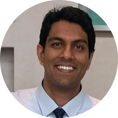
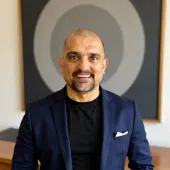
Anshu Bahadur
SEMI
Day 1 - Welcome All
Welcome & SEMI Manufacturing Coalitions Overview
8:55 am
-
9:30 am
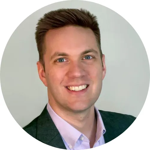
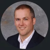
Russell Dover
General Manager, Service Product Line
LAM
Keynote: Vision – Edge Inference – Process Control, APC, FDC
9:30 am
-
9:55 am
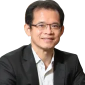
James Bramante
Senior Data Scientist
INFICON
Managing Edge AI for Smart Sensor Process Control
9:55 am
-
10:20 am
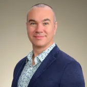
Robert Hillinger
Industry Leader Semiconductor
Kistler
Advanced Process Control with Piezoelectric Sensor Fusion for Semiconductor Manufacturing
10:20 am
-
10:35 am
Coffee Break
10:35 am
-
11:00 am
Chris Dickens
Application Eng
Beckhoff Automation
A Unified Industrial Platform for Production-Ready AI
11:00 am
-
11:25 am
Gokul Sathya
Research Scientist
Siemens
Physical AI on the Manufacturing Floor: From Virtual Commissioning to Deployment
11:25 am
-
11:50 am
Aumkar Renavikar
Chief Product Officer, Co-Founder & CTO
Parallax Worlds
Intelligent Robots & Digital Twins for Advanced Manufacturing
11:50 am
-
12:05 pm
Chakravarthy Elumalai
CTO
Ray Vector
Sensor as the Eyes and Ears of AI
12:05 pm
-
1:00 pm
Networking Lunch
Afternoon, Day 1: March 18th, 2026
.
Yield Enhancement through Edge-Driven Defect Detection and Classification
Overview: Present how edge AI models process sensor and image data to identify yield-impacting defects early in the process. Discuss virtual metrology, anomaly detection, and feedback loops for yield optimization.
Key Topics: Real-time defect classification, Sensor-based yield prediction, Integration with SPC and yield dashboards
1:00 pm
-
1:05 pm
Karim Somani
SEMI
SEMI Fab Owners Alliance (FOA)
1:05 pm
-
1:35 pm
Surya Kalidindi
Co-Founder
Multiscale
Physics-Aware AI for Semiconductor Manufacturing Process Optimization: Deployed Systems and the Edge AI Frontier
1:35 pm
-
2:00 pm
Maryia Kurdina
AI R&D Group Leader, Technology & AI Design Research Center
TEL
Real-Time, Tool-Independent Health Monitoring Using Gaussian Process Confidence Bands on Sensor Signals
2:00 pm
-
2:25 pm
Avni Agarwal
Co-Founders & CTO
SixSense
Applications of AI-Based Defect Classification for Yield Improvement: From FEOL (Front end-of line) in Fabs to Assembly and Test
2:25 pm
-
2:40 pm
Coffee Break
2:40 pm
-
3:05 pm
Arjun Hegde
Senior Application Engineering Manager
KLA
Edge-Driven Yield Learning: Real-Time Deep Learning and HAR Defect Discovery in Advanced E-Beam Architectures
3:05 pm
-
3:30 pm
Prasad Bachiraju
Senior Director, Business Development
Onto Innovation
Reducing Rework and Boosting Fab Capacity with Edge AI and Metrology-Driven Predictive Analytics
3:30 pm
-
3:55 pm
Danny Krastev
Full Stack AI Developer
Microtronic
Overcoming the challenges of AI defect detection and classification of semiconductor macro defects
3:55 pm
-
4:20 pm
Chengli He
Industry Manager
MathWorks
From Data to Decisions: Edge AI for Yield, Defect Detection, and Predictive Insights
4:20 pm
-
4:35 pm
Stephen March
Semiconductor Leader
Schneider
Software Defined Industrial Automation: A Blueprint for AI-Ready, Real-Time Edge Operations in Semiconductor Manufacturing
4:35 pm
-
6:35 pm
Reception
Morning, Day 2: March 19th, 2026
Autonomous WIP Movement: Robots, Sensors, and Edge AI Coordination
Overview: Dive into next-gen clean rooms – how intelligent robotics & AI‑enabled inspection elevate yield, reliability & efficiency.
Key Topics: Sensor-guided AGVs and AMRs, AI-based path optimization, Interoperability with fab logistics systems
8:00 am
-
8:45 am
Registration & Breakfast
8:45 am
-
8:55 am
Paul Carey and Melissa Grupen-Shemansky
SEMI
Day 2 - Welcome All
Day 1 Overview & MSIG Overview
8:55 am
-
9:30 am
Carlos O’Farrill
Global Key Account Manager
KUKA
Keynote: Smarter Fabs in Motion: How Edge AI and Sensor Networks Drive Autonomous Material Handling
9:30 am
-
9:55 am
Vidya Vijay
Director, Business Development, Growth & Strategy
Nordson
Precision, Automation, and Beyond: The Role of Advanced Sensors in the Evolution of Semiconductor Manufacturing for effective Tool set-up, Predictive and Preventative Maintenance
9:55 am
-
10:20 am
Joseph Tsao
US Sales Director
Solomon 3-D
Perception-Enabled Assurance of Semiconductor Manufacturing Systems
10:20 am
-
10:35 am
Coffee Break
10:35 am
-
11:00 am
Murali Krishna
Vice President of Products
Minds.ai
Using Edge AI models and Deep RL to improve yield, tool availability, and fab performance
11:00 am
-
11:25 am
Michael Bowcutt
Director of Sales Engineering
CamLine
Solving the Interoperability Gap: Orchestrating and Emulating Mixed-Fleet Robotics for High-Yield Fabs
11:25 am
-
11:50 am
Greg Berger
Solution Consultant
Rockwell Automation
Smart Modular Conveyance, the first step towards Autonomous Operations in Analog & Legacy fabs
11:50 am
-
12:15 pm
Brian Zmikly
Sr. Director, US Enterprise & Government Sales, 5G Acceleration
Verizon
The 5G Fabric: Leveraging Next Gen Connectivity to Enable Automation and Intelligence
12:15 pm
-
12:30 pm
Anshu Bahadur
SEMI
Robots in the Cleanroom: Future of Automation in Semiconductor Manufacturing
12:30 pm
-
1:30 pm
Networking Lunch
Afternoon, Day 2: March 19th, 2026
Predictive Maintenance at the Edge: From Vibration to Vision
Overview: Highlight how edge-deployed AI models use sensor data (vibration, acoustic, thermal, visual) to predict equipment failures before they occur. Showcase deployment strategies and ROI from reduced downtime.
Key Topics: Edge analytics for tool health, Federated learning across equipment fleets, Maintenance scheduling optimization
1:30 pm
-
2:05 pm
James Bramante
Senior Data Scientist
INFICON
Keynote: Predictive Maintenance at the Edge - AI Enabling PdM
2:05 pm
-
2:30 pm
Michael Passow
AI Semiconductor Factory Automation Program Manager
IBM
Edge AI–Enabled Predictive Maintenance: Closing the Loop Between Equipment Health and Fab Operations
2:30 pm
-
2:55 pm
Mauro Riboni
Technical lead – Alliance & Partnership
Bosch
The Edge Revolution: Predictive Maintenance Reborn with Edge AI
2:55 pm
-
3:20 pm
Paul Johnson
Senior Manager – Digital Transformation
Edwards
The Challenge Of AI At The Edge – Making Use Of Advanced Sensors
3:20 pm
-
3:35 pm
Coffee Break
3:35 pm
-
4:00 pm
Sainyam Galhotra
Co-founder & Faculty, Cornell University
Third AI Automation
Edge-based Defect Detection and Predictive Maintenance in Semiconductor Manufacturing
4:00 pm
-
4:25 pm
Sundeep Ahluwalia
Chief Product Officer
TDK SensEI
Edge AI: The Future of Industrial Machine Health Monitoring
4:25 pm
-
4:50 pm
Kelli Case
Business Development Director, Senseye Predictive Maintenance
Siemens
How AI‑based Maintenance Can Reshape Semiconductor Operations By Cutting Downtime By Up To 50%
Unlocking Smarter, More Autonomous Fabs with Edge AI
As semiconductor fabs strive for higher yield, uptime, and efficiency, AI at the edge is becoming central to semiconductor manufacturing. Modern edge devices combine advanced sensors with embedded AI to monitor equipment, optimize energy, and detect anomalies in real time - without relying on the cloud.
This workshop will explore how AI-driven sensors and edge intelligence, integrated with IoT, 5G, and AI accelerators, enable scalable, resilient, and intelligent solutions tailored for semiconductor manufacturing. Learn how these technologies support:
Predictive maintenance to prevent downtime
Adaptive process automation for maximum efficiency
Real-time decision-making at the source of data generation
Join us to see how the convergence of sensors, edge AI, and connectivity is unlocking the next era of smart manufacturing.
Smarter Sensors, Smarter Fabs: AI at the Edge in Semiconductor Manufacturing
In-Person Workshop | March 18-19, 2026 | Milpitas, CA
Off
Add to Calendar2026-03-18 00:00:002026-03-19 00:00:00Smarter Sensors, Smarter Fabs: AI at the Edge in Semiconductor ManufacturingUnlocking Smarter, More Autonomous Fabs with Edge AIAs semiconductor fabs strive for higher yield, uptime, and efficiency, AI at the edge is becoming central to semiconductor manufacturing. Modern edge devices combine advanced sensors with embedded AI to monitor equipment, optimize energy, and detect anomalies in real time - without relying on the cloud.This workshop will explore how AI-driven sensors and edge intelligence, integrated with IoT, 5G, and AI accelerators, enable scalable, resilient, and intelligent solutions tailored for semiconductor manufacturing. Learn how these technologies support:Predictive maintenance to prevent downtimeAdaptive process automation for maximum efficiencyReal-time decision-making at the source of data generationJoin us to see how the convergence of sensors, edge AI, and connectivity is unlocking the next era of smart manufacturing.Milpitas, CA United StatesSEMI.org[email protected]America/Los_Angelespublic
America/Los_Angeles
On Demand
A digital twin is a computer representation of the structure, context, and behavior of physical systems, which are critical components in the optimization of computational systems, accurately representing physical systems and processes. A Digital Twin can be used to reduce or eliminate iterative physical experiments needed for optimization, thereby enhancing yield, saving time, and resources. Semiconductor manufacturing involves numerous complex steps, where accurate control of each step is crucial to achieving the overall manufacturing yield and minimizing variations in device characteristics. The complexity of the manufacturing processes' flows limits flexibility for testing novel approaches. Unit processes can be based on first-principal models (physics-based), data-based models, or hybrid models combining both approaches when possible. Fabrication processes in the cleanroom and on printed electronics tools are often a function of time-varying parameters, including those of the equipment, environment, and materials. The parameters often have co-dependencies across different process steps and tool sets.
This course will cover the necessary material to create DNN-based Digital twins for nanofabrication processes in cleanrooms. The course will include experimental details for data preparation, data processing, training models, and use case demonstrations. Nanofabrication process equipment can inherently have millions of internal variables and can learn from datasets, providing a robust and complementary approach to traditional feedback control and process stabilization methods. The included Digital Twin modes are developed using images (CD-SEMs, optical images), time history data (Optical Emission Spectroscopy), and textual process information (recipes and materials). The course will include: (1) Approaches to preprocess image data and create learning-based models, (2) using DNN-based domain translation for learning to predict the DUV nanolithography and ICP Plasma Etch, (3) virtual metrology methods for quantification of learning outcomes, and (4) developing a new class of process-aware DNN-based digital twins.
ABOUT THE SPEAKERS
Benyamin Davaji, PhD Benyamin Davaji is an Assistant Professor in the Electrical and Computer Engineering Department at Northeastern University. His research focuses on integrated microsystems with an emphasis on sensing and computation using mechanical waves, acoustic/ultrasound transducers, bio-interfaces, and microcalorimetry. He also applies data-guided methods to nanofabrication process development and semiconductor manufacturing. Dr. Davaji earned his PhD in Electrical and Computer Engineering from Marquette University in 2016 and later served as a post-doctoral associate at Cornell University’s School of Electrical and Computer Engineering.
Peter Doerschuk, PhD
Peter Doerschuk, Professor at Cornell University since 2006, previously served on the Purdue faculty in Electrical and Computer Engineering and Biomedical Engineering. He earned B.S., M.S., and Ph.D. degrees in Electrical Engineering from MIT, an M.D. from Harvard Medical School, and completed training at Brigham and Women’s Hospital and a postdoc at MIT. His research applies computational nonlinear stochastic systems to biology and medicine, spanning viral 3-D structure determination using electron microscopy and x-ray scattering, to nonlinear models of ethanol pharmacokinetics that enable sensor processing, pattern recognition, and individualized physiological analysis.
Join us for this engaging Master Class with Benyamin Davaji, PhD, Assistant Professor of Electrical and Computer Engineering at Northeastern University and Peter Doerschuk, Professor of Electrical and Computer Engineering and Biomedical Engineering at Cornell University, as they explore the role of digital twin models in advancing semiconductor manufacturing. The masterclass will highlight how data-guided methods and computational modeling are transforming unit process development, driving efficiency and innovation across the semiconductor industry. With expertise spanning microsystems, acoustic transducers, and nanofabrication, the speakers will provide insights into how digital twins can bridge research and production to accelerate breakthroughs in semiconductor technology.
Digital Twin Models for Semiconductor Manufacturing Unit Process
Flexible Electronics Master Class #27
10:00 am - 12:00 pm
Off
Add to Calendar2025-11-05 10:00:002025-11-05 12:00:00FEMC#27 Digital Twin Models for Semiconductor Manufacturing Unit ProcessJoin us for this engaging Master Class with Benyamin Davaji, PhD, Assistant Professor of Electrical and Computer Engineering at Northeastern University and Peter Doerschuk, Professor of Electrical and Computer Engineering and Biomedical Engineering at Cornell University, as they explore the role of digital twin models in advancing semiconductor manufacturing. The masterclass will highlight how data-guided methods and computational modeling are transforming unit process development, driving efficiency and innovation across the semiconductor industry. With expertise spanning microsystems, acoustic transducers, and nanofabrication, the speakers will provide insights into how digital twins can bridge research and production to accelerate breakthroughs in semiconductor technology.United StatesSEMI.org[email protected]America/Los_Angelespublic
America/Los_Angeles
Watch On-Demand
Sponsoring will associate your company with the industry's most respected senior executives. Sponsorship opportunities can be tailored to meet your specific branding and marketing objectives.
The Surface Preparation and Cleaning Conference (SPCC) is a premier technical forum dedicated to advancing surface preparation, cleaning technologies, and wet processes essential to semiconductor manufacturing. Formerly presented by Linx Consulting, SPCC continues its legacy of delivering high-quality technical content through invited presentations, peer-reviewed sessions, and poster presentations covering all aspects of cleaning science, process integration, materials, equipment, and metrology.
SPCC will feature invited business-focused presentations that examine macroeconomic, market, and structural trends shaping the global semiconductor industry that were formerly included in the Business Interface Conference (BIC). These sessions will provide attendees with valuable context on industry dynamics, supply chain, and strategic outlooks that complement the technical discussions at SPCC.
Now a unified conference, SPCC unites both business and technical aspects of industry into a comprehensive program that bridges technology development and business strategy, offering attendees enhanced opportunities for cross-disciplinary learning, collaboration, and networking with industry leaders, researchers, and decision-makers across the semiconductor ecosystem.
Join our premier technical forum with topics including—
Cleaning Science
Equipment
Industry Dynamics
Materials
Metrology
Process Integration
Strategic Outlook
Supply Chain
Wild Horse Pass 5040 Wild Horse Pass Blvd Chandler, AZ , AZ85226 United States
Surface Preparation and Cleaning Conference (SPCC), formerly presented by Linx Consulting, brings together key business insights, IC manufacturers, equipment makers, materials and chemical providers, metrology experts, process technologists to address critical challenges, and innovations in surface preparation and cleaning.
Held at the Wild Horse Pass Resort in Chandler, Arizona, SPCC 2026 will feature technical sessions, poster presentations, and business-focused programming, creating a unique forum where technology and industry strategy converge.
Surface Preparation & Cleaning Conference—SPCC
May 18–20, 2026
Wild Horse Pass, Chandler, AZ
Off
Add to Calendar2026-05-18 00:00:002026-05-20 00:00:00SPCC 2026—Surface Preparation & Cleaning Conference Surface Preparation and Cleaning Conference (SPCC), formerly presented by Linx Consulting, brings together key business insights, IC manufacturers, equipment makers, materials and chemical providers, metrology experts, process technologists to address critical challenges, and innovations in surface preparation and cleaning.Held at the Wild Horse Pass Resort in Chandler, Arizona, SPCC 2026 will feature technical sessions, poster presentations, and business-focused programming, creating a unique forum where technology and industry strategy converge.Wild Horse Pass 5040 Wild Horse Pass Blvd Chandler, AZ , AZ 85226 United StatesSEMI.org[email protected]America/Phoenixpublic
America/Phoenix
Join us for an insightful webinar as we present the findings from the 2025 Semiconductor Supply Chain Survey, a collaborative effort between the SEMI Supply Chain Management initiative and McKinsey & Company.
The annual survey aims to establish benchmarks for operational agility metrics, covering the entire value chain from material suppliers to OEMs, offering a comprehensive view of the landscape. New this year are additional insights on trends in LTAs and organizational supply chain management capabilities
During this webinar, we will share results from the survey uncovering key trends, challenges, and opportunities within the semiconductor supply chain. By attending, you'll gain valuable insights to benchmark your organization against peers, identify areas for improvement, and course-correct more effectively. Please contact us if you like to learn about how your company can participate in the SCM initiative.
Join us for a webinar highlighting the 2025 Semiconductor Supply Chain Survey results, conducted by SEMI SCM initiative and McKinsey & Company. Gain fresh insights into operational agility, LTAs, and SCM capabilities across the value chain. Discover key trends, challenges, and opportunities to benchmark your organization and strengthen supply chain resilience.
2025 Semiconductor Supply Chain survey: Insights for strategy and capabilities
9:00 am - 10:00 am
Off
Add to Calendar2025-09-23 09:00:002025-09-23 10:00:002025 Semiconductor Supply Chain survey: Insights for strategy and capabilitiesJoin us for a webinar highlighting the 2025 Semiconductor Supply Chain Survey results, conducted by SEMI SCM initiative and McKinsey & Company. Gain fresh insights into operational agility, LTAs, and SCM capabilities across the value chain. Discover key trends, challenges, and opportunities to benchmark your organization and strengthen supply chain resilience.Choose your session:US/EU: 9:00 AM – 10:00 AM PT [ Register Now ]Asia/US: 5:00 PM – 6:00 PM PT [ Register Now ]United StatesSEMI.org[email protected]America/Los_Angelespublic
America/Los_Angeles
Speakers
Henry Marcil
Partner
McKinsey & Company
Bio: Leader in McKinsey’s Advanced Industries Practice, focused on semiconductors n and key end markets (e.g., high tech)
Leads McKinsey’s Resiliency and Geopolitics service line in Semiconductor
Kushal Jolapara
Engagement Manager
McKinsey & Company
Bio: Manager in McKinsey's Operations practice, with a focus on product development and procurement service lines
Leads Supply Chain studies for Advanced Industries clients including Aerospace, Auto and Semiconductors
Dan Peacock
Engagement Manager
McKinsey & Company
Bio: Manager in McKinsey’s Operations Practice, focused on procurement and capital projects
Leads Operations projects at Foundries, IDMs, and equipment clients
• Lead times throughout the semiconductor value chain • Landscape and trends in purchasing agreements and LTAs • Demand forecasts, backlogs, and end markets • Market outlook, opportunities, and threats • New for 2025: Organizational capabilities in supply chain management
SEMI Japan has included the Okura Hotel and 3 other hotels convenient to the Okura in the Hotel Block for SEMICON Japan - taking place December 17-19 at Tokyo Big Sight. View the hotels and rates HERE.
Highlighted content
Building on the foundational work of the SEMI Sustainability Climate Consortium and the 2025 Global Climate Summit Workshops (GCSW), this closed-door summit is designed to shift our industry from alignment to action. We are convening a select group of key Executive decision makers & senior leaders from fabs, fabless companies, hyperscalers, and key suppliers and energy partners to:
Showcase and accelerate progress on priority climate initiatives: Abatement, Gas Substitution, Green Materials, and Energy
Define clear deliverables and next-phase commitments that unlock scale and momentum
Strengthen executive collaboration to remove barriers, share ownership, and drive measurable results
This Summit is not about what we could do — it’s about what we will do, and who will lead.
Click here for the Executive Briefing outlining the event objectives, and the action pathways and methods of engagement for all attendees. Plan ahead on how presence can shape outcomes that accelerate our industry's decarbonization.
Okura Hotel Tokyo Japan
Monday, December 15, 2025
9:00 am
-
9:20 am
Coffee & Registration
9:25 am
-
9:30 am
Jim Hamajima
President
SEMI Japan
9:30 am
-
9:45 am
Ajit Manocha
CEO & President
SEMI
Carolin Seward
VP of Custom Silicon Sourcing and Operations
Google
GES Opening
9:45 am
-
10:25 am
Moderator
Carolin Seward
Google
Jinman Han
President
Samsung Foundry
Jens Liebermann
Senior VP of Global Business
BASF
Sundeep Bajikar
Corp. VP Head of Corp Strategy
Applied Materials
Sam Naffziger
SVP & Fellow of Product Technology Architecture
AMD
Fireside Chat: Bending the Curve of Emissions Through Industry Collaboration
Join senior executives from Apple, Samsung Foundry, BASF and Applied Materials, for a discussion on the partnerships required to meaningfully bend the curve towards decarbonization. In an industry already operating under tremendous constraints, what are the lower hanging fruits that are ripe for intentional, precompetitive collaboration? And what can be solved independently?
10:25 am
-
10:40 am
Sam Naffziger
SVP & Fellow of Product Technology Architecture
AMD
Spotlight: AMD on the role of Silicon Design for Energy Efficiency
Discover how fabless leaders are driving decarbonization through innovations in energy-efficient product architecture and the critical role of silicon design in minimizing "Use Phase" emissions, the largest contributor to a chip's carbon footprint.
10:40 am
-
11:10 am
Moderator
Anna Meegan
Director of Sustainability
Google Platforms & Devices
Angela Baker
VP Sustainability
Qualcomm
Dharmesh Jani
Director, AI Infra Ecosystem & Partnerships
Meta
Cooper Elsworth
Sr. TPM, Advanced Energy Labs
Google
End-User Panel: The Decarbonization Imperative
Hear from technology leaders at AMD, Qualcomm, Meta, and Google on why accelerated decarbonization is a business imperative. This panel explores how end-users are (1) acting with a sense of urgency, (2) engaging and enabling their supply chains, (3) driving energy efficient design to drive innovation to accelerate collective progress.
11:10 am
-
11:25 am
Break
11:25 am
-
11:30 am
Bruce Gall
Strategic Partnerships
Google
Overview of Priority Initiatives
Priority Initiative: Fab Upstream Materials
11:30 am
-
11:40 am
Saifi Usmani
VP Global Sustainability
SEMI
Opening Remarks
From Fragmentation to Focus: Outlining a strategy to activate the fab supply chain with a unified customer voice and collaborative support.
11:40 am
-
12:10 pm
Bessma Aljarbou
Head of Strategy of Environment & Supply Chain Innovation
Apple, Inc.
Keynote: Apple's Supply Chain Engagement
Hear from Apple senior leadership on supply chain engagement and decarbonization, using commercial levers and the power of support and collaboration.
12:10 pm
-
12:40 pm
Handy Ko
Director, Materials Management
TSMC
From Ambition to Action: A Fab's Role in Upstream Decarbonization
Hear about TSMC's upstream scope 3 (supply chain) decarbonization leadership and recognition of the business imperative, which have been embedded into their core supplier engagement program.
12:40 pm
-
12:55 pm
Andrea Jorissen
Supplier Carbon Solutions
Apple, Inc.
Solutions Enablement & Calls-to-Action
Highlighting clean energy advanced procurement academies and demand aggregation case studies. Announce renewed ambitions and goals for fab upstream scope 3 decarbonization.
12:55 pm
-
1:55 pm
Networking & Lunch
Priority Initiative: Clean Electricity
1:55 pm
-
2:05 pm
Rebecca Green
Partner
ERM
Ken Haig
Senior Director Government Affairs
Microsoft
Opening Remarks
Setting the stage for collective action on clean electricity in Asia.
2:05 pm
-
2:30 pm
Patrick Tan
Head of Wider Asia, APAC
Aurora Energy Research
From Visibility to Viability: Developer Insights on Building a Net Zero Future
Hear a market outlook on Clean Electricity in Korea, Japan, and Taiwan, examining current barriers to renewable expansion and the major opportunities driving investment and clean energy growth through 2030.
Accelerating Clean Electricity expansion requires clear, coordinated policy action. By uniting around shared advocacy priorities, industry and government can remove barriers, unlock renewable supply, and strengthen cost competitiveness across Korea, Japan, and Taiwan.
2:55 pm
-
3:25 pm
Yong Sung Kim
Head of Clean Energy
SK Hynix
Deep Dive: A Clean Semiconductor Partnership in Korea
Explore the proposed Clean Semiconductor Partnership (CSP), SEMI’s flagship initiative to accelerate Clean Electricity development in Korea by aligning industry, government, and utilities on policy reform and procurement innovation, creating a model for collaborative clean energy expansion across Asia.
3:25 pm
-
3:40 pm
Will Hudson
Director, Energy & Sustainability Policy, Asia Pacific
Microsoft
Calls to Action
From discussion to action, secure collective advocacy priorities, resource commitments, and endorsement of the Clean Semiconductor Partnership as the pilot for accelerating Clean Electricity expansion across the region.
3:40 pm
-
4:10 pm
Break
4:10 pm
-
4:50 pm
Moderator
Rebecca Green
ERM
Josh Seidenfeld
Supply Chain Clean Energy Lead
Google
Chikako Matsumoto
Director, Managing Executive Officer
Sumitomo Mitsui Trust Group
Rei Ushikubo
Director and Head of the Carbon-Free Solutions Division
Shizen Energy
Daisuke Tsujimoto
Executive Officer, CSO
Renova Inc.
Day 1 Closing Panel: Accelerating Affordability: Scaling Clean Energy Through Collaboration.
How banks, fabs, and retailers can work together to lower renewable energy prices and spread risk, while examining how AI and digital innovation can accelerate price reductions across the supply chain, grid integration, and project development.
4:50 pm
-
5:00 pm
Saifi Usmani
Vice President, Sustainability
SEMI
Day 1 Closing Remarks and Look Ahead
Reflect on the day's takeaways and action items.
5:00 pm
-
6:00 pm
Member-to-Member Meetings / Break
6:00 pm
-
6:30 pm
Networking Reception
Join us for Networking in the Orchard Foyer
6:30 pm
-
8:30 pm
Alison Drury
Global Technology Industry Lead
ERM
Dinner with Fireside Chat: “2030 in Focus: Choices That Will Define a Decade”
A forward-looking conversation on how the semiconductor industry can navigate the convergence of climate action, geopolitics, and AI to define its leadership in 2030.
Tuesday, December 16, 2025
8:30 am
-
9:15 am
Coffee & Networking
9:15 am
-
10:00 am
Saifi Usmani
VP Global Sustainability
SEMI
Day 2 Opening
Opening remarks will summarize Day 1 and preview Day 2.
9:30 am
-
10:00 am
Lora Ho
SVP Strategy & ESG
TSMC
TSMC Keynote
Hear from industry leader TSMC on their strategy for decarbonizing advanced semiconductor manufacturing and how it connects to the four GES Priority Initiatives including a new, collaborative path to scale low-GWP gas substitutions from R&D to high-volume manufacturing.
10:00 am
-
10:15 am
Break
Priority Initiative: Gas Substitution
10:15 am
-
10:25 am
Bruce Gall
Strategic Partnerships
Google
Opening Remarks
Current efforts to pursue low Global Warming Potential (GWP) gas substitutions in etch and chamber clean applications remain fragmented, resulting in high material costs for HVM application. While promising gas substitutions exist, the traditional paths of small scale or single customer adoption are typically too expensive due to cost scaling limitations. So how do we enable low GWP gas substitutions that also meet cost (as well as performance) expectations? By coordinating a fab-led, industry wide approach to
1) Prioritize a single, low GWP target gas for replacement
2) Co-create and execute a phased experimental plan
10:25 am
-
10:45 am
Vahid Vahedi
CTO
Lam Research
Equipment Perspective: Scaling Low-GWP Gas Substitution
Hear from a top equipment leader on the process innovations and industry collaboration required to scale low-GWP gas substitution from R&D to high-volume manufacturing
10:45 am
-
11:05 am
Steve Scheer
SVP Compute System Scaling
imec
imec’s Gas Assessment Platform for Sustainability (GAPS)
Learn about imec’s Gas Assessment Platform for Sustainability (GAPS) project and how it can be leveraged as an industry test bed for low GWP gas substitution
11:05 am
-
11:35 am
Moderator
Bruce Gall
Google
Rachel Potter
VP of Specialty Gas
EMD / Merck
Vahid Vahedi
CTO
Lam Research
Steve Scheer
SVP Compute System Scaling
imec
It Takes an Ecosystem: A Value Chain Panel on Accelerating Low-GWP Adoption
Hear perspectives from leaders in electronic design automation (EDA), materials, and equipment OEMs on the challenges and opportunities in driving industry adoption of low GWP gases
11:35 am
-
11:45 am
Bruce Gall
Strategic Partnerships
Google
Calls to Action
From Commitment to Action: Outlining the roadmap and action plan for the Gas Substitution Initiative.
11:45 am
-
12:45 pm
Networking Lunch
Priority Initiative: Abatement
12:45 pm
-
1:10 pm
Elizabeth Elroy
VP Sustainability
Micron
Opening Remarks & Keynote
Industry-wide collaboration is critical to accelerate technology innovation and unlock scalable, cost-effective abatement solutions to ease abatement deployment challenges on cost, facilities, space, utilities and operational complexity. Micron will deliver a keynote sharing the abatement journey and the state of current efforts in emission measurement.
1:10 pm
-
1:50 pm
Moderator
Josh Robbins
Google
Phil Kester, PhD
Senior Chemical Engineer
Guild Associates
Dr. Hak-Joon Kim
Korea Institute of Machinery & Materials
F-GHG Catalyst Development & Funding Vehicles
Catalytic abatement remains an important technology, but further research and efforts are needed to identify new catalytic materials, scale performance, and improve their recyclability. Hear from a leading fab and a leading catalyst developer and learn about a promising funding opportunity lead by the Korean government.
1:50 pm
-
2:20 pm
Moderator
Yong Keong Goh
Senior Manager
Micron
Martin Tollner
President, Semiconductor Division
Edwards
Atsushi Morihara
Chief Technical Officer
Kanken
Rene Reichardt
CEO
DAS EE
Jong Pil Yoon
President
EcoEnergen
F-GHG and Nitrous Oxide Abatement Technology Panel
Abatement technologies are advancing rapidly, and new breakthroughs are on the horizon. Engage with leading abatement suppliers on their outlook on technology roadmaps, strategic priorities and collaborative opportunities.
2:20 pm
-
2:30 pm
YongKeong Goh
Micron
Joshua Robbins
Google
Closing Remarks: Abatement
Call-to-actions for commitment to drive high efficiency and low-fuel abatement solutions to accelerate carbon footprint reduction and commercialization, and advance emission measurement technologies to simplify performance verification.
2:30 pm
-
2:45 pm
Saifi Usmani
VP Global Sustainability
SEMI
Calls to Action Summary & Closing
Hear the takeaways from the Summit and actions for moving forward in our decarbonization journey.
Semiconductor value-chain executives will gather to align on key initiatives and calls to action, based on our shared decarbonization ambitions, insights and progress thus far. Together, we will forge an actionable plan for global industry collaboration in three focus areas: direct emissions, energy-related emissions, and reporting. This invite-only event will be conducive to accelerating the decarbonization across the industry.
Global Executive Summit
Energy, Emissions & Efficiency
9:00 am - 5:00 pm
Off
Add to Calendar2025-12-15 09:00:002025-12-16 17:00:00Global Executive Summit Tokyo 2025Semiconductor value-chain executives will gather to align on key initiatives and calls to action, based on our shared decarbonization ambitions, insights and progress thus far. Together, we will forge an actionable plan for global industry collaboration in three focus areas: direct emissions, energy-related emissions, and reporting. This invite-only event will be conducive to accelerating the decarbonization across the industry.Okura Hotel Tokyo JapanSEMI.org[email protected]Asia/Tokyopublic
Asia/Tokyo
Improved materials are required for progress in fields including printed electronics, semiconductors, aerospace & defense, energy, and life sciences/medical care. Developing such materials and chemicals involves considerations of performance, cost, manufacturability, safety, and stability. Scaling production of new materials is a very different challenge than making 50 grams in a laboratory. Transitioning/commercializing new materials is a separate effort where intellectual property, regulation, quality control, system documentation, supply chain development, and business relationships become key. This talk will address these aspects of introducing a new material into our enterprise.
ABOUT THE SPEAKER:
Larry Takiff, PhD
Larry Takiff is co-Founder and President of Akita Innovations LLC, a small business in Massachusetts that develops and produces novel chemicals and materials for government and commercial customers. He founded Akita in 2012 with Lawrence Hancock after working at Polaroid Corporation, Aprilis Inc., and Nomadics/ICx/FLIR Systems. He is a chemist by training and a businessman by necessity. At Akita, he has initiated and led projects in materials R&D and pilot production for a variety of government agencies/DoD components and for commercial partners. Currently he is leading an effort to scale production of a decontamination fluid for the Defense Threat Reduction Agency (DTRA), and a FlexTech project to advance the TRL/MRL of a dielectric ink for printed electronics, as well as several Phase II SBIR development projects.
Join us for this insightful Master Class with Larry Takiff, PhD, Co-Founder and CEO of Akita Innovations LLC, as he explores the path from lab-scale breakthroughs to scalable material solutions across high-impact industries. Dr. Takiff will dive into the challenges and strategies of transitioning novel materials such as those used in printed electronics, semiconductors, aerospace, and medical devices into commercial success.
Development, Scaling, and Transition of Novel Chemicals & Materials
Flexible Electronics Master Class #28
10:00 am - 11:30 am
Off
Add to Calendar2025-11-12 10:00:002025-11-12 11:30:00FEMC#28 Development, Scaling, and Transition of Novel Chemicals & MaterialsJoin us for this insightful Master Class with Larry Takiff, PhD, Co-Founder and CEO of Akita Innovations LLC, as he explores the path from lab-scale breakthroughs to scalable material solutions across high-impact industries. Dr. Takiff will dive into the challenges and strategies of transitioning novel materials such as those used in printed electronics, semiconductors, aerospace, and medical devices into commercial success.United StatesSEMI.org[email protected]America/Los_AngelespublicWatch on-demand
Sponsoring will associate your company with the industry's most respected senior executives. Sponsorship opportunities can be tailored to meet your specific branding and marketing objectives.
The Electronic Specialty Gases & Systems Conference (ESGS) provides a forum of engagement and learning around the market, technology trends, and market drivers for electronic gases. The conference includes sections focusing on developments in the bulk, rare and specialty gas markets that are critical to the continued growth of the electronics industry.
The conference is designed for executives, buyers, product managers, and strategic planners from the electronic gases value chain including end-users, producers, and equipment suppliers. The conference features knowledgeable experts in the industry, who understand the key developments and challenges unique to this market.
Hyatt Regency Phoenix 122 N 2nd St Phoenix, AZ85004 United States
Driving Innovation Across the Electronic Gases Ecosystem
ESGS 2026 will take place at a new venue—the Hyatt Regency Phoenix—from November 10–12, building on the overwhelming success and momentum of last year’s event.
Electronic Specialty Gases & Systems Conference—ESGS
November 10-12, 2026
Hyatt Regency Phoenix | Phoenix, AZ
Off
Add to Calendar2026-11-10 00:00:002026-11-12 00:00:00ESGS 2026—Electronic Specialty Gases & Systems ConferenceDriving Innovation Across the Electronic Gases EcosystemESGS 2026 will take place at a new venue—the Hyatt Regency Phoenix—from November 10–12, building on the overwhelming success and momentum of last year’s event.Hyatt Regency Phoenix 122 N 2nd St Phoenix, AZ 85004 United StatesSEMI.org[email protected]America/Phoenixpublic
America/Phoenix
1
Are We There Yet? Metrology and Inspection for Angstrom-Level Manufacturing
In the semiconductor industry where we routinely pattern sub-wavelength structures and require atomic-layer precision in our manufacturing processes, it’s easy to assume that we can simply measure everything we’re doing and all the structures we create. In reality, though, metrology and inspection have the challenging task of not just keeping up with device technology but staying far enough ahead that we can actually “see” our results and confirm the progress we’re making.
In this webinar, co-hosted with the Electronics business of Merck KGaA, Darmstadt, Germany; we will explore the metrology and inspection space to learn more about technological advances driving this vital segment of semiconductor manufacturing.
The webinar will feature presentations by Eric Beyne, PhD, Senior Fellow, VP R&D and Director of 3D System Integration Program for imec, and Dario Alliata, PhD, Senior Application Director for Metrology & Inspection at the Electronics business of Merck KGaA, Darmstadt, Germany.
Following the presentations, an interactive Q&A segment will allow attendees a chance to deepen their understanding of how materials innovation and advanced metrology intersect at the leading edge of manufacturing.
Join us to engage with peers and pioneers working at the forefront of materials science and semiconductor innovation!
United States
Dario Alliata, PhD
Senior Director of Applications
The Electronics business of Merck KGaA, Darmstadt, Germany
The Role & the Challenge of Metrology and Inspection in Advanced Packaging of AI Chips
The massive adoption of social networking and artificial intelligence has pushed the semiconductor industry to develop devices capable of supporting the required infrastructures. Increasingly powerful computer process units (CPU) are used to allow data centers to process trillions of information exchanges, while faster graphic process units (GPU) enable virtual and assisted reality.
Cost leveraging is now reachable with the integration of multiple dies in the same package, each one fabricated to handle specific functionalities with the most cost-effective technology node, which is a form of heterogeneous integration. This session highlights some examples of metrology and inspection solutions aimed at securing the manufacturability of devices for High Computing Power fundamental for AI applications. More in detail, it explores the challenge of the fabrication of chip-to-chip interconnections that are key for the heterogeneous integration of active components with vertical stacking like DRAM for High Bandwidth memories, where process tolerances are increasingly narrow and conditions to measure more and more extremes.
Biography
Dr. Dario Alliata joined Unity-SC, now part of the Electronics business of Merck KGaA, Darmstadt, Germany in the U.S. and Canada. In 2016 as product manager and is now Sr. Director of Applications with focus on Advanced packaging and Specialty substrates & devices.
He worked in the semiconductor industry for more than 25 years, initially in R&D centers and later in equipment makers. He spent his entire career developing process control solutions for securing the manufacturing chain in the semiconductor industry.
He received a MD in Physics from the University of Milan (Italy) and hold a Ph.D. in Physics & Chemistry from the University of Berne (Switzerland).
Eric Beyne, PhD
VP R&D / Program Director 3D System Integration Program / Senior Fellow
imec
Sub-Micron Pitch Scaling of Hybrid Bond Interconnects: Metrology Challenges
Advanced 3D integration technology will increasingly rely on hybrid bonding technology for both wafer-to-wafer and die-to-wafer bonding. This allows for micrometer and sub-micrometer pitch interconnects, resulting in very high 3D interconnect densities, compatible with the back-end-of -line interconnect layers of active logic and memory die. The results are “seamlessly” interconnected die. Off-chip interconnects become equivalent (or better) than on-chip interconnects.
These great system-level benefits however come at some challenges. Small overlay errors or surface imperfections can prevent defects, resulting in yield loss. Critical process, steps, such as CMP, wafer dicing and surface cleaning steps, need to be monitored with higher accuracy to maintain a good process. New parameters, such as wafer shape, distortion, surface profile slopes, and copper pad recess levels need to be measured and continuously monitored. This poses significant challenges to metrology related to hybrid bonding. The presentation will highlight these needs and show some practical solutions.
Biography
Eric Beyne obtained a degree in electrical engineering in 1983 and the Ph.D. in Applied Sciences in 1990, both from the Katholieke Universiteit Leuven, Belgium. Since 1986 he has been with IMEC in Leuven, Belgium where he has worked on advanced packaging and interconnect technologies. Currently, he is imec senior fellow, VP R&D and program director of imec’s 3D System Integration program.
Michael Weigand
Senior Application Manager
Brewer Science
Moderator
Biography
I'm a seasoned Senior Application Manager at Brewer Science with over two decades of experience in Semiconductor industry. I lead application teams at Brewer Science Inc, focusing on advanced materials for the semiconductor industry. With a background in Material Science, I enjoy tackling technical challenges, from optimizing critical processes to finding creative ways to characterize materials.
Sponsored by the Electronics business of Merck KGaA, Darmstadt, Germany
Are We There Yet? Metrology and Inspection for Angstrom-Level Manufacturing
10:00 am - 11:00 am
Off
Add to Calendar2025-09-17 10:00:002025-09-17 11:00:00Are We There Yet? Metrology and Inspection for Angstrom-Level Manufacturing Sponsored by the Electronics business of Merck KGaA, Darmstadt, Germany United StatesSEMI.org[email protected]America/Los_Angelespublic
America/Los_Angeles
WATCH NOW
As world leaders act to secure access to these minerals, companies come under pressure to follow due diligence guidelines to promote ethical sourcing of these materials for their supply chains. Regulations such as the US Dodd-Frank Wall Street Reform and Consumer Protection Act (Section 1502), EU Regulation 2017/821 and the EU Corporate Sustainability Due Diligence Directive require companies to trace materials through their supply chains and report to the public about their use of conflict minerals.
Several industry associations, including the Responsible Business Alliance’s Responsible Minerals Initiative, were created to help companies with their due diligence efforts. Reports such as those issued by the US Government Accountability Office on Conflict Minerals offer insights into the efficacy of these regulations and suggest improved approaches for industry engagement.
The SEMI Responsible Supply Chain (RSC) working group was recently formed to host discussions on these topics. This webinar will provide insights from speakers Jennifer Peyser, Responsible Business Alliance Senior Vice President of Responsible Sourcing, and Kimberly Gianopoulos, Managing Director for the International Affairs and Trade team at the U.S. Government Accountability Office (GAO).
United States
8:00 am
-
8:05 am
Dr. Kimberly Harrison, Ph.D
Senior MEMS Engineer
AMFitzgerald & Associates
Welcome and Introductions of RSC working group
Dr. Harrison is a MEMS Engineer with AMFitzgerald & Associates, a design firm located in the Bay Area California. She has a doctoral degree in mechanical engineering from Stanford University, and has worked as a designer and process engineer in the semiconductor industry for 10 years. She was nominated as a 2022 MEMS & Sensors Industry Group Emerging Leader. As a founding member and leader of the SEMI Responsible Supply Chain Working Group, she hopes to bring SEMI members together to discuss solutions to human rights issues in the semiconductor supply chain.
Conflict Minerals Supply Chain Overview
8:05 am
-
8:35 am
Kimberly Gianopoulos
Managing Director for the International Affairs and Trade
U.S. Government Accountability Office (GAO)
Report Review
Director Gianopoulos oversees a 140-person team that reviews a wide variety of federal government oversight issues, including International Security Assistance, Bilateral and Multilateral Foreign Assistance, International Trade and Finance, and U.S. Diplomatic Presence and Management. She serves as a facilitator in GAO’s Learning Center and participates in recruiting activities. Ms. Gianopoulos has received several awards, including a Distinguished Service Award, a Meritorious Service Award, a Client Service Award, and several Results Through Teamwork awards. Ms. Gianopoulos earned a Bachelor’s degree in Mathematics and a Master’s degree in Public Analysis and Administration from the State University of New York at Binghamton. She is a Certified Government Financial Manager and a member of Pi Alpha Alpha, the Global Honor Society for Public Affairs and Administration.
Jennifer Peyser
Executive Director
Responsible Minerals Initiative
RMI Activity Overview
“The RMI supports over 500 downstream, midstream, and upstream member companies with a suite of due diligence standards and tools, data, guidance, training, and other resources for global responsible sourcing and regulatory compliance. Our facility and supply chain due diligence standards are rooted in longstanding international norms while reflecting emerging corporate and stakeholder priorities for regulatory compliance, managing sustainability risks and impacts, and fostering responsible mineral supply chains.”
Critical Minerals, Due Diligence and the Semiconductor Supply Chain
8:00 am - 9:00 am
Off
Add to Calendar2025-07-09 08:00:002025-07-09 09:00:00Critical Minerals, Due Diligence and the Semiconductor Supply ChainUnited StatesSEMI.org[email protected]America/Los_Angelespublic
America/Los_Angeles
Register for On-demand