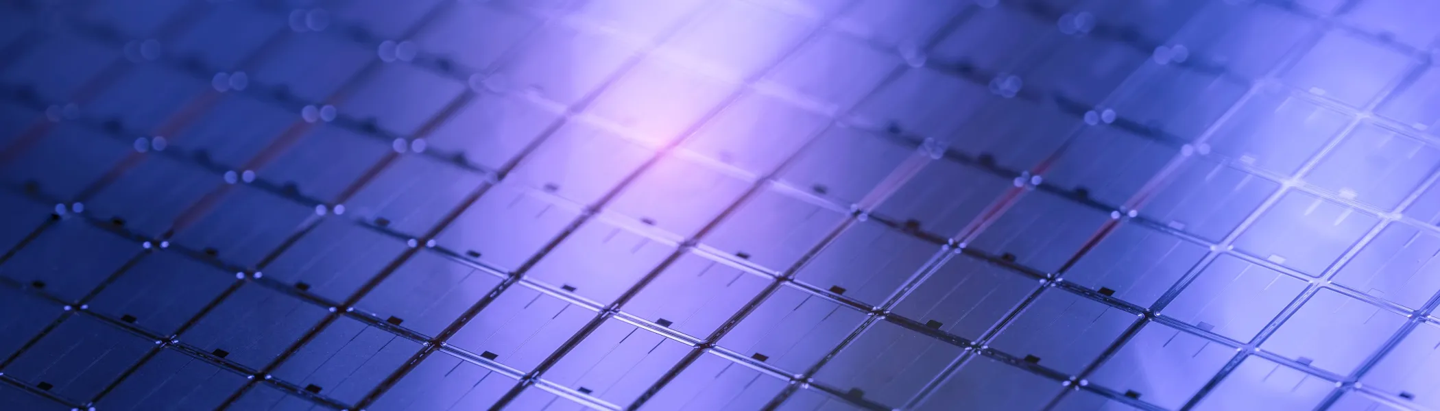
TTV Optimization in Wet Chemical Thinning Using Integrated Metrology
Wet chemical thinning is essential for enhancing substrate uniformity by removing subsurface damage from prior mechanical processing. As semiconductor devices demand thinner substrates with minimal thickness variation, precise control of etching parameters is essential, particularly for power and optical applications. This study examines how integrated metrology and optimized wet etching processes reduce silicon wafer thickness variation across 200-mm wafers. Using NexGen Wafer Systems equipment, variations in etching time, flow rate, and dispenser dynamics minimized rotational asymmetries from prior processes, achieving lower chip thickness uniformity variation. These results provide a foundation for further process automation and optimization in high-volume semiconductor fabrication.
BIOGRAPHY

Jim is a seasoned expert in semiconductor process equipment with over 27 years of specialized experience in Wet Etch and Wet Clean technologies. His career has centered on the design, development, and global deployment of advanced single wafer processing tools, supporting the industry’s most demanding technology nodes.
Prior to entering the semiconductor sector, Jim served 12 years in the U.S. Naval Nuclear Power Program. This rigorous technical foundation in nuclear propulsion systems instilled in him exceptional discipline, problem-solving skills, and a deep appreciation for precision engineering under extreme conditions—qualities that have defined his approach throughout his civilian career.
Transitioning to the semiconductor industry in 1999, Jim quickly established himself as a key contributor in the rapidly evolving field of wet processing. He has played a significant role in the shift from batch to single wafer manufacturing, helping semiconductor manufacturers achieve higher yields, improved uniformity, and tighter process control required for leading-edge nodes. Over the course of his career, Jim has contributed to the design and successful placement of hundreds of single wafer Wet Etch and Wet Clean tools for customers across Asia, Europe, and North America.
His hands-on expertise spans tool design optimization, process integration, customer applications support, and strategic project execution. Jim is widely recognized for his ability to translate complex technical challenges into reliable, high-performance solutions that meet the stringent requirements of advanced logic, memory, and specialty device production.