U.S. National Strategic Plan for Advanced Manufacturing: Virtual Town Hall for Semiconductor Manufacturing Inputs
Join us for a town hall event designed for semiconductor experts to help shape the future of federal research and development in advanced manufacturing. Participants will share insights to help define the priorities for the 2026–2030 National Strategic Plan for Advanced Manufacturing, which guides Federal efforts to enhance the competitiveness of U.S. manufacturing.
The plan is revised every four years to provide new federal priorities in advanced manufacturing research and development, aiming to create jobs, boost economic growth across various sectors, and strengthen national security. This town hall session augments an online Request for Information (RFI), enabling participants to share their views and catalyze deeper input into priority areas.
The White House Office of Science and Technology Policy has posted the complete set of questions in the Federal RegisterHERE.
The National Science and Technology Council’s Subcommittee on Advanced Manufacturing will manage the RFI process, and the NIST Office of Advanced Manufacturing will collect and analyze the information.
Register and tune in on Tuesday, March 17, 2026 at 11am PT / 2pm ET!
Webinar—11am PT / 2pm ET United States
March 17, 2026 | 11am PT / 2pm ET
Ben Kallen
Sr. Manager, Public Policy & Advocacy,
SEMI
Opening Remarks
Robert Rudnitsky, PhD
Division Chief, Strategy and Planning Division,
National Institute of Standards and Technology (NIST)
2026-2030 National Strategic Plan for Advanced Manufacturing
• Importance of U.S. Manufacturing
• Current - Background on 2022-2026 National Strategic Plan
• Future - Stakeholder RFI on 2026-2030 National Strategic Plan
Audience Input on RFI
Join us for a town hall event designed for semiconductor experts to help shape the future of federal research and development in advanced manufacturing.
U.S. National Strategic Plan for Advanced Manufacturing
Virtual Town Hall for Semiconductor Manufacturing Inputs
March 17, 2026
11am PT / 2pm ET
Off
Add to Calendar2026-03-17 00:00:002026-03-17 00:00:00U.S. National Strategic Plan for Advanced Manufacturing: Virtual Town Hall for Semiconductor Manufacturing InputsJoin us for a town hall event designed for semiconductor experts to help shape the future of federal research and development in advanced manufacturing. Webinar—11am PT / 2pm ET United StatesSEMI.org[email protected]America/New_Yorkpublic
America/New_York
The semiconductor industry stands at a generational inflection point with national economic and security priorities converging to define the role of semiconductors for the future. Engaging with lawmakers and policymakers in Washington, DC on trade policy, tariffs, and export controls is of critical importance for the semiconductor and microelectronics industry. If companies do not engage, policy decisions move forward without industry input, which can create missed opportunities and unnecessary risk.
Join us for this expert panel to hear practical guidance and learn how you can ensure your voice is heard by key decision makers.
Navigating the federal policy landscape can seem daunting. Join SEMI Public Policy & Advocacy for an introduction to advocacy with leading firms K&L Gates, Holland & Knight, and Arnold & Porter as featured presenters. These top DC firms will share a concise advocacy and government affairs “101” on trade, tariff, and export control issues as well as an overview of their services and expertise in Washington, DC.
2:30 pm - 3:30 pm
Off
Add to Calendar2026-02-11 14:30:002026-02-11 15:30:00Washington, DC 101: Trade & Export Controls & Semiconductor Policy Insights Webinar - February 11, 2026Navigating the federal policy landscape can seem daunting. Join SEMI Public Policy & Advocacy for an introduction to advocacy with leading firms K&L Gates, Holland & Knight, and Arnold & Porter as featured presenters. These top DC firms will share a concise advocacy and government affairs “101” on trade, tariff, and export control issues as well as an overview of their services and expertise in Washington, DC.DC United StatesSEMI.org[email protected]America/New_Yorkpublic
America/New_York
Join us for an interactive workshop focused on strengthening cybersecurity across the semiconductor manufacturing supply chain. This session will introduce the Semiconductor Manufacturing Cybersecurity Consortium (SMCC) and its standardized Semiconductor Supplier Cybersecurity Assessment (SSCA) framework, a streamlined approach to improving supply chain security assurance. Participants will gain insights into evidence mapping for compliance, explore best practices aligned with NIST’s cybersecurity functions, and engage in discussions with industry experts. Whether you are a semiconductor supplier, compliance professional, or part of the broader manufacturing ecosystem, this workshop offers a unique opportunity to shape future standards and enhance resilience in semiconductor security.
Prerequisite
Download the free SSCA framework document prior to the workshop.
Key Topics
Introduction to Semiconductor Manufacturing Cybersecurity Consortium (SMCC)
Group discussion to feedback on evidence requirements
Open Q&A with cybersecurity and compliance experts
Who Should Attend
Cybersecurity and compliance professionals
Semiconductor Suppliers
Legal and regulatory affairs professionals
Fabless chip designers and foundries
Testing, packaging, design software, R&D tools and IP
Manufacturing/assembly equipment and ancillary fab services
Integrated device manufacturers
Computational Foundry, Bay Campus, Swansea University Swansea SA1 8EN, UK Swansea United Kingdom
10:00 am
-
10:30 pm
Registration
10:30 am
-
11:00 am
Introduction to SMCC and WG3 Objectives
11:00 am
-
12:00 pm
SSCA Questionnaire
12:00 pm
-
12:40 pm
Lunch
12:40 pm
-
1:10 pm
Assurance Mapping
1:10 pm
-
1:40 pm
Feedback and Discussion
1:40 pm
-
2:00 pm
Case Study Presentation
2:00 pm
-
2:30 pm
Group Discussion
2:30 pm
-
2:50 pm
Tea Break
2:50 pm
-
3:30 pm
Feedback Collection
3:30 pm
-
4:00 pm
Closing
Supply Chain Security Assurance of Semiconductor Manufacturing Workshop
10:00 am - 4:00 pm
Off
Add to Calendar2026-03-12 10:00:002026-03-12 16:00:00Supply Chain Security Assurance of Semiconductor Manufacturing UKComputational Foundry, Bay Campus, Swansea University Swansea SA1 8EN, UK Swansea United KingdomSEMI.org[email protected]Europe/Londonpublic
Europe/London
Register Now
Drive Tomorrow’s Critical Policy: Help Shape Key Federal Policy and the Future of the Semiconductor Industry
The semiconductor industry stands at a generational inflection point with national economic and security priorities converging to define the role of semiconductors for the future. While the semiconductor and microelectronics industry is powering the future from AI to next-gen computing, federal policies on trade, tax, workforce and more are also poised to reshape the industry landscape.
The annual DC fly-in is a critical opportunity for SEMI members to advocate for the industry’s top priorities, share real-world insights on how federal policy impacts the industry and highlight the overwhelming contributions SEMI members make to the U.S. economy and national security.
This year, the North American Advisory Board encourages the full SEMI membership to weigh-in with policymakers and share the industry’s most compelling strategies, opportunities, and challenges ahead. As Washington lawmakers assess the political landscape and develop priorities for 2026, the annual fly-in is an opportunity for SEMI members to shape policy on key issues from trade and export controls to talent shortages to supply chain constraints.
Join us as we champion the semiconductor industry in Washington, DC.
TENTATIVE AGENDA
Tuesday, March 3
Breakfast programming and training
Hill meetings
Congressional dinner
Wednesday, March 4
Congressional breakfast
Hill meetings
Hill reception
Thursday, March 5
Roundtable event with CSIS on export controls
Potential government meetings
U.S. Capitol Hill Washington, DC20515 United States
-
Join the North American Advisory Board in Washington, DC for the annual fly-in, bringing together SEMI stakeholders from across the supply chain to engage directly with lawmakers in Congress and help shape the policy priorities that matter most to the semiconductor and microelectronics industry.
SEMI Washington Fly-In
March 3–5, 2026
U.S. Capitol Hill | Washington, DC
Off
Add to Calendar2026-03-03 00:00:002026-03-05 00:00:00SEMI Washington Fly-InJoin the North American Advisory Board in Washington, DC for the annual fly-in, bringing together SEMI stakeholders from across the supply chain to engage directly with lawmakers in Congress and help shape the policy priorities that matter most to the semiconductor and microelectronics industry.U.S. Capitol Hill Washington, DC 20515 United StatesSEMI.org[email protected]America/New_Yorkpublic
America/New_York
Join SEMI and the Environment Risk & Mitigation Reporting Working Group to learn how the semiconductor industry and supply chain is assessing Water Risk, and what steps can be taken to mitigate exposure.
In a collaboration with WaterPlan®, the working group surveyed more than 140 production site and 89 unique water basins to arrive at a water risk assessment for flooding, reputational risk, water quality risk, infrastructure risk and water scarcity risk.The survey found that over 80% of wafer fabrication and 88% of chemical and materials sites face medium-high to high flood risk.
During the webinar experts will provide key insights on key drivers and what is required by risk management teams – both internal and external – for reports and disclosures for:
The Global Reporting Initiative (GRI)
Disclosure Insight Action (CDP)
Task force on Climate-Related Financial Disclosures (TCFD)
The International Sustainability Standards Boards (ISSB)
Sustainability Accounting Standard Board (SASB)
European Sustainability Reporting Standards (ESRS)
Register now to learn more.
Ripple Effects: Water Risk and Resilience Across the Semiconductor Value Chain
8:00 am - 9:00 am
Off
Add to Calendar2025-12-11 08:00:002025-12-11 09:00:00Ripple Effects: Water Risk and ResilienceJoin SEMI and the Environment Risk & Mitigation Reporting Working Group to learn how the semiconductor industry and supply chain is assessing Water Risk, and what steps can be taken to mitigate exposure. In a collaboration with WaterPlan®, the working group surveyed more than 140 production site and 89 unique water basins to arrive at a water risk assessment for flooding, reputational risk, water quality risk, infrastructure risk and water scarcity risk. The survey found that over 80% of wafer fabrication and 88% of chemical and materials sites face medium-high to high flood risk.During the webinar experts will provide key insights on key drivers and what is required by risk management teams – both internal and external – for reports and disclosures for:The Global Reporting Initiative (GRI)Disclosure Insight Action (CDP)Task force on Climate-Related Financial Disclosures (TCFD)The International Sustainability Standards Boards (ISSB)Sustainability Accounting Standard Board (SASB)European Sustainability Reporting Standards (ESRS)Register now to learn more.United StatesSEMI.org[email protected]America/Los_Angelespublic
America/Los_Angeles
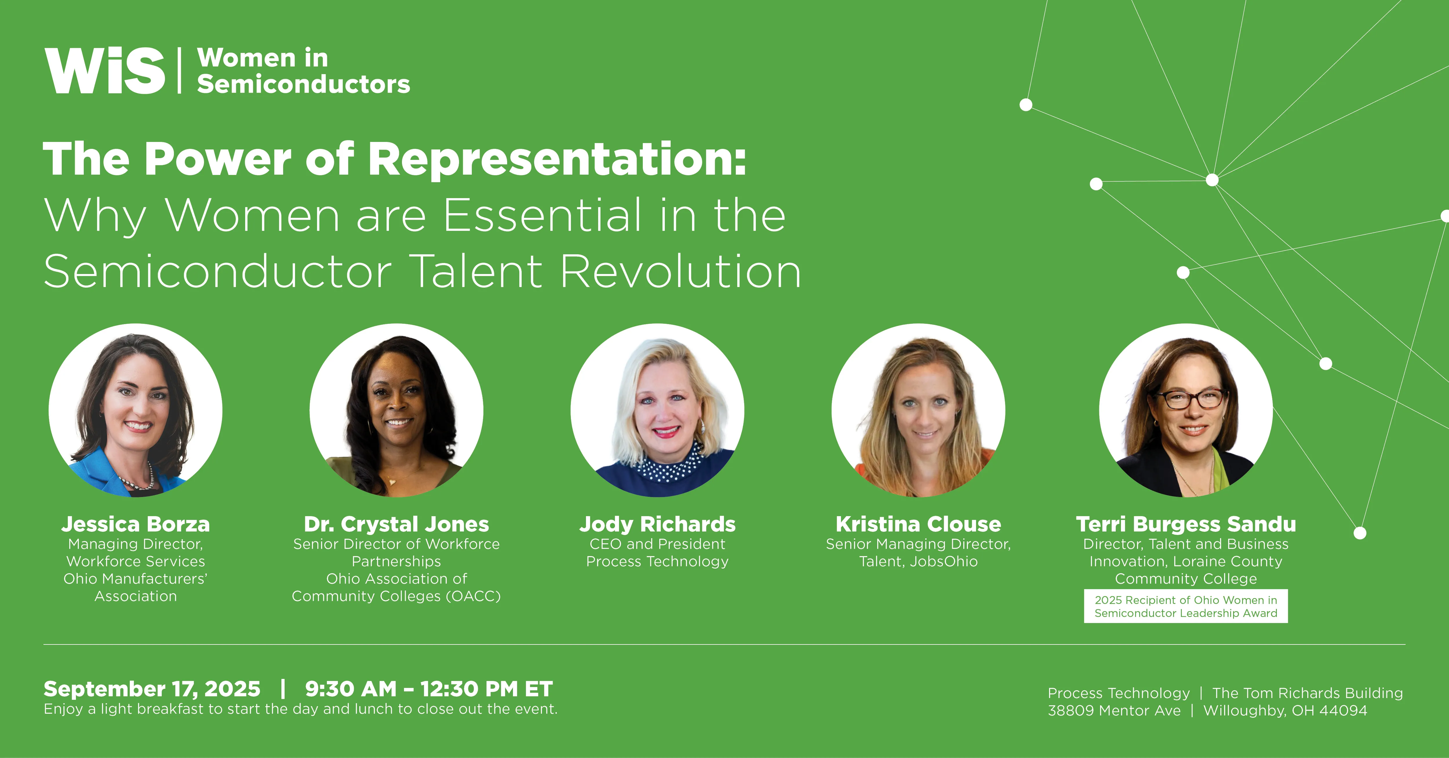
Attending the Women in Semiconductor Conference was an incredibly empowering experience. There is something uniquely impactful about coming together with other women who understand the challenges and opportunities of our industry. The conference created space for honest conversations, meaningful networking, and a sense of community. It is a reminder that we are not alone, and that together, we can drive change and support one another in powerful ways. (WiS 2025 attendee)
Who attends WiS? Company leaders, managers, team members, HR professionals, academia and students. We encourage attendance by everyone who is interested in building a stronger, more dynamic semiconductor ecosystem, and by anyone who is responsible for developing internal or external programs to support women.
Arizona Science Center 600 E Washington Street Phoenix, AZ85004 United States
1:30 pm
-
2:00 pm
Registration & Networking
2:00 pm
-
2:15 pm
Welcome & Introductions
SEMI Foundation Executive Director Michelle Williams, and other invited guests.
2:20 pm
-
3:00 pm
Inspiration Panel: Women Leading the Way in Semiconductors & Beyond
Industry executives share their journeys, leadership lessons, and perspectives on Arizona’s growing role in global technology innovation.
3:05 pm
-
3:40 pm
Educational Panel: Next Gen Women – Powered by Semiconductors
In partnership with Move Over Bob, panelists discuss programs and partnerships that inspire young girls and underrepresented groups to pursue STEM careers.
3:40 pm
-
4:00 pm
Networking Reception
4:00 pm
-
4:30 pm
Speaker Session: Empowered Workplaces – Action into Strategy
Actionable strategies are shared for supporting and retaining talent through flexibility, family support, and adaptable leadership.
4:30 pm
-
5:00 pm
Empowering Women in Semiconductors: Celebrating Fresh Starts and Milestones
Recognizing Fresh Start women upon their completion of a one-year semiconductor apprenticeship program. Celebrating their achievements, growth, and continued journey in an industry that is shaping the future of technology
5:00 pm
-
7:00 pm
STEMinist Mix N Mingle Sponsored by the SEMI Arizona Chapter
Join us for a celebration of women in STEM with mocktails, small bites, and guided networking to support mentorship and collaboration—plus a special private viewing in the Dorrance Dome at the Arizona Science Center.
Arizona is quickly becoming one of the nation’s top hubs for semiconductor innovation—and women are at the center of this transformation. Women in Semiconductors: Empowerment in Action celebrates the achievements, leadership, and impact of women across the semiconductor and technology industries while equipping attendees with actionable insights to drive growth, opportunity, and progress in the workplace and beyond.
This half-day program celebrates and empowers women in STEM while highlighting Arizona’s leadership in the nation’s expanding semiconductor sector. Empowerment in Action: To the Workplace & Beyond brings together industry professionals, educators, and students for an afternoon of storytelling, insight, and collaboration.
Through panels, speaker sessions, and interactive discussions, attendees will hear firsthand from women leading the way in science and technology—sharing how they’ve built their careers, navigated challenges, and contributed to Arizona’s growing technology landscape.
The day concludes with the STEMinist Mix N Mingle—a relaxed networking session featuring mocktails, small bites, and engaging activities designed to spark mentorship and build community connections.
REGISTRATION IS NOW CLOSED.
To receive information about Women in Semiconductors events, make sure to complete our interest form.
Off
Add to Calendar2025-12-02 00:00:002025-12-02 00:00:002025 Semiconductor Innovation and Intelligent Application Summit (SIIAS)New Territories Hong Kong ChinaSEMI.org[email protected]America/Los_Angelespublic
Smart Sensors and Edge Intelligence for Advanced Process Control
Overview: Explore the latest sensor technologies—optical, thermal, vibration, and chemical—and how embedded AI at the edge enables real-time control loops for critical wafer fab processes. Includes case studies on inline metrology and adaptive control.
Key Topics: Sensor fusion and calibration, Edge inference for process drift detection, Integration with APC and FDC system
8:00 am
-
8:45 am
Registration & Breakfast
8:45 am
-
8:55 am
Anshu Bahadur
SEMI
Day 1 - Welcome All
Welcome & SEMI Manufacturing Coalitions Overview
8:55 am
-
9:30 am
Russell Dover
General Manager, Service Product Line
LAM
Keynote: Vision – Edge Inference – Process Control, APC, FDC
9:30 am
-
9:55 am
James Bramante
Senior Data Scientist
INFICON
Managing Edge AI for Smart Sensor Process Control
9:55 am
-
10:20 am
Robert Hillinger
Industry Leader Semiconductor
Kistler
Advanced Process Control with Piezoelectric Sensor Fusion for Semiconductor Manufacturing
10:20 am
-
10:35 am
Coffee Break
10:35 am
-
11:00 am
Chris Dickens
Application Eng
Beckhoff Automation
A Unified Industrial Platform for Production-Ready AI
11:00 am
-
11:25 am
Gokul Sathya
Research Scientist
Siemens
Physical AI on the Manufacturing Floor: From Virtual Commissioning to Deployment
11:25 am
-
11:50 am
Aumkar Renavikar
Chief Product Officer, Co-Founder & CTO
Parallax Worlds
Intelligent Robots & Digital Twins for Advanced Manufacturing
11:50 am
-
12:05 pm
Chakravarthy Elumalai
CTO
Ray Vector
Sensor as the Eyes and Ears of AI
12:05 pm
-
1:00 pm
Networking Lunch
Afternoon, Day 1: March 18th, 2026
.
Yield Enhancement through Edge-Driven Defect Detection and Classification
Overview: Present how edge AI models process sensor and image data to identify yield-impacting defects early in the process. Discuss virtual metrology, anomaly detection, and feedback loops for yield optimization.
Key Topics: Real-time defect classification, Sensor-based yield prediction, Integration with SPC and yield dashboards
1:00 pm
-
1:05 pm
Karim Somani
SEMI
SEMI Fab Owners Alliance (FOA)
1:05 pm
-
1:35 pm
Surya Kalidindi
Co-Founder
Multiscale
Physics-Aware AI for Semiconductor Manufacturing Process Optimization: Deployed Systems and the Edge AI Frontier
1:35 pm
-
2:00 pm
Maryia Kurdina
AI R&D Group Leader, Technology & AI Design Research Center
TEL
Real-Time, Tool-Independent Health Monitoring Using Gaussian Process Confidence Bands on Sensor Signals
2:00 pm
-
2:25 pm
Avni Agarwal
Co-Founders & CTO
SixSense
Applications of AI-Based Defect Classification for Yield Improvement: From FEOL (Front end-of line) in Fabs to Assembly and Test
2:25 pm
-
2:40 pm
Coffee Break
2:40 pm
-
3:05 pm
Arjun Hegde
Senior Application Engineering Manager
KLA
Edge-Driven Yield Learning: Real-Time Deep Learning and HAR Defect Discovery in Advanced E-Beam Architectures
3:05 pm
-
3:30 pm
Prasad Bachiraju
Senior Director, Business Development
Onto Innovation
Reducing Rework and Boosting Fab Capacity with Edge AI and Metrology-Driven Predictive Analytics
3:30 pm
-
3:55 pm
Danny Krastev
Full Stack AI Developer
Microtronic
Overcoming the challenges of AI defect detection and classification of semiconductor macro defects
3:55 pm
-
4:20 pm
Chengli He
Industry Manager
MathWorks
From Data to Decisions: Edge AI for Yield, Defect Detection, and Predictive Insights
4:20 pm
-
4:35 pm
Stephen March
Semiconductor Leader
Schneider
Software Defined Industrial Automation: A Blueprint for AI-Ready, Real-Time Edge Operations in Semiconductor Manufacturing
4:35 pm
-
6:35 pm
Reception
Morning, Day 2: March 19th, 2026
Autonomous WIP Movement: Robots, Sensors, and Edge AI Coordination
Overview: Dive into next-gen clean rooms – how intelligent robotics & AI‑enabled inspection elevate yield, reliability & efficiency.
Key Topics: Sensor-guided AGVs and AMRs, AI-based path optimization, Interoperability with fab logistics systems
8:00 am
-
8:45 am
Registration & Breakfast
8:45 am
-
8:55 am
Paul Carey and Melissa Grupen-Shemansky
SEMI
Day 2 - Welcome All
Day 1 Overview & MSIG Overview
8:55 am
-
9:30 am
Carlos O’Farrill
Global Key Account Manager
KUKA
Keynote: Smarter Fabs in Motion: How Edge AI and Sensor Networks Drive Autonomous Material Handling
9:30 am
-
9:55 am
Vidya Vijay
Director, Business Development, Growth & Strategy
Nordson
Precision, Automation, and Beyond: The Role of Advanced Sensors in the Evolution of Semiconductor Manufacturing for effective Tool set-up, Predictive and Preventative Maintenance
9:55 am
-
10:20 am
Joseph Tsao
US Sales Director
Solomon 3-D
Perception-Enabled Assurance of Semiconductor Manufacturing Systems
10:20 am
-
10:35 am
Coffee Break
10:35 am
-
11:00 am
Murali Krishna
Vice President of Products
Minds.ai
Using Edge AI models and Deep RL to improve yield, tool availability, and fab performance
11:00 am
-
11:25 am
Michael Bowcutt
Director of Sales Engineering
CamLine
Solving the Interoperability Gap: Orchestrating and Emulating Mixed-Fleet Robotics for High-Yield Fabs
11:25 am
-
11:50 am
Greg Berger
Solution Consultant
Rockwell Automation
Smart Modular Conveyance, the first step towards Autonomous Operations in Analog & Legacy fabs
11:50 am
-
12:15 pm
Brian Zmikly
Sr. Director, US Enterprise & Government Sales, 5G Acceleration
Verizon
The 5G Fabric: Leveraging Next Gen Connectivity to Enable Automation and Intelligence
12:15 pm
-
12:30 pm
Anshu Bahadur
SEMI
Robots in the Cleanroom: Future of Automation in Semiconductor Manufacturing
12:30 pm
-
1:30 pm
Networking Lunch
Afternoon, Day 2: March 19th, 2026
Predictive Maintenance at the Edge: From Vibration to Vision
Overview: Highlight how edge-deployed AI models use sensor data (vibration, acoustic, thermal, visual) to predict equipment failures before they occur. Showcase deployment strategies and ROI from reduced downtime.
Key Topics: Edge analytics for tool health, Federated learning across equipment fleets, Maintenance scheduling optimization
1:30 pm
-
2:05 pm
James Bramante
Senior Data Scientist
INFICON
Keynote: Predictive Maintenance at the Edge - AI Enabling PdM
2:05 pm
-
2:30 pm
Michael Passow
AI Semiconductor Factory Automation Program Manager
IBM
Edge AI–Enabled Predictive Maintenance: Closing the Loop Between Equipment Health and Fab Operations
2:30 pm
-
2:55 pm
Mauro Riboni
Technical lead – Alliance & Partnership
Bosch
The Edge Revolution: Predictive Maintenance Reborn with Edge AI
2:55 pm
-
3:20 pm
Paul Johnson
Senior Manager – Digital Transformation
Edwards
The Challenge Of AI At The Edge – Making Use Of Advanced Sensors
3:20 pm
-
3:35 pm
Coffee Break
3:35 pm
-
4:00 pm
Sainyam Galhotra
Co-founder & Faculty, Cornell University
Third AI Automation
Edge-based Defect Detection and Predictive Maintenance in Semiconductor Manufacturing
4:00 pm
-
4:25 pm
Sundeep Ahluwalia
Chief Product Officer
TDK SensEI
Edge AI: The Future of Industrial Machine Health Monitoring
4:25 pm
-
4:50 pm
Kelli Case
Business Development Director, Senseye Predictive Maintenance
Siemens
How AI‑based Maintenance Can Reshape Semiconductor Operations By Cutting Downtime By Up To 50%
Unlocking Smarter, More Autonomous Fabs with Edge AI
As semiconductor fabs strive for higher yield, uptime, and efficiency, AI at the edge is becoming central to semiconductor manufacturing. Modern edge devices combine advanced sensors with embedded AI to monitor equipment, optimize energy, and detect anomalies in real time - without relying on the cloud.
This workshop will explore how AI-driven sensors and edge intelligence, integrated with IoT, 5G, and AI accelerators, enable scalable, resilient, and intelligent solutions tailored for semiconductor manufacturing. Learn how these technologies support:
Predictive maintenance to prevent downtime
Adaptive process automation for maximum efficiency
Real-time decision-making at the source of data generation
Join us to see how the convergence of sensors, edge AI, and connectivity is unlocking the next era of smart manufacturing.
Smarter Sensors, Smarter Fabs: AI at the Edge in Semiconductor Manufacturing
In-Person Workshop | March 18-19, 2026 | Milpitas, CA
Off
Add to Calendar2026-03-18 00:00:002026-03-19 00:00:00Smarter Sensors, Smarter Fabs: AI at the Edge in Semiconductor ManufacturingUnlocking Smarter, More Autonomous Fabs with Edge AIAs semiconductor fabs strive for higher yield, uptime, and efficiency, AI at the edge is becoming central to semiconductor manufacturing. Modern edge devices combine advanced sensors with embedded AI to monitor equipment, optimize energy, and detect anomalies in real time - without relying on the cloud.This workshop will explore how AI-driven sensors and edge intelligence, integrated with IoT, 5G, and AI accelerators, enable scalable, resilient, and intelligent solutions tailored for semiconductor manufacturing. Learn how these technologies support:Predictive maintenance to prevent downtimeAdaptive process automation for maximum efficiencyReal-time decision-making at the source of data generationJoin us to see how the convergence of sensors, edge AI, and connectivity is unlocking the next era of smart manufacturing.Milpitas, CA United StatesSEMI.org[email protected]America/Los_Angelespublic
America/Los_Angeles
On Demand
A digital twin is a computer representation of the structure, context, and behavior of physical systems, which are critical components in the optimization of computational systems, accurately representing physical systems and processes. A Digital Twin can be used to reduce or eliminate iterative physical experiments needed for optimization, thereby enhancing yield, saving time, and resources. Semiconductor manufacturing involves numerous complex steps, where accurate control of each step is crucial to achieving the overall manufacturing yield and minimizing variations in device characteristics. The complexity of the manufacturing processes' flows limits flexibility for testing novel approaches. Unit processes can be based on first-principal models (physics-based), data-based models, or hybrid models combining both approaches when possible. Fabrication processes in the cleanroom and on printed electronics tools are often a function of time-varying parameters, including those of the equipment, environment, and materials. The parameters often have co-dependencies across different process steps and tool sets.
This course will cover the necessary material to create DNN-based Digital twins for nanofabrication processes in cleanrooms. The course will include experimental details for data preparation, data processing, training models, and use case demonstrations. Nanofabrication process equipment can inherently have millions of internal variables and can learn from datasets, providing a robust and complementary approach to traditional feedback control and process stabilization methods. The included Digital Twin modes are developed using images (CD-SEMs, optical images), time history data (Optical Emission Spectroscopy), and textual process information (recipes and materials). The course will include: (1) Approaches to preprocess image data and create learning-based models, (2) using DNN-based domain translation for learning to predict the DUV nanolithography and ICP Plasma Etch, (3) virtual metrology methods for quantification of learning outcomes, and (4) developing a new class of process-aware DNN-based digital twins.
ABOUT THE SPEAKERS
Benyamin Davaji, PhD Benyamin Davaji is an Assistant Professor in the Electrical and Computer Engineering Department at Northeastern University. His research focuses on integrated microsystems with an emphasis on sensing and computation using mechanical waves, acoustic/ultrasound transducers, bio-interfaces, and microcalorimetry. He also applies data-guided methods to nanofabrication process development and semiconductor manufacturing. Dr. Davaji earned his PhD in Electrical and Computer Engineering from Marquette University in 2016 and later served as a post-doctoral associate at Cornell University’s School of Electrical and Computer Engineering.
Peter Doerschuk, PhD
Peter Doerschuk, Professor at Cornell University since 2006, previously served on the Purdue faculty in Electrical and Computer Engineering and Biomedical Engineering. He earned B.S., M.S., and Ph.D. degrees in Electrical Engineering from MIT, an M.D. from Harvard Medical School, and completed training at Brigham and Women’s Hospital and a postdoc at MIT. His research applies computational nonlinear stochastic systems to biology and medicine, spanning viral 3-D structure determination using electron microscopy and x-ray scattering, to nonlinear models of ethanol pharmacokinetics that enable sensor processing, pattern recognition, and individualized physiological analysis.
Join us for this engaging Master Class with Benyamin Davaji, PhD, Assistant Professor of Electrical and Computer Engineering at Northeastern University and Peter Doerschuk, Professor of Electrical and Computer Engineering and Biomedical Engineering at Cornell University, as they explore the role of digital twin models in advancing semiconductor manufacturing. The masterclass will highlight how data-guided methods and computational modeling are transforming unit process development, driving efficiency and innovation across the semiconductor industry. With expertise spanning microsystems, acoustic transducers, and nanofabrication, the speakers will provide insights into how digital twins can bridge research and production to accelerate breakthroughs in semiconductor technology.
Digital Twin Models for Semiconductor Manufacturing Unit Process
Flexible Electronics Master Class #27
10:00 am - 12:00 pm
Off
Add to Calendar2025-11-05 10:00:002025-11-05 12:00:00FEMC#27 Digital Twin Models for Semiconductor Manufacturing Unit ProcessJoin us for this engaging Master Class with Benyamin Davaji, PhD, Assistant Professor of Electrical and Computer Engineering at Northeastern University and Peter Doerschuk, Professor of Electrical and Computer Engineering and Biomedical Engineering at Cornell University, as they explore the role of digital twin models in advancing semiconductor manufacturing. The masterclass will highlight how data-guided methods and computational modeling are transforming unit process development, driving efficiency and innovation across the semiconductor industry. With expertise spanning microsystems, acoustic transducers, and nanofabrication, the speakers will provide insights into how digital twins can bridge research and production to accelerate breakthroughs in semiconductor technology.United StatesSEMI.org[email protected]America/Los_Angelespublic
America/Los_Angeles
Watch On-Demand