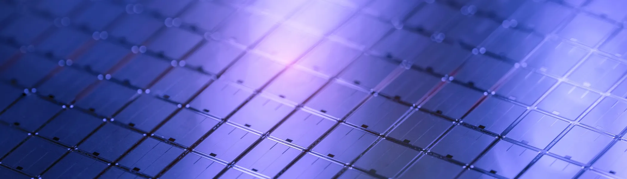
Silicon-Germanium Etchants with Excellent Silicon and Silicon Oxide Compatibility for Advanced Semiconductor Devices
This presentation highlights recent advances in formulated chemistries for silicon–germanium (SiGe) etching that offer high compatibility with silicon (Si) and silicon oxide (SiOx)—a critical requirement in advanced semiconductor device fabrication. As device architectures continue to scale to smaller nodes and evolve toward complex three‑dimensional (3D) structures with high aspect ratios, high‑selectivity etchants (HSE) have become essential for achieving precise patterning and optimal electrical performance. Conventional H2O2‑based solutions, however, are unable to deliver the required selectivity between SiGe, Si, and SiOx.
To address these limitations, we developed multi‑component formulated chemistries designed to tune etch rates and enhance selectivity. By incorporating a novel silicon oxidizer that selectively interacts with SiGe and employing a component to dissolve the oxidized SiGe, the new formulations minimize silicon damage while enabling effective SiGe removal. Additional silicon inhibitors further suppress Si etching, and careful selection of pH adjusters provides strong protection for SiOx surfaces. Overall, these results offer practical strategies for overcoming key selective etching challenges in advanced semiconductor manufacturing and support the continued advancement of device performance.
BIOGRAPHY
Chun‑Ren (Jack) is a High Selectivity Etchant (HSE) R&D expert at Qnity Electronics within the Advanced Cleans and Slurry Technologies (ACST) organization. He has more than six years of experience in advanced semiconductor processing and currently focuses on developing novel formulated etchants for silicon (Si), silicon–germanium (SiGe), and various metal etchants. His work centers on achieving stringent materials selectivity and precise etch‑profile control required for high‑aspect‑ratio (HAR) device architectures.
Beyond wet etch technologies, Jack also has extensive experience in advanced lithography and photovoltaic semiconductor materials (silicon-based and perovskite-based). He holds a Ph.D. from the University of Manchester (UK), where he specialized in materials chemistry and photon physics with multiple journal publications. Dr. Ke also holds a few granted patents in nanotechnology area.