downloadGroupGroupnoun_press release_995423_000000 copyGroupnoun_Feed_96767_000000Group 19noun_pictures_1817522_000000Member company iconResource item iconStore item iconGroup 19Group 19noun_Photo_2085192_000000 Copynoun_presentation_2096081_000000Group 19Group Copy 7noun_webinar_692730_000000Path
Skip to main content
Default Banner Image

Russia

DRESDEN, Germany — June 5, 2024 —The SEMI 3D & Systems Summit, taking place from 12-14 June, 2024 in Dresden, will feature the forefront of technological integration. Themed Heterogeneous Systems for the Intelligently Connected Era, the summit will unravel the intricate web of collaboration among components driving the next wave of innovation. From artificial intelligence algorithms to sensor data processing, attendees will deep dive into the dynamic framework enabling decision-making and real-time applications in an increasingly connected world. Registration is open.

"SEMI Europe looks forward to welcoming leading experts in Dresden. With exceptional speakers and a brand-new exhibition, the Summit offers insights into cutting-edge heterogeneous integration innovations essential for semiconductor applications, driving the advancement of intelligent systems," said Laith Altimime, President of SEMI Europe.

This year’s SEMI 3D & Systems Summit will present a broad scope of topics including:

  • AI as a Driver to Grow 3D Technology Implementation
  • Accelerating the AI Economy through Heterogeneous Integration
  • Heterogeneous Integration for Photonics Applications
  • Technology and Market Updates for 2.5D & 3D Packaging for Heterogeneous Integration
  • Design and Technologies of Chiplet System Architectures
  • Hybrid Bonding Technologies for Advanced 3D Integration
  • Manufacturing Innovation for 3D Integration

Featured Speakers 

Global Leaders to Present 

3D & Systems Summit presenters include experts from global leaders:

  • Adeia
  • ANSYS, Inc.
  • ASE, Inc. 
  • CEA-Leti
  • Comet Yxlon
  • EPIC
  • European Commission
  • EV Group
  • Fraunhofer IZM
  • HEIDENHAIN
  • imec
  • KLA Corporation
  • Lam Research
  • MKS-Atotech
  • NVIDIA
  • PDF Solutions
  • Siemens EDA
  • Silicon Saxony
  • SPTS Technologies
  • STMicroelectronics
  • SUSS MicroTec
  • TechSearch International, Inc.
  • Tokyo Electron Limited
  • Yole Group

Networking 

This year’s networking reception will take place at the Hilton Dresden on the first day of the event, and the annual networking dinner will be held on the Elbe River cruise on the second day of the summit.

Networking Dinner Cruise registration is reserved exclusively for 3D & Systems Summit 2024 participants. Guests may register their spouse for dinner by completing the spouse registration form.

Exhibition

The most prominent names in 3D integration microelectronics manufacturing will showcase their latest products and technologies at the new exhibition area. Exhibitors include: Adeia, ASE, Inc., ASMPT AMICRA, Besi, CEA-Leti, Comet Yxlon, Confovis, European Chips Diversity Alliance, European Chips Skills Academy, EV Group, Fraunhofer IZM-ASSID, HEIDENHAIN, HiCONNECTS, Lam Research, ProSys, Renishaw, SET Corporation, Tokyo Electron Limited and Wooptix.

To reserve an exhibition space, contact [email protected].

3D & Systems Summit Premium Sponsors

For more details, please visit the 3D & Systems Summit 2024 website and connect with SEMI Europe on X or LinkedIn @SEMIEurope (#3DSummit).

About SEMI
SEMI® is the global industry association connecting over 3,000 member companies and 1.5 million professionals worldwide across the semiconductor and electronics design and manufacturing supply chain. We accelerate member collaboration on solutions to top industry challenges through Advocacy, Workforce Development, Sustainability, Supply Chain Management and other programs. Our SEMICON® expositions and events, technology communities, standards and market intelligence help advance our members’ business growth and innovations in design, devices, equipment, materials, services and software, enabling smarter, faster, more secure electronics. Visit www.semi.org, contact a regional office, and connect with SEMI on LinkedIn and X to learn more.

Association Contacts

Serena Brischetto/SEMI Europe
Phone: +49 30 3030 8077-11
Email: [email protected]

Michael Hall/SEMI US
Phone: 1.408.943.7988
Email: [email protected]

Initial Course Programs Designed to Meet Rising Industry Demand for Technicians

MILPITAS, Calif. — May 14, 2023 — Aiming to help the global semiconductor industry address its talent gap by training and upskilling workers, SEMI today announced that its SEMI University™ learning platform now offers online course certification programs designed to fast-track semiconductor career development. Tailored to help meet burgeoning industry demand for technicians, the first two SEMI University Semiconductor Certification Programs are designed for new talent seeking rewarding careers in the industry and experienced workers looking to keep their skills current.

“With semiconductor manufacturers investing heavily in new fabs backed in part by government incentives, SEMI projects the global industry will need 1 million new workers worldwide by 2030 to support the chipmaking expansion,” said Shari Liss, Executive Director of the SEMI Foundation, which drives the SEMI Workforce Development program. “Technicians are in the highest demand, accounting for roughly 40% of the semiconductor workforce worldwide. The SEMI University Certification Program will help meet the industry’s pressing need for a diverse range of training and certification programs to close the talent gap.”

“SEMI University’s new Semiconductor Certification Programs give the industry a fast way to train new talent while enabling current workers to keep pace with its expanding skills requirements,” said SEMI University Director Naresh Naik. “The first two certification programs address critical technician roles. We look forward to adding new certifications to support the industry’s growing workforce needs and career development for our learners.”

The SEMI University Semiconductor Certification Programs include:

  • The Semiconductor Technician Certification equips new semiconductor industry workers with the skills necessary to excel in chip manufacturing. The certification program provides comprehensive training in the semiconductor process and on-the-job tasks. Courses cover the function of semiconductors and their manufacture, how electrical circuits work and the physical laws that apply to electrical current, as well as the various applications of electrical testing equipment.
  • The Pneumatics/Hydraulics Technician Certification covers the use of vacuum technology in pneumatic systems and hydraulics theory. Courses address the properties of gases and vacuums, how various vacuum types are generated, and hydraulic systems and their components including actuators. The curriculum also compares hydraulic and pneumatic systems.

About SEMI University
The SEMI University learning platform offers more than 575 online courses tailored for the semiconductor industry, providing easy-to-use online training in multiple languages for employees ranging from recently hired facility operators to experienced technicians, engineers and non-technical staff. SEMI U also offers in-person trainings. See the SEMI University Course Calendar.

About the SEMI Workforce Development Program
SEMI has offered in-person training and technology trend for updates more than 50 years, and it hosts webinars covering SEMI standards, market dynamics and semiconductor manufacturing and design best practices. SEMI University builds on this experience and adds to the association’s holistic Workforce Development program offered by the SEMI Foundation.

The non-profit arm of SEMI, the SEMI Foundation works to increase awareness of semiconductor industry careers, connect member companies with university students for mentoring and internships, attract and train military veterans, and develop a more diverse and inclusive workforce. Learn more about semiconductor industry career paths at the SEMI Foundation Career Portal.

About SEMI
SEMI® is the global industry association connecting over 3,000 member companies and 1.5 million professionals worldwide across the semiconductor and electronics design and manufacturing supply chain. We accelerate member collaboration on solutions to top industry challenges through Advocacy, Workforce Development, Sustainability, Supply Chain Management and other programs. Our SEMICON® expositions and events, technology communities, standards and market intelligence help advance our members’ business growth and innovations in design, devices, equipment, materials, services and software, enabling smarter, faster, more secure electronics. Visit www.semi.org, contact a regional office, and connect with SEMI on LinkedIn and X to learn more.

Association Contact

Michael Hall/SEMI US
Phone: 1.408.943.7988
Email: [email protected]

The European Chip Skills Academy (ECS Academy) Connects Students with Microelectronics Studies to Help Build Talent Pipeline

BRUSSELS, Belgium – May 16, 2024 – University students will connect with professors to explore semiconductor learning paths and employment opportunities at the European Chip Skills Academy Summer School, August 18-23, 2024 in Bologna, Italy. Supported by SEMI and held in collaboration with AENEAS, EPoSS, and Inside, the event is integral to the European Chips Skills Academy, an EU-funded project coordinated by SEMI Europe. The event will be held at the University Residential Centre, University of Bologna, Bertinoro, Italy. Registration is open.

The ECS Academy, funded through the Erasmus+ program, aims to foster dialogue, strategic planning, and actionable steps to help grow the microelectronics industry workforce.

The Summer School will serve as a key initiative of the ECS Academy for 2024, offering insights into current microelectronics technologies and anticipated future applications across the semiconductor value chain.

Summer School Key Topics

  • Semiconductor Technology
  • Integrated Circuits Design
  • Digital Systems and Embedded Intelligence
  • Integration, including Packaging and MEMS Technology

Other Event Highlights

  • Networking Reception – Meet with peers and industry experts to explore semiconductor industry career paths.
  • Meet like-minded students – Interact with peers with similar interests and motivations.
  • Explore Bologna: Admire the city’s unique architecture, and in particular the red tiled rooftops.

Enrollment Criteria

The initiative is designed for STEM undergraduates’ students in the following categories:

The Summer School will be complimentary. Some participants may qualify for a travel reimbursement of up to 600 EUR.

Student selection will be based on the applicant’s CV, a motivation letter, recommendation letters, and academic transcripts. The selection process will take into account gender and geographical balance to ensure diverse student backgrounds.

Applications should be submitted by May 19, 17:00 CEST. Selected students will be notified on June 15, 2024.

For more details, please visit the Summer School webpage and connect with SEMI Europe on X or LinkedIn @SEMIEurope and with ECSA on X and LinkedIn (#summerschool #ECSA #talent #microelectronics).


About SEMI
SEMI® is the global industry association connecting over 3,000 member companies and 1.5 million professionals worldwide across the semiconductor and electronics design and manufacturing supply chain. We accelerate member collaboration on solutions to top industry challenges through Advocacy, Workforce Development, Sustainability, Supply Chain Management and other programs. Our SEMICON® expositions and events, technology communities, standards and market intelligence help advance our members’ business growth and innovations in design, devices, equipment, materials, services and software, enabling smarter, faster, more secure electronics. Visit www.semi.org, contact a regional office, and connect with SEMI on LinkedIn and X to learn more.

Association Contacts

Serena Brischetto/SEMI Europe
Phone: +49 30 3030 8077-11
Email: [email protected]

Michael Hall/SEMI US
Phone: 1.408.943.7988
Email: [email protected]

MUNICH, Germany ─ May 21, 2024 ─ SEMI Europe today announced the opening of the Call for Abstracts for SEMICON Europa 2024, to be held November 12-15 at Messe München in Munich, Germany. Selected speakers will share their expertise at the Advanced Packaging Conference (APC), Fab Management Forum (FMF), MEMS & Imaging Sensors Summit and during presentations on the show floor.

Europe’s premier event connecting the entire electronics design and manufacturing supply chain, SEMICON Europa 2024 will gather industry-leading experts and innovators to explore cutting-edge technologies, materials, and process advancements driving the digital transformation and growth in the semiconductor industry. The exhibition and conference will be co-located with electronica.

Call for Abstracts – Events

Advanced Packaging ConferenceChiplets and Heterogenous Integration: The Next Frontier in Performance and Efficiency

The emergence of new types of neural networks like ChatGPT and other AI applications is driving unprecedented demand for high-performance computing (HPC) and innovations in advanced packaging – including for chiplets – heat dissipation, miniaturization, material integration, and power optimization. Abstracts on topics including growth through innovation, developments in design, manufacturing efficiency, and testing systems are invited.

Fab Management ForumIndustry Meets Innovative Ideas

Geared for fab managers, the Fab Management Forum will focus on optimizing next-generation core technologies such as SiC, photonics, and quantum computing to support industry growth. The forum will explore advancements in smart manufacturing solutions that leverage AI-driven tools for efficiency gains to address Europe's environmental sustainability goals and mitigate semiconductor industry-related environmental risks.

MEMS & Imaging Sensors Summit MEMS and Imaging Young Talent

Entrepreneurs, start-up companies, and graduates will showcase their research and early-stage products to MEMS and imaging sensors technologists. Topics of interest include MEMS technologies, new applications and use cases, advancements in MEMS and sensors technology and materials, MEMS-photonics co-integration, and imaging technologies focused on new sensor applications, materials, and architectures.

Pre-recorded Innovation PresentationsInnovation and Collaboration: Powering Sustainable Exponential Growth

SEMI Europe will also highlight microelectronics and semiconductors innovations in short pre-recorded messages, pitches and product announcements by technologists. The videos will be aired on SEMICON Europa 2024 main stages during networking sessions and on the final day of the event.

Presentation abstracts, biographies and headshots must be submitted in English on the SEMICON Europa 2024 Call for Abstracts webpage by June 17, 2024. Selected presenters will be notified in August 2024.

For more details, please visit the SEMICON Europa 2024 website and connect with SEMI Europe on X or LinkedIn @SEMIEurope (#SEMICONEuropa).

SEMICON Europa Premier Sponsors

  • Platinum: Comet Yxlon, Edwards, Inficon and Siemens
  • Gold: KLA+, Schneider Electric and Synopsys
  • Silver: Adeia, Honeywell and Semilab
  • Event sponsors: ASE, Inc., IBM, MKS-Atotech, Screen and Watlow

About SEMI
SEMI® is the global industry association connecting over 3,000 member companies and 1.5 million professionals worldwide across the semiconductor and electronics design and manufacturing supply chain. We accelerate member collaboration on solutions to top industry challenges through Advocacy, Workforce Development, Sustainability, Supply Chain Management and other programs. Our SEMICON® expositions and events, technology communities, standards and market intelligence help advance our members’ business growth and innovations in design, devices, equipment, materials, services and software, enabling smarter, faster, more secure electronics. Visit www.semi.org, contact a regional office, and connect with SEMI on LinkedIn and X to learn more.

Association Contacts

Maria Daniela Perez/SEMI Europe
Phone: +49 160 2562977
Email: [email protected]

Michael Hall/SEMI US
Phone: 1.408.943.7988
Email: [email protected]

 MILPITAS, Calif. – May 14, 2024 – The global semiconductor manufacturing industry in the first quarter of 2024 showed signs of improvement with an uptick in electronic sales, stabilizing inventories and an increase in installed wafer fab capacity, SEMI announced today in its Q1 2024 publication of the Semiconductor Manufacturing Monitor (SMM) Report, prepared in partnership with TechInsights. Stronger industry growth is expected in the second half of the year.

In Q1 2024, electronic sales rose 1% year-over-year (YoY), with Q2 2024 forecast to register a 5% YoY increase. IC sales posted robust 22% YoY growth in Q1 2024 and are expected to surge 21% in Q2 2024 as sSEMI in Partnership with TechInsights
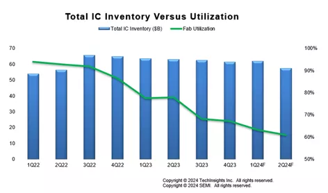
hipments of high-performance computing (HPC) chips increase and memory pricing continues to improve. IC inventory levels stabilized in Q1 2024 and are expected to improve this quarter.

Installed wafer fab capacity continues to increase and is projected to exceed 40 million wafers per quarter (in 300mm wafer equivalent), rising 1.2% in Q1 2024 with an expected 1.4% uptick in Q2 2024. China continues to log the highest capacity growth among all regions. However, fab utilization rates, particularly for mature nodes, remain a concern with little signs of recovery expected in the first half of 2024. Memory utilization rates were lower than expected in Q1 2024 due to disciplined supply control.

In line with fab utilization trends, semiconductor capital expenditures remain conservative. After falling 17% YoY in Q4 2023, capital expenditures continued to pull back 11% in Q1 2024 before eking out an expected 0.7% gain in Q2 2024. Sequentially in Q2 2024, the trend is turning positive with an expected 8% increase in memory-related capital expenditures as they see slightly stronger growth than non-memory segments.

“Demand in some semiconductor segments is recovering, but the pace of recovery is uneven,” said Clark Tseng, Senior Director of Market Intelligence at SEMI. “AI chips and high-bandwidth memory are currently among devices in the highest demand, leading to increased investment and capacity expansion in these areas. However, the impact of AI chips on IC shipment growth remains limited due to their reliance on a small number of key suppliers.”

“Semiconductor demand in the first half of 2024 is mixed, with memory and logic rebounding due to surging generative AI demand,” said Boris Metodiev, Director of Market Analysis at TechInsights. “However, analog, discrete, and optoelectronics have experienced a slight correction due to the slow recovery of the consumer market coupled with a pullback in demand from the automotive and industrial markets.”

“A full-on recovery is likely to take hold in the second half of the year with the projected boost in consumer demand by AI’s expansion to the edge,” Metodiev said. “Additionally, the automotive and industrial markets are expected to return to growth in the latter part of the year as interest rates fall – providing consumers more purchasing power – and inventory declines.”


Memory IC Sales 2Q 2022 - 2Q 2024


Total IC Inventory Versus Utilization 1Q 2022 - 2Q 2024


Sources: SEMI (www.semi.org) and TechInsights (www.techinsights.com), May 2024


The Semiconductor Manufacturing Monitor (SMM) report provides end-to-end data on the worldwide semiconductor manufacturing industry. The report highlights key trends based on industry indicators including capital equipment, fab capacity, and semiconductor and electronics sales, and includes a capital equipment market forecast. The SMM report also contains two years of quarterly data and a one-quarter outlook for the semiconductor manufacturing supply chain including leading IDM, fabless, foundry, and OSAT companies. An SMM subscription includes quarterly reports.

Download a sample Semiconductor Manufacturing Monitor report

For more information on the report or to subscribe, please contact the SEMI Market Intelligence Team at [email protected]. Details on SEMI market data are available at SEMI Market Data.

About SEMI
SEMI® is the global industry association connecting over 3,000 member companies and 1.5 million professionals worldwide across the semiconductor and electronics design and manufacturing supply chain. We accelerate member collaboration on solutions to top industry challenges through Advocacy, Workforce Development, Sustainability, Supply Chain Management and other programs. Our SEMICON® expositions and events, technology communities, standards and market intelligence help advance our members’ business growth and innovations in design, devices, equipment, materials, services and software, enabling smarter, faster, more secure electronics. Visit www.semi.org, contact a regional office, and connect with SEMI on LinkedIn and X to learn more.

Association Contact

Michael Hall/SEMI
Phone: 1.408.943.7988
Email: [email protected]

BRUSSELS, Belgium — December 1, 2022 — SEMI, the industry association serving the global electronics design and manufacturing supply chain, today applauded progress by the European Council on the European Chips Act, expressing strong support for the swift start of negotiations with the European Parliament in 2023.

With the European Council’s adoption today of its negotiating mandate, also known as its general approach, member states and the Czech Presidency of the Council have reached a critical milestone in supporting Europe’s efforts to advance semiconductor manufacturing and supplies of critical components while bolstering R&D for next-generation semiconductor innovations. 

Logo
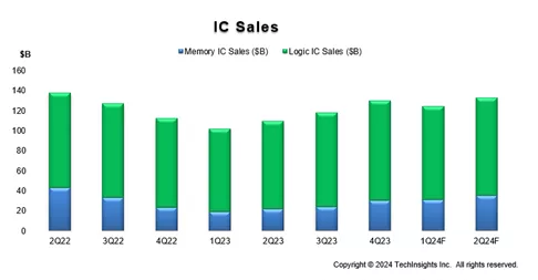
“Europe's future as a region of semiconductor manufacturing excellence is brimming with possibility,” said Laith Altimime, president of SEMI Europe. “The adoption of the European Council’s general approach marks a critical step in the passage of the European Chips Act, a landmark initiative for our industry.”

The European Parliament’s Committee on Industry, Research and Energy (ITRE) is expected to vote on the European Union Chips Act report in January 2023. The Committee will then submit the approved text to plenary for adoption, a vote scheduled for February 2023. The text would constitute the European Parliament’s negotiating position and mark the last step before the start of trialogue negotiations among the European Commission, Parliament, and Council. 

“SEMI looks forward to continued collaboration with the European institutions and our member companies to ensure the timely adoption and implementation of the European Chips Act, putting Europe’s semiconductor industry on a competitive footing with other regions,” said Christopher Frieling, director of Advocacy and Public Policy at SEMI Europe.

Visit SEMI Global Advocacy to learn more about public policy efforts and developments, and SEMI Workforce Development for more information on efforts to address the microelectronics industry’s talent needs.

For more details, contact the SEMI Europe Advocacy team:


About SEMI
SEMI® connects more than 2,500 member companies and 1.3 million professionals worldwide to advance the technology and business of electronics design and manufacturing. SEMI members are responsible for the innovations in materials, design, equipment, software, devices, and services that enable smarter, faster, more powerful, and more affordable electronic products. Electronic System Design Alliance (ESD Alliance), FlexTech, the Fab Owners Alliance (FOA), the MEMS & Sensors Industry Group (MSIG) and SOI Consortium are SEMI Strategic Technology Communities. Visit www.semi.org, contact one of our worldwide offices, and connect with SEMI on LinkedIn and Twitter to learn more.

Association Contacts

Serena Brischetto/SEMI Europe
Phone: +49 30 3030 8077-11
Email: [email protected]

Michael Hall/SEMI US
Phone: 1.408.943.7988
Email: [email protected]


BRUSSELS, Belgium ─ January 25, 2022  SEMI announced today the return of the Industry Strategy Symposium Europe (ISS Europe) 2022 as an in-person event to Brussels, Belgium, May 30, with insights from leading analysts, economists, policymakers and technologists on major forces impacting the semiconductor industry. The annual symposium offers business leaders’ perspectives on industry growth trends and intelligence to help ensure their company business plans and forecasts are based on current market conditions. Registration is now open.

ISS Europe logoThemed Resilient Europe: Semiconductors Enabling a Sustainable Digital Life, ISS Europe 2022 will examine economic, technology, market, business, and geopolitical developments and trends influencing the global electronics manufacturing industry, along with their implications for strategic business decisions. 

“2022 is a critical year for semiconductor industry leaders to seize growth opportunities for Europe by ensuring more sustainable and resilient operations,” said Laith Altimime, president of SEMI Europe. “As digital transformation accelerates, the industry is rising in importance in Europe as a force of competitive advantage, with strong implications for our future and the climate.”

ISS Europe 2022 Highlights

SESSION 1: Making Environmental Sustainability Happen

Industry leaders will explore ways for companies to focus on sustainability, increasingly embed green practices into their business models, and target disruptive innovations to reach decarbonization and other goals now being established worldwide. 

SESSION 2: Longevity of the Semiconductor Industry through Social Responsibility

Experts will take a deep dive into organizational strategies and initiatives to address the semiconductor industry’s talent crisis and make workplaces more inclusive. The session will highlight key diversity and inclusion trends impacting societies and the importance of industry role models while offering takeaways for company leaders.

SESSION 3: Strengthening Europe by Resilience in the Supply Chain

Europe is well-positioned to expand its semiconductor manufacturing industry and foster greater supply chain resilience of its microelectronics industry to help fuel EU economic growth. This session will focus on the critical need for Europe to bolster the resilience of its semiconductor industry and improve its independence.

For more details, please visit the ISS Europe 2022 website and connect with SEMI Europe on Twitter or LinkedIn – @SEMIEurope, #ISSEurope

About SEMI

SEMI® connects more than 2,400 member companies and 1.3 million professionals worldwide to advance the technology and business of electronics design and manufacturing. SEMI members are responsible for the innovations in materials, design, equipment, software, devices, and services that enable smarter, faster, more powerful, and more affordable electronic products. Electronic System Design Alliance (ESD Alliance), FlexTech, the Fab Owners Alliance (FOA), the MEMS & Sensors Industry Group (MSIG) and SOI Consortium are SEMI Strategic Technology Communities. Visit www.semi.org to learn more, contact one of our worldwide offices, and connect with SEMI on LinkedIn and Twitter.

Association Contact

Serena Brischetto / SEMI Europe
Phone: +49 30 3030 8077-11
Email: [email protected]

ROSENHEIM, Germany / KUALA LUMPUR, 5 May 2026 — esmo group (esmo), a leading global full-service systems integrator, developer, and supplier of advanced automation solutions for the semiconductor test industry, today announces the debut of its X-change Cart. A dedicated, semi-automated Device Interface Board (DIB) exchange system that enables a complete load board changeover by a single operator in under one minute, the X-change Cart addresses the safety, efficiency, and reliability challenges associated with manual board handling on the semiconductor test floor.

In high-mix semiconductor test environments, load board changeovers are a frequent and operationally significant activity. The reliance on manual handling has long presented challenges around changeover time, operator safety, and the risk of damage to high-value boards.

“Across test floors, we kept seeing the same pattern,” said Josef Weinberger, Head of Business Unit, esmo semicon. “Board changeovers were slow, physically demanding, and too dependent on individual technique. In tight spaces, that's where mistakes happen and time is lost. That observation drove us to build a dedicated solution that makes changeovers fast, repeatable, and manageable by a single operator in under a minute.”

Engineered for the Modern Test Floor

The X-change Cart removes the physical demands and variability of manual board handling from the equation entirely. Through a structured, HMI-controlled process, a single operator can lock, rotate, and transfer a board to the tester within a minute. The ability to carry two boards in a single trip makes that timescale achievable in practice. Thoughtful design details, including a ±180° rotation at the locking mechanism and a ±90° tower swivel, address the real-world constraints of a busy test floor.

Broad compatibility with leading ATE platforms (e.g. Teradyne, Advantest, SPEA and more) facilitates integration into existing multi-vendor environments without reconfiguration, allowing OSATs and IDMs to realise multiple benefits without disruption to their current setup.

For facilities with longer-term automation objectives, an optional configuration allows the interface tower to be mounted onto a customized AGV or AMR, providing a practical upgrade path toward autonomous test floor operations. The modular design further allows additional features to be incorporated as operational requirements evolve.

Weinberger added, “Reliability in production comes down to the details. The gripper head is engineered to perform consistently under real production conditions, with ESD-safe construction ensuring the board is protected at every point of contact. That level of engineering discipline is what makes the difference on a real production floor.”

X-change Cart Key Features

  • Modular DIB exchange system for reliable, error-free board loading and unloading
  • One-person operation — complete board change in under one minute
  • Transports two load boards simultaneously for rapid exchange
  • Full multi-axis rotation: ±180° at locking mechanism | ±180° Y-axis | ±90° Z-axis
  • Compatible with leading ATE platforms — Teradyne, Advantest, SPEA and more
  • Interfaces with test head, prober, DIB-loader, storage rack, and maintenance workbench
  • Tower swivels ±90° for use in narrow corridors and constrained test floor layouts
  • Integrated Human-Machine Interface (HMI), sensor detection, safety hand-brake, and modular battery
  • Optional: fully automated configuration mountable on AGV or AMR

The X-change Cart will be available for live demonstration at the esmo booth throughout SEMICON Southeast Asia 2026. Visit esmo at Booth 2145, Hall 8, Level 2, MITEC Kuala Lumpur from 5–7 May 2026, or contact [email protected] to arrange a meeting or request further information.

Gütenbach, Germany – December 16, 2025 – RENA Technologies is proud to be a key industrial partner in a new 1.3 million Euro Government-funded project led by the National Physical Laboratory (NPL) and supported by the Department for Science, Innovation and Technology (DSIT). The initiative will establish critical new metrology capabilities to strengthen the UK’s semiconductor innovation infrastructure and accelerate the development and adoption of next-generation semiconductor materials and processes.

This strategic investment underlines the UK’s commitment to maintaining global competitiveness in semiconductors, helping to attract private investment, strengthen supply chains, and support long-term economic growth. As advanced semiconductor materials become central to technologies such as electric vehicles, renewable energy, 5G communications and advanced electronics, robust measurement, verification and standards are increasingly essential.

The project brings together a broad consortium spanning industry and academia. Together, the partners cover the full innovation landscape, from materials research and process development to device fabrication and performance verification.

“At RENA, we develop advanced wet processing and surface treatment solutions that are critical in manufacturing of compound semiconductors and emerging materials. Through this collaboration, RENA will contribute industrial insight and process expertise to ensure that new measurement and testing capabilities are closely aligned with real manufacturing challenges.” States Peter Schneidewind, CEO of RENA Technologies.

While silicon remains the foundation of much of today’s semiconductor industry, many high-growth applications increasingly depend on advanced materials such as gallium arsenide (GaAs), gallium nitride (GaN), silicon carbide (SiC), and indium phosphide (InP). These materials offer superior performance in high-power, high-frequency and optoelectronic applications, but they also introduce new complexities in processing, characterization and quality assurance. Reliable standards and independent measurement methods are therefore essential to derisk innovation and support scale-up.

Through this project, consortium partners will work with NPL to:
• Develop new UK measurement and test capabilities for advanced semiconductor materials by combining academic research excellence with world-leading metrology expertise.
• Apply these capabilities to critical industry challenges, including assessing material integrity, verifying RF performance, and testing device reliability under demanding operating conditions.
• Share the resulting capabilities openly with industry, helping to build national consensus and strengthen the UK’s influence in international standards development for novel semiconductor technologies.

Following extensive consultation the consortium has identified three priority application areas where the UK can have the greatest global impact: power electronics, RF-communications, and optoelectronics. These areas align closely with RENA’s customer base and technology roadmap, particularly in power and compound semiconductor manufacturing.
By participating in this program, RENA reinforces its commitment to supporting the UK semiconductor ecosystem with industrially relevant innovation, enabling customers to adopt advanced materials with confidence, and helping position the UK as a global leader in next-generation semiconductor technologies.

About NPL
The National Physical Laboratory (NPL) is the UK's National Metrology Institute (NMI), developing and maintaining the national primary measurement standards, as well as collaborating with other NMIs to maintain the international system of measurement. As a public sector research establishment, it delivers extraordinary impact by providing the measurement capability that underpins the UK's prosperity and quality of life. NPL develops the metrology required to ensure the timely and successful deployment of new technologies and work with organizations as they develop and test new products and processes.

About RENA Technologies GmbH
RENA Technologies is a leading global supplier of production machines for wet chemical surface preparation. RENA products are used in path-breaking application fields such as semiconductors, MedTech, renewable energies, and the glass industry. RENA equipment is used to treat or modify surfaces of, for example, semiconductor wafers, solar cells, glass, optical substrates or other high-tech products using wet chemical processes. RENA offers proven standard machines as well as customer-specific solutions and process support.

OXFORD INSTRUMENTS PROVIDES COHERENT WITH STATE-OF-THE-ART, FULLY AUTOMATED PROCESSING EQUIPMENT, FOR 6” INP WAFER MANUFACTURING, ENABLING NEXT GENERATION AI APPLICATIONS

Oxford Instruments (OXIG), a leading provider of advanced plasma processing solutions for the compound semiconductor industry, announces the key role it is playing to support the industry’s first fully automated 6-inch indium phosphide (InP) wafer fabrication capability for photonic devices, led by Coherent Corp. (NYSE: COHR), a global leader in compound semiconductors and high-performance optical networking solutions.

Oxford Instruments’ cutting-edge plasma processing equipment is central to Coherent’s groundbreaking achievement of ramping up 6-inch InP fabs in Sherman, Texas, and Järfälla, Sweden. These fabs will play a pivotal role in driving advancements in AI datacentre, telecommunications, and sensing applications. Coherent’s transition to 6-inch wafers is set to deliver significant benefits, including a substantial increase in capacity, lower die cost and more than four times the number of devices per wafer.

Oxford Instruments has supplied fully automated, high-throughput 6-inch InP processing equipment, enabling Coherent to achieve these remarkable productivity gains. This advanced equipment is designed to support the transition from 800G to 1.6T products, a key requirement to meet the growing demands of AI interconnects and optical communications.

“We have been the leading supplier of InP plasma etch equipment to the datacom market, and Coherent, for many years. Our technology, with the quality, throughput and reliability that we have developed alongside excellent service, is ideally positioned to support the current device demand inflection we are seeing with the release of generative AI applications. We are delighted to be partnering with Coherent during this exciting period of market expansion and look forward to continuing to develop and release innovative and valuable plasma processing solutions.” Matt Kelly, Managing Director, Oxford Instruments Plasma Technology.

"Coherent’s move to 6-inch InP wafer fabrication marks a transformative milestone for the industry. Oxford Instruments’ expertise in plasma processing has been essential in enabling our Sherman and Järfälla fabs to reach world-class performance,” said Dr. Beck Mason, Executive Vice President – Semiconductor Devices at Coherent. “Together, we are advancing InP technology to support faster networks, greater efficiency, and the new applications that will define the future of connectivity."

The joint efforts of Oxford Instruments and Coherent have culminated in a manufacturing platform that sets the stage for the next generation of InP optoelectronic devices. These devices are critical enablers for applications ranging from AI datacentres and datacom transceivers to advanced sensing in consumer electronics and automotive technologies.