downloadGroupGroupnoun_press release_995423_000000 copyGroupnoun_Feed_96767_000000Group 19noun_pictures_1817522_000000Member company iconResource item iconStore item iconGroup 19Group 19noun_Photo_2085192_000000 Copynoun_presentation_2096081_000000Group 19Group Copy 7noun_webinar_692730_000000Path
Skip to main content
Default Banner Image

Executive

Registration

Registration for GES Taiwan 2026 is now closed.

If you have already registered, you will receive confirmation and onsite details by email ahead of the event. For questions about your registration, please contact David Chiang at [email protected].

[email protected] Executive

Travel

Venue

GES Taiwan 2026 will be held at the Junior Ballroom, 5F, Taipei Marriott Hotel, in conjunction with SEMICON Taiwan 2026.

Hotel

Taipei Marriott Hotel

GES Taiwan 2026 takes place at the Taipei Marriott Hotel, Junior Ballroom, 5F, in conjunction with SEMICON Taiwan 2026. For questions about accommodation, please contact David Chiang at [email protected].

Introduction

The Global Executive Summit (GES) convenes senior leaders from across the semiconductor value chain to drive collective progress on the industry's most pressing energy and decarbonization challenges. Following the inaugural summit in Tokyo in 2025, GES returns in 2026 as the Executive Summit on Energy and Sustainability, held in Taipei, Taiwan.

Tokyo established four priority initiatives now under active delivery: Gas Substitution, Abatement, Clean Electricity, and Fab Upstream Materials. Taiwan moves that work from alignment to execution.

This is an invitation-only event.

Day at a Glance

The summit is structured around two sessions.

Morning Session (7:45 AM – 12:30 PM) + Lunch

Diamond Sponsor:

Face-to-face GES Executive Council (GESEC) meeting to review progress and challenges on GES 2025 calls-to-action driven initiatives and to also lay out 2027 direction.  Attendance in this session is limited to current GESEC, Semiconductor Climate Consortium (SCC) and Energy Collaborative (EC) Leaders.

Afternoon Session (1:30 PM – 6:00 PM) + Happy Hour and Networking

Platinum Sponsors:



Gold Sponsors: 


This impactful session establishes the context for Taiwan's energy transition and semiconductor decarbonization. By pairing government keynotes and industry presentations with a public-private panel discussion, the session aims to surface key challenges and opportunities that can shape critical topics for inclusion in future GES Executive Council (GESEC), Semiconductor Climate Consortium (SCC) and/or Energy Collaborative (EC) initiatives. 

Taipei Marriott Hotel,
Junior Ballroom, 5F (in conjunction with SEMICON Taiwan 2026)
Zhongshan District, Taipei City
Taiwan

Open to GESEC members, SCC and EC leaders, invited executives. By invitation. Not transferable.

7:45 am - 8:15 am

Arrival and Registration

8:15 am - 8:25 am
1410-1420_Ajit_Manocha, SEMI CEO_headshot
Ajit Manocha
President & CEO
SEMI
Carolin_Seward_Google
Carolin Seward
Vice President
Google

Executive Opening Remarks

8:25 am - 8:30 am
0825-0830, Yein-Rui Hsieh, Deputy Minister, MoE_Headshot
Yein-Rui Hsieh
Deputy Minister
Ministry of Environment (MOENV)

Remarks

8:30 am - 8:45 am
Saifi Usmani, EMD Electronics
Dr. Saifi Usmani
Vice President, Sustainability
SEMI

Setting the Stage and Introduction to Agenda
8:45 am - 9:10 am
1410-1420_Lora Ho, Consultant, Corporate Sustainability Office, TSMC_Headshot
Lora Ho
Consultant, Corporate Sustainability Office
TSMC

Keynote: Building the Business Case for Sustainability

9:10 am - 9:30 am
Dan_Hutcheson_TechInsights
Dan Hutcheson
Vice Chair
TechInsights

Council Discussion: From Business Case to Action

9:30 am - 9:55 am
Bruce_Gall_Google.
Bruce Gall
Partnerships Manager
Google

Initiative Review: Gas Substitution
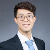
9:55 am - 10:20 am
Yong_Keong_Goh_Micron
Yong Keong Goh
Senior Manager, Environmental Sustainability
Micron
Josh_Robbins_Google
Josh Robbins
Supplier Engagement Manager, Supply Chain Sustainability
Google
Peilun headshot
Peilun Sun
Program Manager, Semiconductor Climate Consortium
SEMI

Initiative Review: Abatement

10:20 am - 10:40 am

Networking Break

10:40 am - 11:05 am
Juliana_Mora_Apple_Headshot
Juliana Mora
Program Manager, Environment & Supply Chain Innovation
Apple
Matt Morrison Headshot
Matt Morrison
Director of Sustainability
Qnity

Initiative Review: Fab Upstream Materials
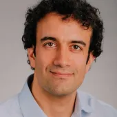
11:05 am - 11:30 am
1700 - 1745_Panel_B_Microsoft_Will Hudson_profile pic
Will Hudson
Director of Energy & Sustainability Policy, Asia-Pacific
Microsoft

Initiative Review: Clean Electricity

11:30 am - 12:10 pm
Rebecca_Green_ERM
Rebecca Green
Partner, Asia Pacific Technology Sector Lead
ERM

Council Roundtable: 2027 Direction

12:10 pm - 12:25 pm
Saifi Usmani, EMD Electronics
Dr. Saifi Usmani
Vice President, Sustainability
SEMI

Photo Call on Stage, Event Closing and Feedback Survey

All VIPs

12:25 pm - 12:30 pm
1410-1420_Ajit_Manocha, SEMI CEO_headshot
Ajit Manocha
President & CEO
SEMI
Carolin_Seward_Google
Carolin Seward
Vice President
Google

Closing Comments

12:30 pm - 1:30 pm

Networking Lunch

Open to GESEC members, SCC and EC leaders, and invited industry and government executives. By invitation.

1:30 pm - 2:00 pm

Arrival and Registration

2:00 pm - 2:10 pm
terry
Terry Tsao
Global Chief Marketing Officer and President of Taiwan
SEMI
Saifi Usmani, EMD Electronics
Dr. Saifi Usmani
Vice President, Sustainability
SEMI

Welcome Attendees and Introduction to Agenda
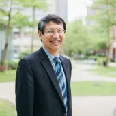
2:10 pm - 2:20 pm
1410-1420_Ajit_Manocha, SEMI CEO_headshot
Ajit Manocha
President & CEO
SEMI
1410-1420_Lora Ho, Consultant, Corporate Sustainability Office, TSMC_Headshot
Lora Ho
Consultant, Corporate Sustainability Office
TSMC
1410-1420, Tzu_Luen Lin, Deputy Executive Director, EY_headshot
Dr. Tze-Luen Alan Lin
Deputy Executive Director, Office of Energy and Carbon Reduction
Executive Yuan

Welcome Dignitaries and Official Opening of the GES

2:20 pm - 2:30 pm

Group Photo, All VIP

2:30 pm - 3:00 pm
1430-1500_Chien-Hsin Lai, Vice Minister, MoEA_Headshot
Chien-Hsin Lai
Vice Minister
Ministry of Economic Affairs

Keynote: Energy Outlook

3:00 pm - 3:25 pm
Saifi Usmani, EMD Electronics
Dr. Saifi Usmani
Vice President, Sustainability
SEMI

Keynote: GES, SCC & EC Addressing Emissions & Energy

3:25 pm - 3:45 pm

Break

3:45 pm - 4:00 pm
1545-1600_Daniel K.T. Kuo_Deputy Director, Materials Management, TSMC_Headshot
Daniel K.T. Kuo
Deputy Director, Facility Supply Chain Management Division
TSMC

Keynote: Beyond Renewable Electricity — Next Strategic Resource for Semiconductors
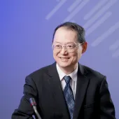
4:00 pm - 4:45 pm
1410-1420_Lora Ho, Consultant, Corporate Sustainability Office, TSMC_Headshot
Moderator: Lora Ho
Consultant, Corporate Sustainability Office
TSMC
1600-1645_Chih-Wei Wu, General Director, Energy Administration_headshot
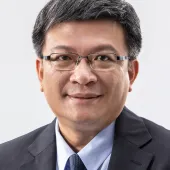
Chih-Wei Wu
Director General, Energy Administration
MoEA
1600-1645_Vincent Tseng, Chairman, Taiwan Power Company_Headshot.
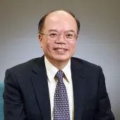
Wen-sheng Tseng
Chairman
Taiwan Power Company
1600-1645_Du Tsuen Uang, Chief Administration Officer, ASE_Headshot_0
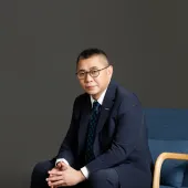
Du Tsuen Uang
Chief Administrative Officer
ASE
1600-1645_Jason Chou, General Manager, HD Renewable Energy_Headshot
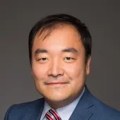
Jason Chou
General Manager
HD Renewable Energy

Panel A: Opportunities for Public-Private Partnerships in Taiwan's Energy Transition (in Mandarin with simultaneous translation to English)

4:45 pm - 5:00 pm
1645 - 1700_AMD_Justin Murrill_Profile Pic_0.
Justin Murrill
Chief Sustainability Officer
AMD

Keynote: Powering Sustainable Growth: Energy, Efficiency and Sustainability

5:00 pm - 5:45 pm
1700 - 1745_Panel_B_BNEF_Yushen Liu_
Moderator: Ms. Yushen Liu
Co-head of APAC Commercial
BloombergNEF
1700 - 1745_Panel_B_Microsoft_Will Hudson_profile pic
Will Hudson
Director of Energy & Sustainability Policy, Asia-Pacific
Microsoft
1700 - 1745_Panel_B_Google_Josh Seidenfeld
Josh Seidenfeld
Cloud Sustainability Supplier Engagement and Clean Energy Lead
Google
Han Chen_Apple_Headshot
Han Chen
Head of Clean Energy Policy for Asia
Apple
1700 - 1745_Panel_B_Brookfield_Shueh, Kai-Yuan - Corporate Photo 2
Bob Shueh
Managing Director, Energy
Brookfield Corporation

Panel B: Taiwan's Energy Transition — Key Opportunities, Challenges and Calls to Action

5:45 pm - 6:00 pm
1410-1420_Ajit_Manocha, SEMI CEO_headshot
Ajit Manocha
President & CEO
SEMI
1410-1420_Lora Ho, Consultant, Corporate Sustainability Office, TSMC_Headshot
Lora Ho
Consultant, Corporate Sustainability Office
TSMC

Closing Remarks

6:00 pm - 7:00 pm

Happy Hour and Networking

7:45 am - 7:00 pm Off Add to Calendar 2026-09-01 07:45:00 2026-09-01 19:00:00 GES Taiwan 2026: Executive Summit on Energy and Sustainability Taipei Marriott Hotel, Junior Ballroom, 5F (in conjunction with SEMICON Taiwan 2026) Zhongshan District, Taipei City Taiwan SEMI.org [email protected] Asia/Taipei public Asia/Taipei

Contact

For inquiries, please contact David Chiang at [email protected].
Event format
Tab Order
Overview
Agenda
Registration
Travel
Sponsors
Call for Abstracts
Call for Papers
Technology Showcase
Press
Photo Gallery
New Tab 1
New Tab 2
Promote in calendar
Off

SEMI Members:  $75

Use your corporate email address during log in to be recognized as a SEMI Member.

Non-Members:  $149

Students:  Free

Contact Basak Ulutas Ozturkler ([email protected]) with a picture of your student ID to receive your discount code.

United States Taiwan Belgium Germany Singapore femc30 Business Executive Technical
Highlighted content

High-temperature materials are critical for applications in harsh-environment circuitry, where devices must operate reliably under extreme thermal, chemical, and mechanical stress. In this Master Class, Dr. Shenqiang (Shen) Ren will present a high-throughput ink materials development strategy enabled by non-equilibrium processing and hybrid additive manufacturing. This approach enables rapid synthesis, combinatorial screening, and direct integration of functional materials onto diverse substrates. The resulting materials exhibit strong electrical performance, robust adhesion, and long-term stability under harsh operating conditions. This high-throughput framework accelerates the discovery and deployment of printable materials for interconnects, heaters, and EMI shielding, providing a versatile pathway toward next-generation printed electronics designed for extreme environments.

ABOUT THE SPEAKER

Shenqiang (Shen) Ren, PhD
Dr. Shenqiang Ren is a Professor of Materials Science and Engineering at the University of Maryland, College Park, with research interests in emerging functional and structural materials. He received his Ph.D. in Materials Science and Engineering from the University of Maryland, College Park, and subsequently completed postdoctoral training at the Massachusetts Institute of Technology (MIT). 

United States

Shenqiang Ren
Shenqiang (Shen) Ren , PhD
Department of Materials Science and Engineering, Professor
University of Maryland, College Park
Gity Samadi
Moderator
Gity Samadi, PhD
Sr. Director, R&D Programs
SEMI
NBMC Smart MedTech FlexTech

Join us for a focused Master Class with Dr. Shenqiang (Shen) Ren, exploring the development of high‑temperature materials for harsh‑environment printed and flexible hybrid electronics (FHE). This session will examine how devices can be engineered to operate reliably under extreme thermal, chemical, and mechanical stress—conditions where conventional materials and processes often fail.

The Master Class will also highlight how this high‑throughput framework accelerates the discovery and deployment of printable materials for interconnects, heaters, and EMI shielding, offering a versatile pathway toward next‑generation printed electronics designed for extreme conditions.

10:00 am - 12:00 pm Off Add to Calendar 2026-08-26 10:00:00 2026-08-26 12:00:00 FEMC#30 High Throughput Material Development for Extreme Environment Printed Electronics Join us for a focused Master Class with Dr. Shenqiang (Shen) Ren, exploring the development of high‑temperature materials for harsh‑environment printed and flexible hybrid electronics (FHE). This session will examine how devices can be engineered to operate reliably under extreme thermal, chemical, and mechanical stress—conditions where conventional materials and processes often fail.The Master Class will also highlight how this high‑throughput framework accelerates the discovery and deployment of printable materials for interconnects, heaters, and EMI shielding, offering a versatile pathway toward next‑generation printed electronics designed for extreme conditions. United States SEMI.org [email protected] America/Los_Angeles public America/Los_Angeles watch on-demand
Event format
Promote in calendar
Off
United States AI Techniques in Semiconductor MFG Business Executive Technical

Suggested Hotels:

Embassy Suites by Hilton Milpitas Silicon Valley

901 East Calaveras Boulevard

Milpitas, CA 95035

(408) 942-0400


Courtyard by Marriott Milpitas Silicon Valley

1480 Falcon Dr.

Milpitas, CA 95035

(408) 719-1966


Event Sponsors

Sponsorship Opportunities

Enhance your brand with our exclusive sponsorship packages. For details, contact:

Karim Somani
Email: [email protected]

Highlighted content

SEMI HQ
673 S Milpitas Blvd.
Milpitas, CA 95035
United States

Morning, Day 1: August 5th, 2026

9:00 am - 10:30 am
Surya Kalidindi
Multiscale

Emergent AI/ML Tools for Semiconductor Manufacturing Technology Optimization

Semiconductor manufacturing faces a broad set of complex challenges addressed through Yield Management Systems (YMS), Fault Detection and Classification (FDC), Run-to-Run (R2R) control, Design of Experiments (DOE), and Statistical Process Control (SPC). Existing machine learning approaches are predominantly scoped to individual process steps or short loops, leaving full-traveler analysis — essential for informed tool decisions such as hold, parameter adjustment, and recipe modification — largely unaddressed. Bespoke, step-specific models do not generalize across process nodes or design variants, and manually configuring analytical workflows for each new use case is time-intensive and error-prone as technology nodes diversify. General-purpose coding agents built on large language models (LLMs) partially close this gap by automating workflow generation, but they lack the semiconductor-specific domain knowledge required for robust, production-grade solutions: open-source ML packages carry no fab context, and proprietary data curation and signal-processing conventions are rarely captured in public training corpora.

This session shows how a fab-aware agentic approach closes that gap, focusing on three use cases: YMS, FDC, and Process DOE. It opens with a technical primer built on a common pipeline — preprocessing and feature reduction, uncertainty-aware imputation, regime-aware modeling (physics and virtual-metrology priors when data is scarce, data-driven as it grows), and interpretable attribution rather than black-box scores — instantiated differently across the three, with emphasis throughout on when a result can be trusted. YMS downselects high-dimensional metrology, imputes sparse measurements, and trains a tuned regressor ensemble (GPR, gradient-boosted trees, neural nets), with feature attribution (SHAP) mapped to process step and tool. FDC aligns traces, then layers univariate control limits (SPC) with multivariate anomaly detection (PCA, Hotelling T², MEWMA), per-sensor attribution, and alarm-budgeted limits that transfer across chambers. Process DOE designs experiments, fits uncertainty-aware surrogates (Gaussian processes), reduces dimensionality (PCA), and selects runs sequentially (single- and multi-objective Bayesian optimization). Attendees then see these techniques operationalized live by a domain-specific agentic platform and work directly with the agents on curated datasets.

By the end, attendees will understand how problem formulation, data characteristics, and method selection shape outcomes, and what distinguishes a domain-aware agentic workflow from a general-purpose coding agent. The session is interactive by design — participant choices steer the live analysis, and attendee input shapes how these capabilities evolve.

10:30 am - 11:00 am
Maryia Kurdina
AI R&D Group Leader
TEL and AI Design (TTAD)

Real-Time Equipment Health Monitoring Using Gaussian Process Regression on Sensor Signals

Will present a real-time health monitoring method for semiconductor equipment using multi-sensor time-series signals. From a small set of baseline runs (typically 5–20), Gaussian Process Regression is used to learn expected sensor behavior and associated confidence bands over repeatable operating segments. At runtime, deviations from these bands are aggregated into health scores per sensor and segment to identify abnormal behavior early. The system automatically reports anomalies and raises warnings to support proactive maintenance and reduce unplanned downtime and quality risk. To address the O(N^3) training cost of standard GPR, we use a split-training approach that achieves linear scaling, keeping computation practical for production use.​

11:00 am - 11:20 am

Break

11:20 am - 12:20 pm
Viraj Modak, Aditi Gautam, Saira Qureshi
Nvidia

Predict Before Failure: A Predictive Maintenance Blueprint with NV-Tesseract and NeMoClaw

Semiconductor fabs generate high-volume, multivariate sensor telemetry from process tools, ambient monitoring systems, sub-fab equipment, etc. Scheduling maintenance operations depends on more than just reacting to alarms/alerts: teams need to forecast how equipment will behave and detect abnormal trajectories/baseline shifts before failures occur.​

This session introduces an open Predictive Maintenance Blueprint that embeds NV-Tesseract as the core time series AI component. The pipeline performs multivariate forecasting on equipment sensor data, then runs diffusion-based anomaly detection on the forecasted window to flag emerging degradation patterns. ​

The blueprint is packaged as a reusable, deployable workflow with Hugging Face weight retrieval, configurable sensor channels, and structured outputs for downstream automation.​

We extend this blueprint with NVIDIA NeMoClaw, treating predictive maintenance as an always-on agent workflow: an autonomous agent ingests sensor streams, invokes the NV-Tesseract pipeline, interprets anomaly scores, and produces operator-ready summaries and recommended actions under OpenShell runtime guardrails. ​

Together, this shows how foundational time series models and agent orchestration can be coupled to build a production-style Predictive Maintenance stack for semiconductor operations.​

What the Audience Will Learn​:
Predictive maintenance is shifting from threshold-based SCADA alarms to forecast-then-detect workflows that catch drift earlier on multivariate equipment signatures.​

Foundational time series models (like NV-Tesseract) are increasingly deployed as components inside larger agent systems, not as standalone notebooks.​

Semiconductor and industrial teams are adopting blueprint + agent patterns (similar to NeMoClaw deployments in EDA, simulation, and factory ops) to move from prototype to governed, repeatable workflows.​

Practical lessons: multivariate sensor alignment matters; model weights and configs should be versioned and auto-retrieved; anomaly outputs must be explainable enough for maintenance engineers to trust and act on.​

Architecture takeaways:​
When to use multivariate forecasting vs. single-signal monitoring.​

Why diffusion-based anomaly detection fits correlated, high-dimensional fab sensor data better than univariate reconstruction approaches.​

How NeMoClaw can orchestrate the pipeline: data ingest → inference → thresholding → alert routing → human-in-the-loop review.

12:20 pm - 1:30 pm

Lunch

1:30 pm - 2:00 pm
Sean Tropsa & Kyle Clark
SEEQ

Practical Agentic AI at Scale for Manufacturing: Lessons Learned from Large-Scale Deployments​

Agentic AI is nearing mainstream adoption, yet many organizations still lack a clear strategy for deployments at scale. In order to bring LLM capabilities to manufacturing, companies need to go beyond what mainstream AI suppliers can deliver; they need AI deployments to be governed, reliable, repeatable, and scalable enough to earn trust and deliver measurable results. Most importantly, it must be grounded in and continuously integrate the knowledge of subject matter experts who understand the complexity of real systems and processes.​


In this session, we will share lessons learned from deploying large-scale agentic AI solutions in the semiconductor industry. We will explore how SME expertise and operational context can be embedded into Agentic AI systems to create trusted, high-value results. Specifically, we will show how an auto-Triage/RCA a Facilities Anomaly event workflow can be set up such that, as the event triggers, an AI agents completes a first pass investigation that is ready for consumption by the end user shortly after an event triggers with an optional integration with CMMS systems to ease the creation of a work order to drive faster time to resolution and greater consistency in event disposition. We will also demonstrate how engineers can build custom apps and AI agents on demand, without requiring an AI specialist or extensive coding skills, while maintaining the structure and scalability needed for enterprise adoption. Attendees will leave with practical insights for enabling better, faster decisions across engineering, technician, and operator workflows.

Afternoon, Day 1: August 5th, 2026

2:00 pm - 3:00 pm
Steven Sheets
Lam Research

Human-Machine Collaboration for Improving Semiconductor Process Development

One of the bottlenecks to building semiconductor chips is the increasing cost required to develop chemical plasma processes that form the transistors and memory storage cells1,2. These processes are still developed manually using highly trained engineers searching for a combination of tool parameters that produces an acceptable result on the silicon wafer3. The challenge for computer algorithms is the availability of limited experimental data owing to the high cost of acquisition, making it difficult to form a predictive model with accuracy to the atomic scale. Here we study Bayesian optimization algorithms to investigate how artificial intelligence (AI) might decrease the cost of developing complex semiconductor chip processes. In particular, we create a controlled virtual process game to systematically benchmark the performance of humans and computers for the design of a semiconductor fabrication process. We find that human engineers excel in the early stages of development, whereas the algorithms are far more cost-efficient near the tight tolerances of the target. Furthermore, we show that a strategy using both human designers with high expertise and algorithms in a human first–computer last strategy can reduce the cost-to-target by half compared with only human designers. Finally, we highlight cultural challenges in partnering humans with computers that need to be addressed when introducing artificial intelligence in developing semiconductor processes.​

What the Audience will Learn:
How Bayesian optimization can help enhance speed-to-solution for semiconductor manufacturing.

3:00 pm - 3:20 pm

Break

3:20 pm - 5:20 pm
Sainyam Galhotra
Third AI Automation

From Prediction to Action: Causal AI for Real-Time Root-Cause Analysis in Semiconductor Manufacturing

Semiconductor fabs generate massive volumes of data across tools, sensors, inspection systems, and process logs—yet most AI deployments remain predictive, identifying anomalies without explaining their root cause. This results in prolonged root cause analysis (RCA), costly downtime, and repeated trial-and-error fixes.​

In this talk, we present a practical approach to moving from prediction to action using causal AI. By unifying multi-modal data like images, time-series signals, and process metadata into a single intelligence layer, we enable systems that reason about cause-and-effect relationships rather than correlations.​

We will discuss how such systems can be trained efficiently using weak supervision and deployed at the edge to meet latency, privacy, and reliability requirements. We also highlight how continuous monitoring and model refinement in production ensure sustained performance in dynamic manufacturing environments.​

Drawing from real-world deployments, we show how this approach reduces RCA time from hours to minutes, improves diagnostic accuracy, and enables prescriptive actions for faster yield recovery and improved operational efficiency.​

What the Audience will Learn:​
1. Why predictive AI falls short for RCA and how causal AI bridges the gap​
2. How to build an “intelligence layer” on top of MES and traceability systems​
3. Practical methods for leveraging limited labeled data ​
4. How to integrate multi-modal data (inspection images + sensor logs + process flows)​
5. How to build AI agents that improve with more data​

How this AI technique is being used in industry today (real deployments, lessons learned, impact): In semiconductor manufacturing environments, causal AI systems are being deployed alongside existing inspection and MES infrastructure to accelerate and improve root cause analysis.​

In one deployment, defect patterns observed across multiple inspection stages were correlated with tool-level and process metadata. Instead of manual investigation across dozens of steps, the system identified a specific tool-stage interaction responsible for recurring defects. This reduced RCA time from 20–40 hours to under 10 minutes while improving diagnostic consistency.​

Demo: Yes​

Hands-on Session:
Yes,​ Applying weak supervision to label defect data with minimal manual effort​
Interpreting causal relationships across process steps​
Monitoring and updating models in a production-like setting​

5:20 pm - 7:20 pm

Reception

Morning, Day 2: August 6th, 2026

9:00 am - 10:00 am
Akhilesh Kumar​ ​
Synopsys/ANSYS

Get More from Your Sign-off Flow: Agentic AI That Makes Power & Signal Integrity Engineers Radically More Productive

Agentic AI is moving from research demos to production EDA flows, and the leverage is very clear in power and signal integrity sign-off, where engineers routinely write 1000+-API Python scripts, search for root causes through ~100 GB log files, and stitch results across half a dozen vendor tools. This talk presents our experiences with building, shipping, and supporting a multi-agent system for a production sign-off tool used on modern VLSI and 3DIC designs — covering what it took to move from a single LLM "wrapper" to a hardened agentic system that customers can actually trust with their IP.​

We will walk through the full stack: a multi-agent architecture (code-generation, log-debug, RCA/diagnostics) built on a Deep-Agent framework; an Agent Skills pattern that makes diagnostic workflows modular, composable, and customer-extensible; MCP used in both directions (the Copilot consumes vector-DB and API knowledge as MCP, and the tool itself is exposed as an MCP server so other EDA agents and customer orchestrators can drive it); and a governance layer covering tiered action approval, API-hallucination guards, prompt sanitization, audit trails, and on-premise / air-gapped local-LLM deployment. We will close on the next frontier: cross-vendor agent-to-agent flows, for example, place-and-route → parasitic extraction → power integrity → timing — orchestrated through MCP, with humans setting policy at well-defined checkpoints rather than copy-pasting between tools.​

The session is built for practitioners. A curated set of short demo videos recorded from real Agentic AI sessions on representative designs showing the agent generate scripts and run a multi-step RCA end-to-end, with explanations on what is happening under the hood at each step.​

What the Audience Will Learn​:
1. Reference architecture for a production EDA Copilot: Multi-agent decomposition (code-gen, log-debug, RCA), RAG over manuals/API catalogs, and tool execution inside the host EDA product.​
2. The Agent Skills pattern for RCA / diagnostics: Composable Agent Skills (IR-drop RCA, anomaly detection, comparative run analysis) the orchestrator plans over and that customers can extend without touching the core.​
3. MCP as a two-way integration framework: Consuming knowledge and tool capabilities as MCP and exposing the EDA tool itself as an MCP server so customer or partner agents can drive it.​
4. Governance and guardrails for production: Tiered action approval, API-validation against the catalog to block hallucinations, prompt sanitization for IP, audit trails, and runaway controls.​
5. A practical LLM strategy: Cloud frontier models, qualified open-weight local LLMs for air-gapped customers, and distillation + RL fine-tuning strategies with LLM-as-judge and production feedback.​
6. The feedback flywheel: What to instrument to drive weekly prompt fixes, monthly workflow updates, and quarterly model improvements.​
7. Cross-vendor agentic flows: Sequential chaining, parallel fan-out, and iterative loops across EDA tools over MCP.​

How This AI Technique Is Being Used in Industry Today​

The Copilot is a shipped, per-user binary that launches alongside a production sign-off tool, attaches to the user's interactive session, and runs entirely on customer infrastructure (cloud LLM or fully on-premise).​

Demo Session: Curated Videos (20 min)​

Rather than a live hands-on segment, the demo is a curated set of short, pre-recorded clips captured from real Copilot sessions on representative designs. This keeps the demonstration crisp and reproducible, and the speaker narrates each clip — calling out which agent, skill, or MCP call is firing and why.​

10:00 am - 10:20 am

Break

10:20 am - 11:20 am
Abhinav Kumar
Applied Materials

From Data Silos to Autonomous Discovery: Agentic AI in Semiconductors

Semiconductor manufacturing is increasingly challenged not by the availability of data, but by the difficulty of integrating and reasoning across fragmented, heterogeneous information sources spanning process data, metrology, and engineering knowledge. This session introduces a practical, system-level perspective on building agentic AI capabilities for semiconductor applications, beginning with foundational considerations in data definition, representation, and consistency across structured and unstructured domains.​

The discussion focuses on how these foundations enable a transition from isolated analytics toward more integrated, decision-oriented systems. Architectural patterns are explored for combining data-driven models, simulation, and domain knowledge into cohesive workflows, with emphasis on reliable orchestration, traceability of reasoning, and appropriate human oversight—elements that are critical for deploying AI in high-stakes manufacturing environments.​

The session concludes with an overview of how emerging approaches are extending these ideas toward more adaptive and semi-autonomous optimization systems. Attendees will gain a structured view of the end-to-end stack—from data preparation to decision support—and practical insights into considerations for adopting agentic AI methodologies in semiconductor manufacturing settings.

11:20 am - 11:50 am
Justin Hayes
VP of Field Engineering and Semiconductor SME
Vectara​

Building a Trustworthy Semiconductor Knowledge Base for Agentic Insight Generation

Semiconductor organizations face doubling advanced-node design costs, compressing design cycles, and scarce engineering talent while their most valuable asset, engineering knowledge, sits fragmented across schematics, waveforms, 8D reports, JIRA tickets, fab SOPs, and decades of tribal expertise. Generic search and AI tools routinely fail on this dense, technical content. ​

Drawing on real-world deployments at Broadcom, SanDisk, Altera, and Texas Instruments, Vectara will explore the solution architecture and real-world deployment of their domain-specialized Knowledge Hub and Agentic AI Platform designed specifically for the semiconductor lifecycle. ​

We'll walk through the multi-stage ingestion pipeline that preserves formulas, nested tables, and schematics natively; Vectara unified retrieval fabric that replaces fragmented, separately licensed point tools; and the agent layer that runs multi-hop, semantically deep queries across technical logs and historical failures - letting engineers surface root-cause indicators in plain language, no SQL required. ​

Crucially, the session will focus on what production-grade accuracy demands: grounded, citation-backed answers over complex IP for generating net-new insights, and streamline cross-team knowledge reuse that engineering teams, and agents can trust.

11:50 am - 1:00 pm

Lunch

Afternoon, Day 2: August 6th, 2026

1:00 pm - 2:30 pm
Garima Sharma
Mathworks

Making Sense of Equipment Time‑Series Data: From Signals to Insight

Modern semiconductor equipment generates vast amounts of time-series and inspection data, but much of it remains under-utilized. This session presents a practical, end-to-end workflow—from data preparation and AI modeling (including anomaly, defect, and drift detection) to validation and deployment—using familiar manufacturing data. It also highlights how synthetic data and generative AI can accelerate model development while maintaining robust validation and engineering control.​​

What the Audience will Learn:​
Attendees will learn how to turn equipment data into actionable insights using an end-to-end AI workflow—from data preparation to deployment. They will also see how multiple AI approaches, synthetic data, and generative AI can accelerate development while maintaining rigorous engineering validation.​

Demo / Hands-on Session: Yes

2:30 pm - 2:45 pm

Break

2:45 pm - 4:15 pm
Jon Herlocker
Cohu

Achieving Business Results from Air-gapped Agentic AI Automation in Semiconductor Manufacturing - Lessons from the Field

Agentic AI has crossed a capability line where it can now effectively automate non-trivial portions of work that previously was only done by factory engineers - process engineers, yield engineers, test engineers, maintenance engineers. At Cohu, we have been working closely every week with our customers to roll out agentic capabilities that are leading to significant automation, yield, and capacity improvements. Along the way, we have needed to overcome significant constraints - such as prohibitions on providing sensitive process data to cloud AI providers - and had to manage the more complicated issue of integrating agentic AI into legacy systems and processes. In this talk I can share some of ways that our customers are benefiting from agentic AI and talk about some of the learnings gained through these various deployments. ​

What the Audience will Learn:​
Key learnings for the audience a) real use cases of agentic AI in global semiconductor manufacturing companies; b) practical recommendations for how to prepare for and be successful with the deployment of agentic AI in semiconductor manufacturing. ​

Demo:​
FDC model creation, and fault analytics​
Yield analytics​
Tester Operations Management​
Test Engineering - lot disposition analytics ​
Maintenance optimization and predictive maintenance​
Line support optimization

- Smart MFG


The SEMI Smart Manufacturing Initiative is hosting a two-day workshop titled "AI Techniques in Semiconductor Manufacturing" at SEMI HQ in Milpitas, CA, on August 5–6, 2026. This event is part of a continuing series focused on integrating advanced AI into the semiconductor landscape. The workshop is designed to help participants understand: The real-world deployment, impact, and lessons learned from AI techniques. Strategies for building observable and scalable multi-agent workflows. The industry transition from restrictive data silos toward autonomous discovery. Methods for achieving tangible business results and automation through diverse AI applications.

8:00 am - 5:00 pm Off Add to Calendar 2026-08-05 08:00:00 2026-08-06 17:00:00 AI Techniques in Semiconductor Manufacturing  The SEMI Smart Manufacturing Initiative is hosting a two-day workshop titled "AI Techniques in Semiconductor Manufacturing" at SEMI HQ in Milpitas, CA, on August 5–6, 2026. This event is part of a continuing series focused on integrating advanced AI into the semiconductor landscape. The workshop is designed to help participants understand: The real-world deployment, impact, and lessons learned from AI techniques. Strategies for building observable and scalable multi-agent workflows. The industry transition from restrictive data silos toward autonomous discovery. Methods for achieving tangible business results and automation through diverse AI applications. SEMI HQ 673 S Milpitas Blvd. Milpitas, CA 95035 United States SEMI.org [email protected] America/Los_Angeles public America/Los_Angeles Register Now
Event format
Tab Order
Overview
Agenda
Registration
Sponsors
Travel
Promote in calendar
Off
  • SEMI Member:  $249

  • Non-Members:  $349


Cancellation Policy:

Cancellation request received on or before August 12 will be eligible for a refund. After this date, only substitutions will be accepted.  Please email your cancellation request to Agnes Cobar at [email protected]. Substitutions will only be accepted with written permission from the originally registered attendee.
For questions, please contact Pushkar Apte at [email protected]

+
United States FOC 2026 Tile Business Executive Technical

Artificial intelligence (AI) continues to grow rapidly, driving unprecedented transformation. And for all the hype, the best is yet to come! But AI's energy footprint is growing rapidly and the global “data center gold rush” is already straining energy grids and natural resources around the world. This is a formidable challenge that cannot be ignored.

For industry, this is a strategic business imperative. AI access costs are mounting, and there is increasing stakeholder pressure to show ROI on AI investments. Competitive advantage derives from running AI systems as efficiently as possible, maximizing performance and minimizing energy consumption. And for the next big application of physical AI, efficiency becomes absolutely critical.

No entity can address this alone. The SEMI Smart Data-AI Initiative has been working to build a meaningful collaboration across the entire AI ecosystem to “bend the curve.” In this workshop, together with our alliance partner San Jose, we bring together distinguished leaders across the spectrum to share insights and chart the future course. Please join us at this exciting interactive event.

Mexican Heritage Plaza
1700 Alum Rock Ave
San Jose, CA 95116
United States

Registration

8:00 am - 8:55 am

Registration, Coffee/Tea + Pastries

8:55 am - 9:00 am
pushkar apte
Pushkar Apte
Global Lead for Smart Data-AI Initiative
SEMI

Opening Remarks: Welcome

Workshop opening and introduction

9:00 am - 9:10 am
Ajit Manocha Headshot
Ajit Manocha
President & CEO
SEMI

Opening Remarks: SEMI

Overview of SEMI and Strategic Direction

9:10 am - 9:20 am
Matt Mahan, City of San Jose Mayor
Matt Mahan
Mayor
City of San Jose

Opening Remarks: Mayor Matt Mahan

9:20 am - 9:25 am
Jen Baker
Jen Baker
Director, Economic Development & Cultural Affairs
City of San Jose

Opening Remarks: City of San Jose

Innovating Together: Public-Private Sector Synergies

9:25 am - 9:45 am
Trelynd Bradley
Trelynd Bradley
Deputy Director, Innovation & Emerging Technologies
Governors Office

Keynote: State of California

From AI to Quantum, the Future is Now in California

9:45 am - 10:05 am
David Fried, Lam Research
David Fried
Chief AI Officer & Corporate VP
Lam Research

Keynote: Lam Research

From Chips to Tokens:  Efficiency and Velocity in the AI Era

10:05 am - 10:25 am
Mahmut Sinangil
Dr. Mahmut Ersin Sinangil
Distinguished Research Scientist
NVIDIA

Keynote: NVIDIA

From Watts to Intelligence: Building the Efficient AI Factory

10:25 am - 10:45 am
Yvonne Ferrier headshot
Yvonne Ferrier
Associate Principal
McKinsey & Co

Keynote: McKinsey & Co

Unlocking Efficient AI Inference at Scale

Break

10:45 am - 11:05 am

Networking Coffee Break

11:05 am - 11:10 am
Gity Samadi
Gity Samadi
Sr. Director R&D Programs
SEMI

Session Introduction: SEMI

11:10 am - 11:30 am
Vikrant Lal
Vikrant Lal
Fellow
Optical Networks Division

Session Keynote: Nokia

At the Intersection of Photonics Innovation and AI's Energy Challenge

11:30 am - 12:15 pm

Panel Discussion

Chair, Gity Samadi
• Nokia – Vikrant Lal
• Aeluma - Jonathan Klamkin, CEO
• Avicena – Nigel Alvares, VP of Product & Marketing
• Veeco – Peter Porshnev, CTO
• ASE - Speaker TBD

Networking Break

12:15 pm - 1:30 pm

Lunch

1:30 pm - 1:40 pm
Melissa
Melissa Grupen-Shemansky
VP & CTO
SEMI

Introduction to SEMI Technology Coalitions and Afternoon Sessions

1:40 pm - 2:00 pm
Christopher wellise
Christopher Wellise (CW)
VP-Sustainability
Equinix

Session Keynote: Equinix

2:00 pm - 2:10 pm
Sundeep Bajikar_Applied Materials
Sundeep Bajikar
CVP Corporate Strategy & Marketing
Applied Materials

Panel Introduction: Applied Materials

Chip-to-Grid

2:10 pm - 3:00 pm

Panel Discussion

Chair, Sundeep Bajikar
• Equinix - Christopher Wellise (CW), VP of Sustainability
• City of San Jose - Erica Garaffo, Strategic Energy Customer Development Lead
• PG&E - Karen Khamou Ornelas, Senior Director of Data Center & Technology Growth
• Deloitte Consulting - Craig Lobdell, Senior Manager, Strategy, Growth, and Transformation

Networking Break

3:00 pm - 3:20 pm

Coffee Break

3:20 pm - 3:40 pm
Nuwan Jayasena
Nuwan Jayasena
Fellow
AMD

Session Keynote: AMD

Managing Memory Architecture

3:40 pm - 4:00 pm
Cliff Young
Cliff Young
TPU & Anton Architect, MLPerf co-founder
Google

Session Keynote: Google

Bounded Revolutionary Jumps

4:00 pm - 4:45 pm

Panel Discussion

Chair, Pushkar Apte
• Google – Cliff Young
• AMD – Nuwan Jayasena
• SK Hynix – John Kim
• Siemens/Mentor – Mark Malinoski, Solutions Director, Digital Transformation Engg.
• Qualcomm - Roberto Mijat, Director for AI Product Architecture and HW Systems

4:45 pm - 5:00 pm

Wrap-up & Next Steps

5:00 pm - 6:30 pm

Reception

Smart Data & AI 8:00 am - 6:45 pm Off Add to Calendar Disabled America/Los_Angeles

Alliance Partner

City of San Jose Tile

The SEMI Smart Data-AI Initiative is organizing this workshop with our Alliance Partner, the City of San Jose. We are uniting the entire AI ecosystem including devices, materials, packaging, photonics, quantum, architectures and algorithms. Please join us in this exciting interactive workshop.

City of San Jose Tile
Register Now
Event format
Tab Order
Overview
Agenda
Registration
New Tab 1
Promote in calendar
Off
https://www.semiconindia.org/ SCI-Graphics_Reg_360x317@2_SCI_Event Tile Business Executive Expositions
Highlighted content

Yashobhoomi
Delhi
India

- APHI CAST EHS NBMC SCM Smart MFG Smart Mobility Smart MedTech Smart Data & AI SMG Sustainability EMG ESD Alliance FlexTech FOA ITL MSIG SCIS SE&A SiPAT SOI Standards Workforce Development Off Add to Calendar 2026-09-17 00:00:00 2026-09-19 00:00:00 SEMICON India 2026 Yashobhoomi Delhi India SEMI.org [email protected] America/Los_Angeles public
Event format
Promote in calendar
Off

SEMI Members:  $75

Use your corporate email address during log in to be recognized as a SEMI Member.

Non-Members:  $149

Students:  Free

Contact Basak Ulutas Ozturkler ([email protected]) with a picture of your student ID to receive your discount code.

Belgium Germany Singapore Taiwan United States FEMC31 Business Executive Technical
Highlighted content

This comprehensive course will cover the underlying fundamentals, the interrelationship between materials and processes, and the hardware used in printed electronics.  The masterclass will also explore how printed electronics can be applied currently in example applications including practical aspects of the technology, its highlights and challenges and scalability.  We will also explore emerging new technologies at the cutting edge of FHE, semiconductor packaging, photonics and quantum materials.  Throughout the course there will be opportunities for Q/A and discussions and case studies based on participant's interest.

ABOUT THE SPEAKER

J. Devin MacKenzie, PhD
Dr. Devin MacKenzie is the Washington Research Foundation Professor and an Assoc. Prof. of Materials Science and Engineering and Mechanical Engineering at UW. He is also the Technical Director of the Washington Clean Energy Testbeds, a lab that provides open-access to world-class advanced manufacturing and characterization tools for printed optoelectronics, sensors and energy device research and scale-up. Devin also has 25 years of entrepreneurial experience in sustainable materials and manufacturing of semiconductors, optoelectronics and energy devices. Prior to UW he was CEO and co-founder of printed battery company, Imprint Energy (acquired CCL/Avery), Previously, as the CTO of Add-Vision, Inc. (acquired Sumitomo Chemical), Dr. MacKenzie led R&D for roll-to-roll printed flexible OLEDs at Add-Vision with licensing in Europe and Asia. Prior to Add-Vision, he led printed silicon RF device and product engineering at Kovio, Inc. a Si Valley MIT spin-out (acquired Thin Film Electronics). Dr. MacKenzie also co-founded, Plastic Logic, from Cambridge University as a postdoc and subsequently a visiting scientist in Physics at the Cavendish Laboratory. Prior to that he worked at Bell Labs and NASA. Dr. MacKenzie has authored over 240 publications and patents that have been licensed globally and has been cited over 12,900 times in fields ranging from rare earth-doped nitrides to quantum materials. He holds Ph.D, MS, and undergraduate degrees in Materials Science and Engineering from the University of Florida and the Massachusetts Institute of Technology.

United States

J. Devin MacKenzie
J. Devin MacKenzie, PhD
Washington Research Foundation Professor of Clean Energy, Associate Professor
University of Washington
Gity Samadi
Moderator
Gity Samadi, PhD
Sr. Director, R&D Programs
SEMI
NBMC Smart MedTech FlexTech

Join us for a comprehensive Master Class with Dr. Devin MacKenzie, as he dives into the fundamentals and real-world applications of printed and flexible hybrid electronics (FHE). This session will explore the critical interrelationship between materials, processes, and hardware used in printed electronics, providing a strong foundation for understanding how these systems are designed and manufactured.

Participants will gain insight into current applications of printed electronics, along with practical considerations such as performance, scalability, and manufacturing challenges. The course will also highlight emerging technologies at the forefront of innovation, including advances in FHE, semiconductor packaging, photonics, and quantum materials

10:00 am - 12:00 pm Off Add to Calendar 2026-09-30 10:00:00 2026-09-30 12:00:00 FEMC#31 Advancing Printed Electronics Technology: From Macroelectronics to Quantum Devices Join us for a comprehensive Master Class with Dr. Devin MacKenzie, as he dives into the fundamentals and real-world applications of printed and flexible hybrid electronics (FHE). This session will explore the critical interrelationship between materials, processes, and hardware used in printed electronics, providing a strong foundation for understanding how these systems are designed and manufactured.Participants will gain insight into current applications of printed electronics, along with practical considerations such as performance, scalability, and manufacturing challenges. The course will also highlight emerging technologies at the forefront of innovation, including advances in FHE, semiconductor packaging, photonics, and quantum materials United States SEMI.org [email protected] America/Los_Angeles public America/Los_Angeles REGISTER NOW
Event format
Promote in calendar
Off
Belgium China France Germany India Ireland Italy Japan Malaysia Singapore South Korea Taiwan United States Vietnam Water Mgmt banner 350x317 Business Executive Technical

Thank you to our sponsors:  


         Sundt Construction Company & General Contractor | Sundt                                   SCREEN logo


Highlighted content

United States

9:00 am - 9:10 am

Welcome and Overview of the Water Management Working Group

9:10 am - 9:25 am
Pascal Osten
Leader, Water Solution Providers Cohort
Pascal Osten
DAS Environmental Expert GmbH

Procedures Guide

9:25 am - 9:35 am
Catherine Marsan-Loyer
Co-Lead, Fab, OSATs Cohort
Catherine Marsan-Loyer
C2MI

Water Savings Guide and Baseline-setting

9:35 am - 9:45 am
Jared Burdik
Co-Lead, Fab, OSAT Cohort
Jared Burdick
Sundt Corp.

Solutions Maturity Scale

9:45 am - 9:55 am

Q&A & WrapUp

EHS SMG Sustainability EMG FOA Standards

Join the SEMI Water Management team and document authors for a webinar discussing their research and findings for the Water Management Strategy Reports.  The reports are guides for water managers for understanding their water balance, baseline, potential savings and a general maturity scale for several solutions to be considered to move up the maturity scale to Zero Liquid Discharge (ZLD). The webinar will provide an overview on how the documents should be used to work with water solutions providers and provide strategies for both new and legacy facilities with end-of-pipe solutions as well as treatments for individual process stage water discharge. 

The webinar will include a discussion of next steps for the continued development of the reports, including how they interact with SEMI Standards and the industry roadmaps.

Reports can be downloaded HERE.

9:00 am - 10:00 am Off Add to Calendar 2026-05-21 09:00:00 2026-05-21 10:00:00 Water Management Strategies Webinar Join the SEMI Water Management team and document authors for a webinar discussing their research and findings for the Water Management Strategy Reports.  The reports are guides for water managers for understanding their water balance, baseline, potential savings and a general maturity scale for several solutions to be considered to move up the maturity scale to Zero Liquid Discharge (ZLD). The webinar will provide an overview on how the documents should be used to work with water solutions providers and provide strategies for both new and legacy facilities with end-of-pipe solutions as well as treatments for individual process stage water discharge. The webinar will include a discussion of next steps for the continued development of the reports, including how they interact with SEMI Standards and the industry roadmaps.Reports can be downloaded HERE. United States SEMI.org [email protected] America/Los_Angeles public America/Los_Angeles Watch the recorded webinar
Event format
Promote in calendar
On

Registration

Please be sure to check / understand the followings before applying

  • Due to the nature of this product, we do not accept cancellations or refunds after the application has been made. Please understand this in advance.
  • When applying for this event, please register using a corporate email address.
  • SEMI Member Price is avilable for those who work for a SEMI member company or a wholly owned subsidiary that is registered as a subsidiary. If you are unsure, please click HERE to inquire. Please note that if your membership status cannot be confirmed, you will be charged the general price.
  • Payment is only possible by credit card. You can download your receipt from Receipt / Application History in your My Page.
  • Please note that places will be allocated on a first-come, first-served basis, so please apply as soon as possible.

    First deadline: June 5 (Fri.)
    Final deadline: June 25 (Thu.)

  • Symposium Fee
    SEMI Members : 280,000 JPY (Excluding tax)
    Please note that you will be responsible for the cost of local accommodation, transportation and participation in the golf competition. 
    A shuttle bus service is scheduled to run between New Chitose Airport and the venue.
  • Accommodation Charge 
    51,460JPY - 78,660JPY per night (including Breakfast and tax)
  • Golf Competition Participation [option]
    20,000JPY (Excluding tax)
  • Other Activities [option]
    2,200JPY - 38,500JPY (Excluding tax)
  • Travel Expenses
    Please bear your own travel and transportation expenses to New Chitose Airport.

SEMI Japan Event Registration
Email: [email protected]

+
Japan Symposium Registration Accommodation and Shuttle Bus Booking Golf Registration ISS2026_top_event_bnr_508x448_en Business Executive

Accommodation and Shuttle Bus

Please see below for details on accommodations and shuttle buses.

The Windsor Hotel Toya Resort & Spa 

336 Shimizu, Toyako-cho, Abuta-gun, Hokkaido 049-5722

  • Superior Room Sea Side (40㎡) (Non-Smoking) 

    1 person usage:  51,460 JPY / night (per person) 
    2 people usage:  28,800 JPY / night (per person) 

  • Superior Room Lake Side (40㎡) (Non-smoking) 

    1 person usage:  54,760 JPY / night (per person) 
    2 people usage:  30,450 JPY / night (per person) 

  • Junior Suite Room Sea Side (58㎡) (Non-Smoking) 

    1 person usage:  72,060 JPY / night (per person) 
    2 people usage:  38,700 JPY / night (per person) 

  • Junior Suite Room Lake Side (58㎡) (Non-Smoking) 

    1 person usage:  78,660 JPY / night (per person) 
    2 people usage:  42,000 JPY / night (per person) 

    *Breakfast, consumption tax, bathing tax, and service charge are included.

[Outbound] July 8 (Wed) New Chitose Airport → Windsor Hotel Toya Resort & Spa

  • Duration: 120 minutes
  • Fare: Free (application is required)
  • Meeting / Departure: 
    Please arrive on a flight landing at New Chitose Airport between 8:30 and 10:00.
    Multiple shuttle services will be arranged to coincide with your flight arrival time.

     [For reference] Flight Schedule
    New Chitose AirportANAJAL

[Return] July 10 (Fri) The Windsor Hotel Toya Resort & Spa → New Chitose Airport

  • Travel Time: Approx. 120 minutes
  • Fare: Free (Advance reservation required)
  • Departure: 

Departures will begin from around 14:50, operating sequentially.
(Please note that departure times may vary depending on the program’s end time.)
*If you are taking the return bus, please book a flight departing at 6:30 PM or later.

JTB Global Marketing & Travel
ISS Japan 2026 Desk

*Inquiries can be received only by e-mail.
E-mail:  [email protected]
Office Hours: 10:00-16:30 (Mon-Fri except Saturdays, Sundays and Holidays)

+

Overview

We will be holding “ISS Japan 2026”, a conference to discuss strategies and issues with an eye on the future of the industry.
As digital technology supports global prosperity, we will provide opportunities for exchanging opinions and networking on important issues such as sustainability, energy issues, and the latest technology, in order for Japan to demonstrate leadership as an important base for semiconductor manufacturing.

Date
July 8 - 10, 2026
Organizer
SEMI
Supporting Organization
Hokkaido
Attendee
150
(includes Government Officials, Top Executives of Semiconductor Device, Equipment, Material, and Component Companies)

*Please note that the program is subject to change.

The Windsor Hotel TOYAResort & Spa
Shimizu, Toyako-cho, Abuta-gun
Hokkaido
049-5722
Japan

Conference Check-In, Welcome Lunch

11:15 am

Session 1 Opening

1:30 pm
Jim Hamajima
President
SEMI Japan

Opening Remarks

Ajit Manocha, SEMI
Ajit Manocha
President & CEO
SEMI

Welcome Remarks

Naomichi Suzuki
Naomichi Suzuki
Governor of Hokkaido

Guest Remarks

Daishiro-Yamagiwa
Daishiro Yamagiwa
Member, House of Representatives (LDP)
Chairman, Diet Members Caucus for the Promotion of Semiconductor Strategy(LDP)

Special Presentation

Break

2:30 pm

Session 2 Global Technology Leaders

2:40 pm
Kota Nosaka
Kota Nosaka
Representative Director, Vice President
Micron Memory Japan

Rewriting the Curve: Memory, AI, and the Next Semiconductor Era​

This talk discusses the strategic importance of next-generation memory technologies, such as DRAM and HBM, in the semiconductor industry being reshaped by rapid AI advancements. It highlights their role in boosting performance and energy efficiency, while exploring broader transformations across supply chains, industry collaboration, and talent development.

Biography

Yutaka Emoto
Yutaka Emoto
Vice President and Center General Manager
TSMC Japan 3DIC R&D Center

Advancing Tools & Materials to Empower 3DIC Manufacturing for AI Innovations

The roadmap for advanced packaging in AI applications presents significant challenges, particularly with scaling up and incorporating more chiplets.
This expansion poses obstacles in terms of yield and productivity.
To address these challenges, CoP (Chip-on-Panel) technology will be introduced to complement current CoW (Chip-on-Wafer) to accelerate 3DIC scale up. However, this shift requires substantial infrastructure development, especially for tool development and material innovations. Meanwhile, material usage will be significantly increased, raising concerns about supply chain resilience.
All of which will play a pivotal role in enabling this critical technology expansion and requires seamless collaborations across backend eco-system.

Biography

Akio Yamaguchi
Akio Yamaguchi
President and Representative Director, IBM Japan
Representative Director, Japan Association of Corporate Executives

Technological Evolution and Economic Growth

As global change accelerates and the international environment becomes increasingly uncertain, the effective use of technologies such as AI is essential for Japan to achieve sustainable economic growth. At the same time, building a “Collaborative Growth Model” rooted in empathy enables us to realize true prosperity. This lecture explores the latest technological trends and discusses Japan’s vision for sustainable growth.

Biography

Hiromichi Nozaki
Hiromichi Nozaki
National Technology Office・Chief Technology Officer
Microsoft Japan

An Autonomous Digital World Powered by AI Agents: The New Frontier of Value Creation Enabled by Generative AI

Generative AI is beginning to create an “autonomous digital world,” in which operations and decision-making are orchestrated autonomously through AI agents.
In this session, we will provide an overarching view of how these technological advancements are transforming corporate business processes, organizational structures, and executive decision-making, and examine the fundamental impact these changes have on competitiveness and business strategy.
In addition, the session will offer insights for Japanese companies and the Japanese market from a global perspective, while sharing Microsoft’s vision for the future and strategic perspectives on driving new value creation.

Biography

Break

4:40 pm

Session 3 Geopolitics, Economic Security in Asia

5:00 pm
Kazumi Nishikawa
Kazumi Nishikawa
Deputy Director General for Semiconductor and Information Policy Deputy Director General for Economic Security
Ministry of Economy, Trade and Industry

Economic Security and Semiconductor

This presentation will discuss the growing importance of the semiconductor industry amid concurrent geopolitical tensions,
supply chain disruptions, and technological advancements; outline strategies for fostering innovation and strengthening supply chain resilience;
and introduce the Japanese government’s AI and semiconductor strategy in light of these developments.

Biography

J.W. Kuo
Jyh-Huei Kuo
Former Minister of Economic Affairs, Taiwan

Inside Taiwan’s Semiconductor Strategy: Technology, Supply Chains, and Geopolitics

This presentation explores Taiwan’s semiconductor development strategy as a "pivotal fulcrum" of the global AI industry. First, it examines how Taiwan maintains its technological leadership by leveraging advanced process nodes and the unique cluster advantage of "zero distance between R&D and production". Second, from a supply chain perspective, it analyzes innovative models for the global deployment of the industrial ecosystem. Furthermore, the session addresses the strategic management of key technical know-how amidst geopolitical challenges and defines a collaborative positioning of "deep coupling" with global partners. Finally, it highlights the evolution and vision
of government policy as it transforms from a "regulator" into an "enabler".

Biography

Kazuhide Ueno
Kazuhide Ueno
Partner, Attorney-at-law
TMI Associates

Geopolitics, Economic Security, and Asia (China/India)

This session explains approaches to addressing economic security risks, incorporating the latest developments in export and investment regulations in the semiconductor sector. In particular, it focuses on risks associated with business operations in China and India.

Biography

Shuhei Yamada
Shuhei Yamada
Specially Appointed Professor, MBA Program
J. F. Oberlin University

China’s Semiconductor Supply Chain: Accelerating Self-Reliance

In March this year, the Chinese Communist Party and government adopted the 15th Five-Year Plan (2026–2030), reaffirming their commitment to accelerating “self-reliance and self-strengthening” in high-tech industries centered on semiconductors. This presentation examines how far China’s semiconductor supply chain has advanced toward greater autonomy amid prolonged U.S.–China technology tensions. By analyzing developments in key firms, it also considers how Japanese companies should respond to these changes.

Biography

Break

7:00 pm

Welcome Reception &Dinner

7:20 pm
Akira Amari
Akira Amari
Former Member of the House of Representatives
Honorary Chairman, Diet Members Caucus for the Promotion of Semiconductor Strategy(, LDP)

Kiyohiro Houkin
Kiyohiro Houkin
President
Hokkaido University

Session 4 BreakFast & Round Table

7:30 am

①Supply chain Resilience
②International Competitiveness
③Geopolitics
④Energy

Coffee Break

9:20 am

Session 5 The Insights from Round Table Discussion

9:40 am

Break

10:50 am

Session 6 Leadership and Strategy to Forge Japan's Future

11:00 am
Shingo Yamagami
Shingo Yamagami
Special Advisor
TMI Associates

How Should Japan Respond to the Turbulent World?

The world has witnessed the Russian invasion of Ukraine, China’s wolf warrior diplomacy and a series of economic coercion, and the US military operations in Venezuela as well as Iran.
How should Japan react to the measures by major powers that shake the foundations of the rules-based international order established after WWII?

Fawning China, worshipping the US, and the deterioration of Japan’s presence in the world.
How could Prime Minister Takaichi extricate Japan’s diplomacy from such a stalemate that has continued since PM Suga through PM Kishida and Ishiba?

These will be discussed candidly in light of the speaker’s 40-year-long experience as a diplomat.

Biography

Yoshimitsu Kaji
Yoshimitsu Kaji
Chairman, Chief Sustainability Development Officer
CinnamonAI

Future of Global Community, Japan and AI

As AI reshapes the world, global competition and collaboration are accelerating. How can Japan create new value and demonstrate leadership in an era with no easy answers? Drawing on perspectives from startups, global companies, local governments, and business schools, this session offers fresh insights and invites participants to rethink Japan's future in the age of AI.

Biography

Lunch

12:00 pm

Off-site Networking Activity (Option)

1:00 pm

Dinner Party

7:00 pm
Ryuichi Yokota
Ryuichi Yokota
Mayor of Chitose

Session 7 Economic and Market Trends

8:20 am
Takeru Hanaya
Takeru Hanaya
Senior Analyst, Equity Research
SMBC Nikko Securities

SPE Shaping the Next-Gen Semiconductor Industry

AI is dominating the semiconductor market. As AI-related semiconductor prices rise and demand continues to grow, the outlook for the Semiconductor Production Equipment (SPE) market is improving. In addition to demand fueled by technological innovations unique to AI semiconductors, the industry faces an urgent need to construct new fabrication facilities and add production lines to keep up with increased volumes. In this seminar, we will explore the outlook for both the semiconductor and SPE markets.

Biography

Mikiya Yamada
Mikiya Yamada
Equity Research Dept. /Senior analyst
Mizuho Securities

Semi-Materials Supporting Japan's Competitive Edge

We would like to examine the current status and future prospects of Japan's Semiconductor Materials Industries that not only provides solutions for BEOL where semiconductor elements are formed on wafer surface but also for BEOL where thermal and insulation managements are vital. We would like to briefly touch the implications of geopolitical risks.

Biography

Minami Hamanaka
Minami Hamanaka
Associate Partner
McKinsey & Company

GenAI and Chips in the Post-Training Era

AI progress continues to accelerate. Frontier development is shifting from scaling pretraining to optimizing inference and strengthening agent/orchestration layers. This drives demand beyond GPUs to DPUs and data center infrastructure. As physical AI and multimodal models rise, this talk examines the implications for the semiconductor industry.

Biography

Coffee Break

9:50 am

Session 8 Energy Security and Industrial Growth Strategies

11:00 am
Naoko Doi
Naoko Doi
Senior Research Director
The Institute of Energy Economics, Japan

Toward a Secure Electricity Supply: Meeting the AI and Semiconductor Demand

Global electricity demand is rising due to the growing needs of AI and semiconductors, alongside advancing electrification in the industry, transport, and buildings. In developing Asian countries, structural shifts toward electrification are also being pursued to counter soaring oil prices, making the securing of a stable power supply a shared global challenge.This presentation highlights future demand outlooks and proposes solutions—including AI-driven energy efficiency, grid enhancement, and "watt-bit" integration—and draws implications for Japan.

Biography

Masahiro Ueno
Masahiro Ueno
Member of the Board, Executive Vice President
Hokkaido Electric Power

Realization of GX for Hokkaido’s Growth

In light of the anticipated increase in electricity demand driven by the expansion of GX (Green Transformation) industrial development, as well as the expected growth in the adoption of renewable energy leveraging Hokkaido’s inherent potential, this presentation introduces Hokkaido Electric Power Company’s initiatives to secure power supply capacity and promote energy decarbonization toward the future industrial growth of Hokkaido.

Biography

Masahiro Kobayashi
Masahiro Kobayashi
General Manager, Business Development Department, Industry Business Division, Industrial Co-Creation Business Unit
Tokyu Land

Powering Industrial Growth with Renewable Energy

As the need for carbon neutrality becomes more urgent and AI-driven data center demand continues to grow, integrating renewable energy with industrial infrastructure is increasingly important. This session highlights our 100% renewable-powered Ishikari data center as a practical model for integrating digital and green transformation at scale.

Biography

Farewell Lunch

11:40 am

Session9 Grand Finale Japan's International Competitiveness

12:30 pm
Oliver Faynot
Olivier Faynot
Silicon Component Division Manager
CEA-Leti

Shaping the Future of High-Value-Added Electronic Products

Artificial Intelligence (AI) has push the semiconductor industry toward a great challenge of energy efficiency. AI rely on massive infrastructure that are converting electricity into token. The demand is very high at either device level (high transistor density, huge amount of memory, etc.), technology level (3D integration, 3D partitioning, etc.) and infrastructure (power management, optical interconnection, etc.). These challenges are a unique opportunity to promote innovation at system level to reach a sustainable way to support AI requirements in terms of energy.
Biography

12:30 pm
Satoshi Nohara
Satoshi Nohara
Director-General, Commerce and Information Policy Bureau
Ministry of Economy, Trade and Industry

The Future of Japan's AI and Semiconductor Strategy

This presentation examines the structural shift whereby AI and semiconductors are emerging as critical foundations that shape national competitiveness, social resilience, and economic security. It further explores the technological trajectory toward the advancement of Vertical AI and Physical AI. Against this backdrop, it highlights the importance of transforming Japan’s unique strength in real-world operational data into a new source of competitive advantage and presents a strategy for realizing a System-to-Silicon paradigm.

Biography

Jun Sawada
Jun Sawada
Chairman and Member of the Board
NTT

Toward a Science and Technology-oriented Nation: The Future of Japan

As the world grapples with challenges such as population decline and intensifying global competition, how can Japan achieve sustainable growth? This session will highlight technologies such as space, AI, and robotics from a broad perspective that spans industry, society, and philosophy. We will explore Japan’s future and strategic direction through “science and technology-oriented nation,” a concept advocated by Keidanren.
Biography

Atsuyoshi Koike
Atsuyoshi Koike
CEO
Rapidus

The Semiconductor Strategy in the Age of AI

The rise of AI is radically transforming the semiconductor industry. In this new era, the keys to success are speed and data. To thrive, we must build deep partnerships with cutting-edge global leaders while fostering strong co-creation with local communities. We will share our steps to create new innovations.

Biography

Jim Hamajima
SEMI Japan
President

Closing Remarks

End

2:40 pm

-

ISS (Industry Strategy Symposium)
Japan 2026

日本語ページはこちら

Off Add to Calendar Disabled

Off-site Networking Activity

On the afternoon of the second day, we invite you to relax and enjoy a moment of calm surrounded by the wide open skies and lush greenery of Hokkaido’s magnificent natural landscape.
As part of ISS Japan’s off-site networking activities designed to foster connections among participants, we offer not only a golf competition but also a variety of alternative activities for those who do not wish to participate in golf.

ISS Networking Golf

Golf course
Windsor Great Peak of Toya
(Adjacent to the ISS venue)

Date
Thursday, July 9

Schedule
12:00-13:00 Lunch
13:00-18:30 Golf Tournament
19:00-20:30 Dinner Party

Activities

For those not participating in the golf tournament, we invite you to enjoy a variety of activities that allow you to experience the magnificent natural landscapes of Hokkaido.
A wide range of activity programs offered by the hotel is available.
https://www.windsor-hotels.co.jp/en/activity/

Reservations can be made via the link below.
Reservation Contact Information
Tel: +81-142-73-1177 (Hours: 8:00 AM – 5:00 PM)
Email: [email protected]
* When making your reservation, please mention that you will be attending “ISS JAPAN."

 
Asia/Tokyo

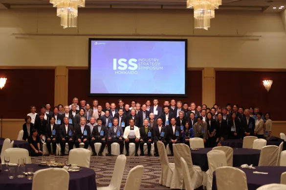
ISS Hokkaido 2025 Event Report

ISS 2025 参加者集合写真

We have compiled an overview of the 2025 event, along with photos of participants and their comments.

Download (PDF)

ISS 2025 参加者集合写真

Related blogs

ISS Europe 2025

2025-05-26

Europe’s Semiconductor Strategy: Navigating Geopolitics, Building Resilience

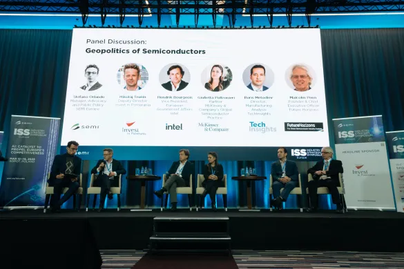
As geopolitical dynamics continue to influence global industries, the semiconductor sector finds itself at a pivotal crossroad. During the SEMI Industry Strategy Symposium (ISS Europe) held in Sopot, Poland, a high-level panel on the Geopolitics of Semiconductors brought together leaders from across the ecosystem to explore Europe’s role in an increasingly fragmented world shaped by strategic dependencies and evolving alliances.

Read More

ISS Europe 2025

Message

Event format
Tab Order
Overview
Agenda
Technology Showcase
Registration
Travel
New Tab 1
Sponsors
Promote in calendar
Off
360x317_Event_Calendar_Conductor Business Executive Technical
Highlighted content

The semiconductor industry is entering an era of deep interdependence, rapid innovation, and growing complexity. Breakthroughs in AI accelerators, advanced lithography, heterogeneous integration, and next-generation computing rely on globally distributed ecosystems of suppliers, governments, research institutions, and manufacturers. Yet intelligence systems remain fragmented, limiting visibility and slowing coordinated responses to disruptions and market shifts.

This webinar introduces Co-Intelligence™, a new model that connects intelligence across organizations—not just within them—to enable shared context, collective situational awareness, and coordinated decision-making.

We will also explore Conductor™, a platform designed to operationalize ecosystem-level intelligence by integrating signals across stakeholders and enabling faster, more aligned responses to industry challenges.

Attendees will gain:

  • A comprehensive view of Co-Intelligence™, the intelligence model for complex semiconductor ecosystems
  • Access to key insights from an industry leader 
  • An exclusive inside look at the Conductor™ platform 
  • Front-row access to the launch of a new era for the semiconductor industry and invitations to join the emerging network

Agenda:

Welcome & Introductions - Setting the Stage for Co-Intelligence™ – 5 minutes

Keynote – 10 minutes

Roundtable discussion - 10 minutes

Conductor™ Demo – 20 minutes

Q&A – 10 minutes

Session Closes – 5 minutes
 

Keynote Speaker 


I-Ting Fang
Department Manager
AI for business intelligence 
TSMC


Bio:
I-Ting Fang is a Department Manager at TSMC's Corporate Planning Organization — the “brain” for balancing demand, supply, and capacity planning. She leads teams building intelligence platforms that monitor supply chain health, assess market demand, and track potential events impacting the semiconductor industry and TSMC.

Panelists


Bettina Weiss
Chief of Staff & Corporate Strategy
SEMI


Sharon Su
Director of Strategic Supplier Partnership
Dell Technologies


Thelma Onyeka
Co-Chief Executive Officer
Beebolt


Talal Abu-Issa
Co-Chief Executive Officer
Beebolt

United States

- SCM

Semiconductor supply chain innovation and orchestration at scale now requires collective intelligence and ecosystem coordination. Join this webinar to explore Co-Intelligence™ and get an exclusive preview of the Conductor™ platform to improve visibility and resilience.

Choose your session:

  • 9-10am CST, April 9 // 6-7pm PDT, April 8 [Register Now
  • 6-7pm CST // 12-1pm CEST, April 9 [Register Now]
  • 9-10am PDT, April 10 (pre-recorded keynote with live Q&A[Register Now]
Off Add to Calendar 2026-04-08 00:00:00 2026-04-10 00:00:00 Co-Intelligence™: The New Architecture of Semiconductor Ecosystems Semiconductor supply chain innovation and orchestration at scale now requires collective intelligence and ecosystem coordination. Join this webinar to explore Co-Intelligence™ and get an exclusive preview of the Conductor™ platform to improve visibility and resilience.Choose your session:9-10am CST, April 9 // 6-7pm PDT, April 8 [Register Now] 6-7pm CST // 12-1pm CEST, April 9 [Register Now]9-10am PDT, April 10 (pre-recorded keynote with live Q&A) [Register Now] United States SEMI.org [email protected] America/Los_Angeles public America/Los_Angeles
Event format
Promote in calendar
Off