Brno, Czech Republic - July 10, 2026
Tescan, a pioneer in electron microscopy, announces the successful completion of its full acquisition by Shimadzu Corporation. As of July 7th, Tescan officially becomes a member of the Shimadzu Group, marking an important milestone in the company’s continued growth and evolution.
This step builds on the strong business alliance established in 2024 and reflects a shared commitment to advancing scientific discoveries and industrial innovations worldwide.
Strengthening the Value Delivered to Tescan Customers
“For Tescan customers, this new chapter brings enhanced capabilities, broader expertise, and expanded access to integrated solutions, while preserving the agility, innovation, and customer focus that define the Tescan way,” said Sirine Assaf, CRO, Tescan.
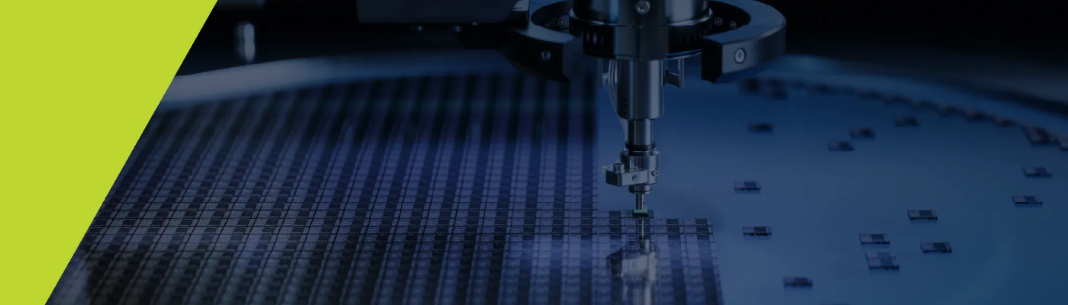
By combining Tescan’s leadership in surface analysis and electron microscopy technologies, including SEM, FIB-SEM, and TEM, with Shimadzu’s strengths in compositional and materials analysis, customers will benefit from:
More comprehensive solutions across research, development, and production workflows
Deeper application support through combined expertise in materials science, life sciences, and semiconductors
Accelerated innovation driven by joint R&D and shared technologies
Access to a larger global support network and enhanced service capabilities
Expanded product portfolio and future integrated offerings
Importantly, Tescan remains committed to maintaining its customer-centric approach, strong technical support and responsiveness, ensuring continuity in partnerships and daily operations.
Expanding Global Reach While Preserving the Tescan Way
Tescan’s growth will be further supported by Shimadzu’s global presence, particularly in Asia, alongside strengthened positions in Europe and the Americas. This will allow Tescan to:
Reach new markets and customers worldwide
Scale manufacturing and service capabilities
Enhance operational efficiency while maintaining flexibility
At the same time, Tescan will continue to operate from its headquarters in Brno, preserving its identity, expertise, and innovation culture.
Proven Track Record and Future Growth
Since its founding in 1991, Tescan has delivered over 4,000 electron microscopes across more than 80 countries, supporting customers in both research and industrial environments.
This acquisition reinforces Tescan’s long-term strategy to expand its technological leadership and deliver higher-value solutions, ensuring customers remain at the center of its development.
Continued Collaboration and Product Innovation
The successful collaboration between Tescan and Shimadzu has already been demonstrated through the joint “Shimadzu by Tescan” SEM product line introduced in Japan.
Building on this strong foundation, the integration marks a natural next step in deepening cooperation across technologies and markets. As part of this evolution, Tescan will adopt a new endorsed brand identity, “Tescan, A Shimadzu Company,” across its portfolio and communications. This reflects both the strength of the combined organizations and Tescan’s continued commitment to delivering innovative, customer-focused solutions under a globally recognized framework.
Forward-Looking Statement for Customers
This acquisition is in fully synergy with Tescan and Shimadzu strategic plans and it makrs an acceleration of what Tescan already does best: delivering high-performance systems, application-driven innovation, and close collaboration with customers.
About Tescan
Tescan develops and manufactures advanced electron microscopy solutions for materials science, life sciences, semiconductor research, industrial R&D, and quality control. With a focus on imaging performance, automation, usability, and long-term collaboration, Tescan helps researchers see the invisible and accelerate discovery through reliable, future-ready microscopy workflows.