Off
Add to Calendar2026-02-11 00:00:002026-02-13 00:00:00SEMICON Korea 2026TRANSFORM TOMORROWThe future of the semiconductor industry starts here.Join us at SEMICON Korea 2026 to shape tomorrow together. HoursFebruary 11, 2026 | 10:00-17:00 (Last entry 16:30)February 12, 2026 | 10:00-17:00 (Last entry 16:30)February 13, 2026 | 10:00-16:00 (Last entry 15:30)VenueCOEX (Hall A, B, C, D, E, Grand Ballroom, Platz and ASEM Ballroom)Westin Seoul ParnasGrand InterContinental Seoul ParnasScale550 Exhibitors, 2409 booths (2025: 501 exhibitors, 2301 booths)Seoul South KoreaSEMI.org[email protected]America/Los_Angelespublic
Early-bird Registration Close: 3 pm, Friday, May 12(KST)
Registration Fee
Early Bird (~ May 12)
SEMI Member: KRW 280,000
Non Member: KRW 330,000
On site
SEMI Member/ Student : KRW 330,000
Non Member: KRW 380,000
※ Group registration fee applies if more than 5 people are registered from one company. Please contact us by email ([email protected] ) for group registration.
Convention Hall 2, Suwon Convention Center Suwon-si Gyeonggi-do South Korea
9:00 am
-
9:05 am
Welcome
Keynote
9:05 am
-
9:35 am
Namsung Kim
Senior Director
Applied Materials
GAA(Gate-All-Around) technology to enable continuous CMOS transistor scaling for energy efficient computing solution
Namsung Kim is a Senior Director in the Integrated Module Solutions (IMS) Group at Applied Materials. He is currently responsible for managing customer engagement programs, driving business growth, and leading cross-functional teams (various Business Units) to deliver the integrated materials/modules-base product solutions across leading-edge CMOS Logic and Memory technologies. Prior to this role, he has successfully led & accomplished the definition of CMOS Logic technology roadmap, its inflections of future technology nodes and delivered multiple product development paths by validating innovative pathway solutions.
He joined Applied Materials, Inc., USA in 2015, bringing over 20 years of semiconductor device/process integration experiences (various engineering/management positions) from both CMOS Logic (GlobalFoundries/IBM alliance in USA and SSMC in Singapore) and Memory (SK-Hynix, previously LG Semi., in Korea) industries. He earned a MS in electrical and computer engineering from the National University of Singapore. He has authored and co-authored more than 50 technical publications and holds over 40 patents in the field of advanced logic (FinFETs and GAA devices) and memory technologies.
Market & Technology Trends for Memory Devices including Materials
Dr. Jeongdong Choe is a Senior Technical Fellow at TechInsights. He has over 30 years of experience in the semiconductor industry, R&D, and reverse engineering on DRAM, NAND/NOR FLASH, SRAM/Logic, and Emerging Memory. He worked for SK Hynix and Samsung Electronics for over 20 years. He joined TechInsights and has been focusing on technology analysis of semiconductor processes, materials, devices, and architecture. He has written many articles on memory technology including roadmaps, technology trends, and detailed comparisons.
Session 1: Advanced Materials for Enabling Next-Generation Devices
10:50 am
-
11:15 am
Jean-Marc Girard
CTO and Sr. VP
Air Liquide
Precursors for Memory
Jean-Marc Girard Ph.D. is CTO and Sr. VP of Manufacturing Technologies at Air Liquide Advanced Materials (ALAM), and an Air Liquid Group Fellow. He has 25 years of experience of R&D and product development management in the field of semiconductor materials and process technology in Europe, Japan and the US, and is one of the founders and was the global director of ALOHA™ from 2005 to 2010 (Air Liquide’s original CVD/ALD materials product line).
Within ALAM, Jean-Marc globally manages the Research and Development for deposition & advanced dry etching materials, oversees strategic engagements and collaborations with leading customers and equipment companies, and supervises the Intellectual Property generation and portfolio management. Since 2021, Jean-Marc’s role has expanded to leading packaging and manufacturing technology developments efforts.
11:15 am
-
11:40 am
Andy Kim
Sr. Director
Lam Research
Materials Trends in Semiconductor Manufacturing
“Byunghee Kim” has been Sr. Technologist in Lam Research since 2017.
Prior to joining Lam Research, “Kim” was director position for Samsung Electronics. During his 23 years at Samsung Electronics, “Kim” spent time doing module development, including gate, contact and BEOL.
“Kim” received a bachelor’s degree in chemistry from Yonsei Univ., Seoul, Korea and a master’s degree in MSE from Seoul Nat’l Univ., Seoul, Korea.
Jeongsik Kim, received a MS degree in Organic Synthetic Chemistry from Sogang University(Korean) in 2006 and then joined Dongjin Semichem. He had developed the patterning process materials such as bottom antireflective coating(BARC), spin on hardmask(SOH), photoresist materials in Semiconductor Materials Business Division since 2006. In 2013, he had joined the advanced lithography program of IMEC(Belgium) as Dongjin Semichem assignee and researched the ArF immersion patterning and defectivity for two years. Currently, he is in charge of developing EUV photoresist at Dongjin Semichem.
Sung Ho Kim is the Head of Specialty Gases Marketing, Clean & Etch platform, Merck KGaA, Darmstadt, Germany where he drives the execution of product marketing strategy to meet with industry’s dry etch and chamber clean gas technical and commercial needs, and leads product life cycle management and NPI (New product introduction) initiatives to help customers to advance its dry etch and chamber clean process performance. He is a proven business leader with more than 20 years of experience in the semiconductor materials industry, with a wide range of leadership experience in product marketing, product management, and technical/engineering expertise. He is based in Pangyo, Korea. Sung-Ho received a bachelor's degree in Chemical Engineering from Seoul National University.
Head of BASF Electronic Materials R&D Center in Suwon
BASF
Aiming CO2 neutrality – Sustainable Solutions for IC Applications
Won-Seob Cho, Ph.D. presently serves as the Head of the BASF Electronics Materials R&D Center in Suwon, Korea. In this esteemed position, he is responsible for leading research teams dedicated to the development of advanced wet chemical solutions, such as advanced cleaning and electroplating methods. He boasts over 20 years of research and development experience, particularly in the formulation and electrochemical screening of solutions.
Prior to joining BASF a decade ago, He served as a Principal Researcher at Samsung SDI and Samsung Fine Chemicals, where he specialized in developing planarization and electroplating solutions. Notably, his research interests have recently expanded to encompass the Advanced Package field.
Won-Seob Cho holds a distinguished Ph.D. in Chemistry from the University of Texas at Austin and has also served as a postdoctoral fellow in Supramolecular Chemistry at the University of California at Los Angeles, further solidifying his scientific expertise.
Carbon Neutral Strategy of Korean Government and Role of Material Companies
Dr. Nam, Sang Uk is conducting various studies on the ICT (semiconductor, display) industry based on economics at the KIET (Korea Institute of Industrial Research), a national research institute.
Since joining the KIET in 2018, he has participated in various studies on ICT industry policies such as Japanese export regulations, development strategy of material, parts and equipment, global value chain, and digital transformation.
In the field of carbon neutrality, he participated in major reports such as the semiconductor and display industry's carbon neutral promotion strategy and policy tasks, and the impact of RE100 on Korea's major export industries.
Materials still matter. Trends in materials demand and supply.
Mark Thirsk is Managing Partner of Linx Consulting, a leading management and strategic consulting company for electronic materials.
Mark Thirsk has experience spanning many materials and processes in wafer fabrication, combined with economic and business forecasting, strategic planning, technical marketing and M&A experience. Mark has worked in materials and equipment development, marketing, applications support, and production, as well as having expertise in business incubation, strategic development, and M&A. Mark is well placed to bring clarity and insight to market analysis from both a technical and commercial perspective. Additionally, Mark has been active in SEMI since 1999, volunteering in industry advocacy, education, and recruiting.
Mark has worked in the UK, Germany, Belgium, and the USA. Mark holds an Honours B.Sc. in Metallurgy and Materials Science from Birmingham University and an MBA
E. Jan Vardaman is president and founder of TechSearch International, Inc., which has provided market research and technology trend analysis in semiconductor packaging since 1987. She is the author of numerous publications on emerging trends in semiconductor packaging and assembly. She is a senior member of IEEE EPS and is an IEEE EPS Distinguished Lecturer. She received the IMAPS GBC Partnership award in 2012, the Daniel C. Hughes, Jr. Memorial Award in 2018, the Sidney J. Stein International Award in 2019, and she is an IMAPS Fellow. She is a member of MEPTEC, SMTA, and SEMI. Before founding TechSearch International, she served on the corporate staff of Microelectronics and Computer Technology Corporation (MCC), the electronics industry’s first pre-competitive research consortium.
Re-visioning Material Technology for Sustainable Resource Utilization and Supply Chain
Sam-Jong Choi, Ph.D. has been working as a material expert at Samsung Electronics Semiconductor for over 30 years. He joined the company in 1991 and has been responsible as a material engineer and expert for Memory Manufacturing Technology Center in Samsung Electronics by now. He obtained a Ph.D in Electronic, Computer, and Telecommunication Engineering from Hanyang University in 2020.
In 2019, he was promoted to Group Leader for Memory Material Technology Group, where he oversaw the development of new materials and quality management for Samsung Electronics. In 2020, Samjong Choi was appointed as an Corporate VP at Samsung Electronics, where he continues to play a key role in the field of semiconductor material.
As an experienced engineer and leader, he brings a wealth of knowledge and expertise to his current role, making Samsung Electronics stay at the forefront of technological innovation in the global semiconductor material industry.
In the semiconductor industry, a stable and efficient global supply chain is as important as the continuous development of advanced technology. In addition to the trade conflict and reshoring, new trends such as GWP(Global Warming Potential) are highlighted, and prompt response of the Ecosystem is essential. Accordingly, SMC Korea is trying to provide an opportunity for the semiconductor industry to discuss issues that need to be spoken out together.
SMC Korea 2023 prepares various presentations to share information on the latest technologies and markets through the participation of global leading companies while also checking global warming potential (GWP) in terms of materials. Please join us in the insights of global experts!
SMC (Strategic Materials Conference) Korea 2023
May 17(Wed), 2023 | Convention Hall 2, Suwon Convention Center
Off
Add to Calendar2023-05-17 00:00:002023-05-17 00:00:00SMC Korea 2023Semiconductor Materials for Sustainable Future
In the semiconductor industry, a stable and efficient global supply chain is as important as the continuous development of advanced technology. In addition to the trade conflict and reshoring, new trends such as GWP(Global Warming Potential) are highlighted, and prompt response of the Ecosystem is essential. Accordingly, SMC Korea is trying to provide an opportunity for the semiconductor industry to discuss issues that need to be spoken out together.
SMC Korea 2023 prepares various presentations to share information on the latest technologies and markets through the participation of global leading companies while also checking global warming potential (GWP) in terms of materials. Please join us in the insights of global experts!Convention Hall 2, Suwon Convention Center Suwon-si Gyeonggi-do South KoreaSEMI.org[email protected]Asia/Seoulpublic
Asia/Seoul
MSIG
Off
Add to Calendar2021-11-12 00:00:002021-11-12 00:00:00Smart Cities and Sensors: How to Maximize the Opportunity and What NOT to doUnited StatesSEMI.org[email protected]America/Los_Angelespublic
1
Registration Fee: $985 Members | $1,185 Non-members
Students*: $100 *Current students (18 and above) are invited to register for a student pass. Please plan to have your student ID available when picking up your badge onsite.
(Airfare and hotel accommodations are not included)
All Keynotes, tutorial, panel discussion, technical and poster sessions
All conference materials (conference proceedings, attendee list, and approved PDF presentations)
Breakfast, Lunch, and networking breaks
All Networking Events (Welcome Reception, Poster Session Reception, and Networking Happy Hour)
Complimentary entry to the Women In Semiconductors (WiS) Program ($50 value)
Complimentary registration to the SEMI Standards Meetings (Registration Required)
Discount on SEMI U Workshop registration
Discount room rate at Hilton Albany
Cancellations refund request must be submitted in writing to Taylor Zhao ([email protected]) on or before April 10, 2026 and will be subject to a $150 processing fee. After April 10, only substitution requests will be accepted.
Substitution requests are welcome and will be accepted in writing from the original registrant by May 10, 2026. Email request to Taylor Zhao ([email protected]).
If you have any questions regarding the conference or registration, please contact Taylor Zhao ([email protected]).
Align your company with the ASMC, one of the most highly respected semiconductor manufacturing conferences in the industry. The attendees are an excellent audience to expand your brand image to new and existing markets.
CONTACT
Shane Poblete Director, Sales & Business Development - Expo and Events, SEMI Tel: +1 202-847-5983 Email: [email protected]
Media Sponsors
SEMI is proud to partner with the following media to bring you news about this event. Click below to visit their website to learn more about each of them.
Advancing Semiconductor Manufacturing Excellence
ASMC is the leading international technical conference for discussing solutions that improve the collective manufacturing expertise of the semiconductor industry. Solving the challenges presented by semiconductor manufacturing is a combined effort by device makers, equipment and materials suppliers, and academics. ASMC provides an unparalleled platform for semiconductor professionals to network and learn the latest in the practical application of advanced manufacturing strategies and methodologies. Technical presentations at ASMC highlight industry innovations with specific results and select ASMC manuscripts are published in the ASMC Special Section of IEEE Transactions on Semiconductor Manufacturing.
The ASMC Committee is composed of industry professionals representing the microelectronics supply chain. All papers presented at the conference are peer-reviewed by the ASMC Technical Committee.
ASMC brings together manufacturers, equipment and materials suppliers, and academia to solve manufacturing challenges with innovative strategies and methodologies.
We are excited to partner with SEMI University on Monday, May 11 and Thursday, May 14, 2026. Whether you're a seasoned professional looking to improve your skills or a newcomer eager to break into the industry, SEMI U specializes in semiconductor training, certifications, and the technical education to support your personal and professional growth.
SEMI University (SEMI U) is the premier learning platform designed for individuals passionate about advancing their careers in the global semiconductor and electronics industry. With over 800 courses available in multiple languages and flexible formats, SEMI U empowers you with knowledge to enhance your expertise, staying ahead in our rapidly evolving field.
We look forward to reuniting with Women in Semiconductors (WiS), to be held on Thursday, May 14, 2026 at the Albany Hilton, Albany, New York.
WHO SHOULD ATTEND?
Company leaders, managers, team members, HR professionals, academia and students. Regardless of gender, we encourage attendance by everyone who is interested in fostering a more diverse, equitable and inclusive semiconductor industry, and by anyone who is responsible for developing internal or external programs to support women.
The Semiconductor Components, Instruments, and Subsystems (SCIS) Technology Community - General Meeting is on Thursday, May 14, 11:30am-1:00pm.
WHO SHOULD ATTEND?
All SEMI SCIS members are welcome to attend.
To RSVP, or if you are a SEMI member interested in learning more about how to get involved with SCIS, please contact Christie Baker at [email protected] for more information.
The Semiconductor Manufacturing Cybersecurity Consortium (SMCC) Technology Community - Hybrid General Meeting is on Wednesday, May 13, 4-5 PM. Contact [email protected] for questions and RSVP at http://tiny.cc/smcc26
Join FuzeHub in partnership with SEMI and NY Creates on May 14–15, 2026 in Albany, NY for the Glass4Chips Summit 2026.
Hosted at NY Creates (May 14) and the Hilton Albany (May 15), this two-day summit will convene leaders from industry, government, academia, and national security to:
✔ Address adoption barriers ✔ Strengthen the domestic glass supply chain ✔ Define actionable next steps to secure U.S. leadership
WHO SHOULD ATTEND?
Semiconductor manufacturers and suppliers, startups and design houses, defense stakeholders, researchers, policymakers, and ecosystem strategists.
Standards meetings are open to all, but you must be a SEMI Standards Program Member to attend.
If you are not a Member, please register for the International SEMI Standards Program and start making a big contribution to the industry’s progress, complete an application form today!
Questions? Contact your local staff coordinator: Click here
10:00 am - 11:00 am
Off
Add to Calendar2026-07-28 10:00:002026-07-28 11:00:00Traceability Japan TC Chapter MeetingTraceability Japan TC Chapter Meeting Date: Tuesday, July 28, 2026Time: 10:00 AM - 11:00 AM (JST)via Official Virtual TC Chapter Meeting + SEMI Japan (Hybrid)Please note that the meeting venue might be changed due to room capacity. If there is any change, we will inform you once it is confirmed. AGENDA Standards Contact Information:Nahoko KogaCoordinator, Standards & EHS, SEMI JapanEmail: [email protected] NOTE:Standards meetings are open to all, but you must be a SEMI Standards Program Member to attend.If you are not a Member, please register for the International SEMI Standards Program and start making a big contribution to the industry’s progress, complete an application form today! Questions? Contact your local staff coordinator: Click hereSEMI Japan 26F, xLINK Marunouchi Eiraku Bldg. 1-4-1 Marunouchi, Chiyoda-ku Chiyoda-ku, Tokyo 1000005 JapanSEMI.org[email protected]Asia/Tokyopublic
Asia/Tokyo
Standards meetings are open to all, but you must be a SEMI Standards Program Member to attend.
If you are not a Member, please register for the International SEMI Standards Program and start making a big contribution to the industry’s progress, complete an application form today!
Questions? Contact your local staff coordinator: Click here
3:00 pm - 5:00 pm
Off
Add to Calendar2026-07-10 15:00:002026-07-10 17:00:00Flexible Hybrid Electronics Japan TC Chapter MeetingFlexible Hybrid Electronics Japan TC Chapter Meeting Date: Friday, July 10, 2026Time: 3:00 PM - 5:00 PM (JST)via Official Virtual TC Chapter Meeting + SEMI Japan (Hybrid)Please note that the meeting venue might be changed due to room capacity. If there is any change, we will inform you once it is confirmed. AGENDA Standards Contact Information:Nahoko KogaCoordinator, Standards & EHS, SEMI JapanEmail: [email protected] NOTE:Standards meetings are open to all, but you must be a SEMI Standards Program Member to attend.If you are not a Member, please register for the International SEMI Standards Program and start making a big contribution to the industry’s progress, complete an application form today! Questions? Contact your local staff coordinator: Click hereSEMI Japan 26F, xLINK Marunouchi Eiraku Bldg. 1-4-1 Marunouchi, Chiyoda-ku Chiyoda-ku, Tokyo 1000005 JapanSEMI.org[email protected]Asia/Tokyopublic
Asia/Tokyo
-
Standards
8:00 am - 6:00 pm
Off
Add to Calendar2026-10-12 08:00:002026-10-15 18:00:00SEMICON West Standards Meetings 2026San Francisco, CA United StatesSEMI.org[email protected]America/Los_Angelespublic
America/Los_Angeles
High-temperature materials are critical for applications in harsh-environment circuitry, where devices must operate reliably under extreme thermal, chemical, and mechanical stress. In this Master Class, Dr. Shenqiang (Shen) Ren will present a high-throughput ink materials development strategy enabled by non-equilibrium processing and hybrid additive manufacturing. This approach enables rapid synthesis, combinatorial screening, and direct integration of functional materials onto diverse substrates. The resulting materials exhibit strong electrical performance, robust adhesion, and long-term stability under harsh operating conditions. This high-throughput framework accelerates the discovery and deployment of printable materials for interconnects, heaters, and EMI shielding, providing a versatile pathway toward next-generation printed electronics designed for extreme environments.
ABOUT THE SPEAKER
Shenqiang (Shen) Ren, PhD Dr. Shenqiang Ren is a Professor of Materials Science and Engineering at the University of Maryland, College Park, with research interests in emerging functional and structural materials. He received his Ph.D. in Materials Science and Engineering from the University of Maryland, College Park, and subsequently completed postdoctoral training at the Massachusetts Institute of Technology (MIT).
United States
Shenqiang (Shen) Ren , PhD
Department of Materials Science and Engineering, Professor
Join us for a focused Master Class with Dr. Shenqiang (Shen) Ren, exploring the development of high‑temperature materials for harsh‑environment printed and flexible hybrid electronics (FHE). This session will examine how devices can be engineered to operate reliably under extreme thermal, chemical, and mechanical stress—conditions where conventional materials and processes often fail.
The Master Class will also highlight how this high‑throughput framework accelerates the discovery and deployment of printable materials for interconnects, heaters, and EMI shielding, offering a versatile pathway toward next‑generation printed electronics designed for extreme conditions.
High Throughput Material Development for Extreme Environment Printed Electronics
Flexible Electronics Master Class #30
10:00 am - 12:00 pm
Off
Add to Calendar2026-08-26 10:00:002026-08-26 12:00:00FEMC#30 High Throughput Material Development for Extreme Environment Printed ElectronicsJoin us for a focused Master Class with Dr. Shenqiang (Shen) Ren, exploring the development of high‑temperature materials for harsh‑environment printed and flexible hybrid electronics (FHE). This session will examine how devices can be engineered to operate reliably under extreme thermal, chemical, and mechanical stress—conditions where conventional materials and processes often fail.The Master Class will also highlight how this high‑throughput framework accelerates the discovery and deployment of printable materials for interconnects, heaters, and EMI shielding, offering a versatile pathway toward next‑generation printed electronics designed for extreme conditions.United StatesSEMI.org[email protected]America/Los_Angelespublic
America/Los_Angeles
REGISTER NOW
※ Group registration fee applies to groups of five or more from the same company. ※ For group registration inquiries, please contact SEMI Korea Program Team at [email protected].
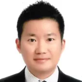
Making 3DIC Manufacturable for AI: From Vertical Integration to Scalable Production
As AI systems push requirements for higher bandwidth, lower power, and increased integration density, 3D integrated circuits (3DIC) are moving rapidly from development to production. However, scaling 3DIC introduces complex application challenges across the manufacturing flow, where process interactions and control become critical.
This talk examines key 3DIC applications and process challenges, including high aspect ratio TSV etch, void free TSV fill, and dielectric deposition, required for reliable wafer and die level stacking. Emerging applications such as inter die gap fill for advanced chiplets integration and plasma dicing for improved yield, edge quality, and die strength further increase integration complexity and productivity demands.
The presentation highlights Lam Research innovations across etch, deposition and clean processes that enable tighter process windows, improved uniformity, and higher throughput. In addition, equipment intelligence and data driven control are increasingly essential to enhance yield learning and manufacturing productivity. Together, these advances are enabling scalable, high volume 3DIC manufacturing for next generation AI systems.
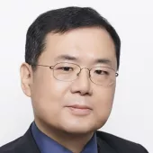
The future of compute will not be defined by silicon alone. As AI reshapes industries and economies, advanced packaging has become the foundation of the next era of innovation, enabling unprecedented gains in performance, efficiency, and scale. During his keynote, Yin Chang will explore how breakthroughs in heterogeneous integration, chiplets, and advanced manufacturing are transforming bold AI ambitions into deployable systems, and why AI leadership will depend not only on compute power, but on the ability to integrate and manufacture at scale.
The rapid electrification of automotive and industrial systems is placing increasingly stringent demands on power semiconductor devices in terms of voltage capability, thermal performance, reliability, and system integration. This presentation reviews recent trends in power devices and power module packaging technologies aimed at improving performance while addressing cost and manufacturability constraints.
First, the fundamental differences between digital and power devices are outlined, followed by an overview of power device applications based on silicon (Si), silicon carbide (SiC), and gallium nitride (GaN) technologies, together with Amkor’s product portfolio.
Next, power module packaging technologies are discussed with a focus on key electrical and thermal challenges. Representative solutions, including advanced interconnects, cooling architectures, and embedded power modules, are introduced, along with a brief overview of Amkor’s technology roadmap.
Finally, the role of the Amkor Technology Japan R&D Center in supporting open innovation and global collaboration is briefly discussed.
The presentation explores advanced packaging technologies designed to meet the escalating performance and power efficiency demands of AI and High-Performance Computing (HPC). To overcome the limitations of traditional semiconductor architectures, System Technology Co-Optimization (STCO) is introduced as a critical framework for managing thermal crosstalk and enhancing heterogeneous integration. The discussion highlights key innovations, including Customized HBM (cHBM) for optimized base-die performance and Samsung's 2.xD packaging portfolio, which encompasses Cube S, Cube E, and Cube R. Specifically, the 2.3D Cube E leverages panel level packaging to enable larger interposers and increased HBM integration, significantly improving productivity and reducing silicon fab burdens. The technical achievements in PLP—such as precise warpage control and the realization of fine RDL patterns (2/2μm)—are detailed to demonstrate their viability for large-scale AI chips. Furthermore, the roadmap extends toward 3D integration and Co-Packaged Optics (CPO) to maximize bandwidth and energy efficiency. Finally, the importance of an ecosystem-wide collaboration is emphasized as the driver for future innovation in "More than Moore" technology. These advancements collectively provide a scalable path toward the next generation of AI hardware acceleration.
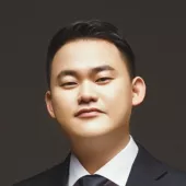
Corporate Officer, GM(General Manager) of R&D Div.
SHINKO ELECTRIC INDUSTRIES
Latest Development Status of Glass Core Build-up Substrate
Glass core substrates exhibit low CTE and significantly higher rigidity than conventional organic substrates and are therefore regarded as promising core materials for next-generation build-up packages. However, a major challenge lies in the occurrence of SeWaRe defects (delamination in glass), which arise from thermal stresses induced by the mismatch in the coefficients of thermal expansion (CTE) between the glass material and the build-up resin.
To mitigate this issue, we proposed a structure in which the corner regions of each individual piece are formed from resin. However, considering the thermal history during chip mounting, it became evident that the suppression effect was insufficient. Therefore, an edge‑protection material was applied to relieve the stress concentrated at the edges of each individual piece. As a result, it was confirmed that SeWaRe defects could be effectively suppressed even under thermal loading.
Through these efforts, we successfully developed a glass core build-up package substrate incorporating 11 layers of single‑sided copper wiring (22 layers in total).
Beyond Moore's Law: How Silicon Photonics and Advanced Packaging Are Redefining HPC
AI and data-intensive workloads are outpacing what conventional semiconductor technology can deliver. Two innovations are stepping in to close the gap: Silicon Photonics, which brings optical-speed, low-power data transmission into the data center, and Advanced Packaging, which uses chiplets and 2.5D/3D integration to maximize performance and efficiency at the chip level.
This talk examines how these complementary technologies are reshaping HPC architecture—covering their current state, how they work in tandem, and the key technical and commercial barriers to large-scale adoption.
Co-packaged optics (CPO) is emerging as a key enabler for scaling bandwidth while containing power and cost in next-generation AI and cloud infrastructure. By moving optical engines closer to the switch ASIC and shortening high-speed electrical reaches, CPO can reduce SerDes power, ease signal-integrity constraints, and increase overall front-panel bandwidth density. However, delivering these benefits at volume requires new approaches across package architecture, manufacturing, and system integration.
This presentation reviews the main packaging challenges that must be solved to industrialize CPO, including thermal management and heat spreading near high-power silicon, fiber attach and optical alignment tolerances, photonics/laser integration choices, high-density optical and electrical I/O, substrate and interposer selection, and reliability risks such as warpage, CTE mismatch, and contamination control. Test and rework strategy, yield learning, and supply-chain readiness (materials, assembly, and metrology) are highlighted as practical barriers to adoption.
The talk also outlines opportunities created by CPO packaging innovations—such as modular optical tiles, standardized fiber interfaces, advanced lid/heat-sink concepts, and co-design of electrical, mechanical, and optical domains—to unlock higher radix switches and lower system power. Attendees will leave with a structured view of technology tradeoffs, a roadmap of near-term versus long-term packaging options, and actionable considerations for bringing CPO from prototypes to deployable products.
Advanced Packaging Summit 2026, under the theme “Packaging the Future of AI – From Silicon to Photon,” will examine the evolution of packaging technologies in the AI era and their broader implications for the semiconductor industry. Featuring presentations by leading industry experts, the summit will explore market shifts driven by the growing demand for AI semiconductors, along with key technologies enabling advanced packaging. The program will also highlight the innovation journey from silicon-based integration technologies to photonics-based interconnects, which are essential to enhancing packaging productivity and scalability. Panel discussions in each session will further provide opportunities to exchange insights on real-world applications, technical challenges, and possibilities for cross-industry collaboration, while exploring new business opportunities and strategic perspectives created by advanced packaging technologies in the AI era.
ADVANCED PACKAGING SUMMIT 2026
July 15(Wed), 2026 | Convention Hall 1, 3F, Suwon Convention Center
8:30 am - 5:00 pm
Off
Add to Calendar2026-07-15 08:30:002026-07-15 17:00:00ADVANCED PACKAGING SUMMIT 2026Advanced Packaging Summit 2026, under the theme “Packaging the Future of AI – From Silicon to Photon,” will examine the evolution of packaging technologies in the AI era and their broader implications for the semiconductor industry. Featuring presentations by leading industry experts, the summit will explore market shifts driven by the growing demand for AI semiconductors, along with key technologies enabling advanced packaging. The program will also highlight the innovation journey from silicon-based integration technologies to photonics-based interconnects, which are essential to enhancing packaging productivity and scalability. Panel discussions in each session will further provide opportunities to exchange insights on real-world applications, technical challenges, and possibilities for cross-industry collaboration, while exploring new business opportunities and strategic perspectives created by advanced packaging technologies in the AI era.Convention Hall 1, 3F, Suwon Convention Center South Korea South KoreaSEMI.org[email protected]Asia/Seoulpublic
Asia/Seoul
Standards meetings are open to all, but you must be a SEMI Standards Program Member to attend.
If you are not a Member, please register for the International SEMI Standards Program and start making a big contribution to the industry’s progress, complete an application form today!
Questions? Contact your local staff coordinator: Click here
Information & Control Japan TC Chapter Meeting
10:00 am - 12:00 pm
Off
Add to Calendar2026-06-17 10:00:002026-06-17 12:00:00Information & Control Japan TC Chapter MeetingInformation & Control Japan TC Chapter Meeting Date: Wednesday, June 17, 2026Time: 10:00 am - 12:00 pm JSTVenue: SEMI Japan Office Room 1 + OVTCCM (Hybrid) AGENDA Standards Contact Information:Takeaki HirabaraStandards & EHS, SEMI JapanEmail: [email protected] NOTE:Standards meetings are open to all, but you must be a SEMI Standards Program Member to attend.If you are not a Member, please register for the International SEMI Standards Program and start making a big contribution to the industry’s progress, complete an application form today!Questions? Contact your local staff coordinator: Click here26F, xLINK Marunouchi Eiraku Bldg. 1-4-1 Marunouchi, Chiyoda-ku, Tokyo 1000005 JapanSEMI.org[email protected]Asia/Tokyopublic
Asia/Tokyo