Off
Add to Calendar2026-02-11 00:00:002026-02-13 00:00:00SEMICON Korea 2026TRANSFORM TOMORROWThe future of the semiconductor industry starts here.Join us at SEMICON Korea 2026 to shape tomorrow together. HoursFebruary 11, 2026 | 10:00-17:00 (Last entry 16:30)February 12, 2026 | 10:00-17:00 (Last entry 16:30)February 13, 2026 | 10:00-16:00 (Last entry 15:30)VenueCOEX (Hall A, B, C, D, E, Grand Ballroom, Platz and ASEM Ballroom)Westin Seoul ParnasGrand InterContinental Seoul ParnasScale550 Exhibitors, 2409 booths (2025: 501 exhibitors, 2301 booths)Seoul South KoreaSEMI.org[email protected]America/Los_Angelespublic
Early-bird Registration Close: 3 pm, Friday, May 12(KST)
Registration Fee
Early Bird (~ May 12)
SEMI Member: KRW 280,000
Non Member: KRW 330,000
On site
SEMI Member/ Student : KRW 330,000
Non Member: KRW 380,000
※ Group registration fee applies if more than 5 people are registered from one company. Please contact us by email ([email protected] ) for group registration.
Convention Hall 2, Suwon Convention Center Suwon-si Gyeonggi-do South Korea
9:00 am
-
9:05 am
Welcome
Keynote
9:05 am
-
9:35 am
Namsung Kim
Senior Director
Applied Materials
GAA(Gate-All-Around) technology to enable continuous CMOS transistor scaling for energy efficient computing solution
Namsung Kim is a Senior Director in the Integrated Module Solutions (IMS) Group at Applied Materials. He is currently responsible for managing customer engagement programs, driving business growth, and leading cross-functional teams (various Business Units) to deliver the integrated materials/modules-base product solutions across leading-edge CMOS Logic and Memory technologies. Prior to this role, he has successfully led & accomplished the definition of CMOS Logic technology roadmap, its inflections of future technology nodes and delivered multiple product development paths by validating innovative pathway solutions.
He joined Applied Materials, Inc., USA in 2015, bringing over 20 years of semiconductor device/process integration experiences (various engineering/management positions) from both CMOS Logic (GlobalFoundries/IBM alliance in USA and SSMC in Singapore) and Memory (SK-Hynix, previously LG Semi., in Korea) industries. He earned a MS in electrical and computer engineering from the National University of Singapore. He has authored and co-authored more than 50 technical publications and holds over 40 patents in the field of advanced logic (FinFETs and GAA devices) and memory technologies.
Market & Technology Trends for Memory Devices including Materials
Dr. Jeongdong Choe is a Senior Technical Fellow at TechInsights. He has over 30 years of experience in the semiconductor industry, R&D, and reverse engineering on DRAM, NAND/NOR FLASH, SRAM/Logic, and Emerging Memory. He worked for SK Hynix and Samsung Electronics for over 20 years. He joined TechInsights and has been focusing on technology analysis of semiconductor processes, materials, devices, and architecture. He has written many articles on memory technology including roadmaps, technology trends, and detailed comparisons.
Session 1: Advanced Materials for Enabling Next-Generation Devices
10:50 am
-
11:15 am
Jean-Marc Girard
CTO and Sr. VP
Air Liquide
Precursors for Memory
Jean-Marc Girard Ph.D. is CTO and Sr. VP of Manufacturing Technologies at Air Liquide Advanced Materials (ALAM), and an Air Liquid Group Fellow. He has 25 years of experience of R&D and product development management in the field of semiconductor materials and process technology in Europe, Japan and the US, and is one of the founders and was the global director of ALOHA™ from 2005 to 2010 (Air Liquide’s original CVD/ALD materials product line).
Within ALAM, Jean-Marc globally manages the Research and Development for deposition & advanced dry etching materials, oversees strategic engagements and collaborations with leading customers and equipment companies, and supervises the Intellectual Property generation and portfolio management. Since 2021, Jean-Marc’s role has expanded to leading packaging and manufacturing technology developments efforts.
11:15 am
-
11:40 am
Andy Kim
Sr. Director
Lam Research
Materials Trends in Semiconductor Manufacturing
“Byunghee Kim” has been Sr. Technologist in Lam Research since 2017.
Prior to joining Lam Research, “Kim” was director position for Samsung Electronics. During his 23 years at Samsung Electronics, “Kim” spent time doing module development, including gate, contact and BEOL.
“Kim” received a bachelor’s degree in chemistry from Yonsei Univ., Seoul, Korea and a master’s degree in MSE from Seoul Nat’l Univ., Seoul, Korea.
Jeongsik Kim, received a MS degree in Organic Synthetic Chemistry from Sogang University(Korean) in 2006 and then joined Dongjin Semichem. He had developed the patterning process materials such as bottom antireflective coating(BARC), spin on hardmask(SOH), photoresist materials in Semiconductor Materials Business Division since 2006. In 2013, he had joined the advanced lithography program of IMEC(Belgium) as Dongjin Semichem assignee and researched the ArF immersion patterning and defectivity for two years. Currently, he is in charge of developing EUV photoresist at Dongjin Semichem.
Sung Ho Kim is the Head of Specialty Gases Marketing, Clean & Etch platform, Merck KGaA, Darmstadt, Germany where he drives the execution of product marketing strategy to meet with industry’s dry etch and chamber clean gas technical and commercial needs, and leads product life cycle management and NPI (New product introduction) initiatives to help customers to advance its dry etch and chamber clean process performance. He is a proven business leader with more than 20 years of experience in the semiconductor materials industry, with a wide range of leadership experience in product marketing, product management, and technical/engineering expertise. He is based in Pangyo, Korea. Sung-Ho received a bachelor's degree in Chemical Engineering from Seoul National University.
Head of BASF Electronic Materials R&D Center in Suwon
BASF
Aiming CO2 neutrality – Sustainable Solutions for IC Applications
Won-Seob Cho, Ph.D. presently serves as the Head of the BASF Electronics Materials R&D Center in Suwon, Korea. In this esteemed position, he is responsible for leading research teams dedicated to the development of advanced wet chemical solutions, such as advanced cleaning and electroplating methods. He boasts over 20 years of research and development experience, particularly in the formulation and electrochemical screening of solutions.
Prior to joining BASF a decade ago, He served as a Principal Researcher at Samsung SDI and Samsung Fine Chemicals, where he specialized in developing planarization and electroplating solutions. Notably, his research interests have recently expanded to encompass the Advanced Package field.
Won-Seob Cho holds a distinguished Ph.D. in Chemistry from the University of Texas at Austin and has also served as a postdoctoral fellow in Supramolecular Chemistry at the University of California at Los Angeles, further solidifying his scientific expertise.
Carbon Neutral Strategy of Korean Government and Role of Material Companies
Dr. Nam, Sang Uk is conducting various studies on the ICT (semiconductor, display) industry based on economics at the KIET (Korea Institute of Industrial Research), a national research institute.
Since joining the KIET in 2018, he has participated in various studies on ICT industry policies such as Japanese export regulations, development strategy of material, parts and equipment, global value chain, and digital transformation.
In the field of carbon neutrality, he participated in major reports such as the semiconductor and display industry's carbon neutral promotion strategy and policy tasks, and the impact of RE100 on Korea's major export industries.
Materials still matter. Trends in materials demand and supply.
Mark Thirsk is Managing Partner of Linx Consulting, a leading management and strategic consulting company for electronic materials.
Mark Thirsk has experience spanning many materials and processes in wafer fabrication, combined with economic and business forecasting, strategic planning, technical marketing and M&A experience. Mark has worked in materials and equipment development, marketing, applications support, and production, as well as having expertise in business incubation, strategic development, and M&A. Mark is well placed to bring clarity and insight to market analysis from both a technical and commercial perspective. Additionally, Mark has been active in SEMI since 1999, volunteering in industry advocacy, education, and recruiting.
Mark has worked in the UK, Germany, Belgium, and the USA. Mark holds an Honours B.Sc. in Metallurgy and Materials Science from Birmingham University and an MBA
E. Jan Vardaman is president and founder of TechSearch International, Inc., which has provided market research and technology trend analysis in semiconductor packaging since 1987. She is the author of numerous publications on emerging trends in semiconductor packaging and assembly. She is a senior member of IEEE EPS and is an IEEE EPS Distinguished Lecturer. She received the IMAPS GBC Partnership award in 2012, the Daniel C. Hughes, Jr. Memorial Award in 2018, the Sidney J. Stein International Award in 2019, and she is an IMAPS Fellow. She is a member of MEPTEC, SMTA, and SEMI. Before founding TechSearch International, she served on the corporate staff of Microelectronics and Computer Technology Corporation (MCC), the electronics industry’s first pre-competitive research consortium.
Re-visioning Material Technology for Sustainable Resource Utilization and Supply Chain
Sam-Jong Choi, Ph.D. has been working as a material expert at Samsung Electronics Semiconductor for over 30 years. He joined the company in 1991 and has been responsible as a material engineer and expert for Memory Manufacturing Technology Center in Samsung Electronics by now. He obtained a Ph.D in Electronic, Computer, and Telecommunication Engineering from Hanyang University in 2020.
In 2019, he was promoted to Group Leader for Memory Material Technology Group, where he oversaw the development of new materials and quality management for Samsung Electronics. In 2020, Samjong Choi was appointed as an Corporate VP at Samsung Electronics, where he continues to play a key role in the field of semiconductor material.
As an experienced engineer and leader, he brings a wealth of knowledge and expertise to his current role, making Samsung Electronics stay at the forefront of technological innovation in the global semiconductor material industry.
In the semiconductor industry, a stable and efficient global supply chain is as important as the continuous development of advanced technology. In addition to the trade conflict and reshoring, new trends such as GWP(Global Warming Potential) are highlighted, and prompt response of the Ecosystem is essential. Accordingly, SMC Korea is trying to provide an opportunity for the semiconductor industry to discuss issues that need to be spoken out together.
SMC Korea 2023 prepares various presentations to share information on the latest technologies and markets through the participation of global leading companies while also checking global warming potential (GWP) in terms of materials. Please join us in the insights of global experts!
SMC (Strategic Materials Conference) Korea 2023
May 17(Wed), 2023 | Convention Hall 2, Suwon Convention Center
Off
Add to Calendar2023-05-17 00:00:002023-05-17 00:00:00SMC Korea 2023Semiconductor Materials for Sustainable Future
In the semiconductor industry, a stable and efficient global supply chain is as important as the continuous development of advanced technology. In addition to the trade conflict and reshoring, new trends such as GWP(Global Warming Potential) are highlighted, and prompt response of the Ecosystem is essential. Accordingly, SMC Korea is trying to provide an opportunity for the semiconductor industry to discuss issues that need to be spoken out together.
SMC Korea 2023 prepares various presentations to share information on the latest technologies and markets through the participation of global leading companies while also checking global warming potential (GWP) in terms of materials. Please join us in the insights of global experts!Convention Hall 2, Suwon Convention Center Suwon-si Gyeonggi-do South KoreaSEMI.org[email protected]Asia/Seoulpublic
Asia/Seoul
글로벌 전자산업 공급망을 대표하는 산업 협회인 SEMI의 ‘팹 전망 보고서(World Fab Forecast)’에 따르면 급격하게 증가하는 통신, 컴퓨팅, 헬스케어, 온라인 서비스, 차량용 반도체 등의 수요를 충족하기위해 올해 말까지 19개의 신규 팹이 착공되며, 2022년에는 10개의 팹이 추가로 더 착공될 것으로 보인다.
SEMI의 CEO인 아짓 마노차(Ajit Manocha)는 "세계적인 칩 부족 문제를 해결하기위해 신설될 29개 팹의 장비 투자액은 향후 몇 년간 1,400억 달러를 넘어설 것으로 예상된다.”고 말했다. 이어 그는 "중장기적으로 전 세계 팹의 생산력 확대는 자율주행차, 인공지능, 고성능 컴퓨팅, 5G~6G 통신 등 새로운 애플리케이션에 따른 반도체 수요 증가에 부응할 것"이라고 덧붙였다.
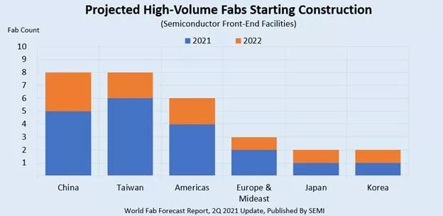
2022년까지 중국과 대만에 각각 8개, 북미 6개, 유럽 및 중동 3개, 일본과 한국에 각각 2개의 팹이(총 29개) 착공될 예정이다. 300mm 웨이퍼를 생산하는 팹은 2021년 15곳, 2022년에는 7곳이 착공에 들어간다. 나머지 7개의 팹은 100mm, 150mm, 200mm 웨이퍼를 생산하는 팹이다. 2022년까지 착공에 들어가는 팹의 전체 생산량은 월간 260만장 웨이퍼(200mm 웨이퍼 면적 기준)에 달할 것으로 전망된다.
2021년부터 2022년까지 착공되는 29개의 팹 중 15개는 파운드리 팹이며 200mm웨이퍼 기준 월간 생산량은 웨이퍼 3만에서 22만장 수준이다. 메모리 팹은 4개가 건설될 예정이며 200mm 웨이퍼 기준 월간 생산량은 10만에서 40만장 수준이다.
착공 후에 반도체 장비 설치까지는 보통 2년이 소요되기 때문에 올해 착공을 시작하는 팹 중 대다수는 2023년까지 반도체 장비 도입이 시작하지 않을 것으로 보인다. 하지만 일부 팹에는 이르면 내년 상반기부터 반도체 장비가 설치될 것으로 전망된다.
SEMI의 팹 전망 보고서에 따르면 내년에는 10개의 팹이 착공될 예정이지만 이 숫자는 칩 메이커의 결정 여부에 따라 더 증가할 수도 있다. 건설 예정인 팹의 생산량, 제품, 기술 등에 대한 자세한 내용은 SEMI 팹 전망 보고서를 통해 확인할 수 있다.
This course provides a comprehensive introduction to semiconductor manufacturing, guiding participants through the complete journey from silicon fundamentals to chip fabrication and packaging. Designed for professionals new to the semiconductor industry, the course explains key concepts, terminology, devices, and manufacturing processes used in modern fabs.
This course is divided into four modules, enabling a progressive learning experience that builds from fundamentals to manufacturing execution. Participants will gain a clear understanding of how chips are made, the role of transistors, and the steps involved in front-end manufacturing, followed by back-end assembly and packaging processes. The course also introduces the broader semiconductor ecosystem, including supply chain players, helping learners connect technical fundamentals with real-world manufacturing practices.
Who Should Attend
This course is designed for sales and marketing professionals, as well as new employees, students, and anyone interested in gaining a knowledge about semiconductor manufacturing.
Learning Objectives
Upon completion of the course, participants should be able to:
Explain fundamental semiconductor concepts, including silicon materials, doping, PN junctions, and basic device behavior.
Identify and correctly use common semiconductor manufacturing terminology.
Outline the key steps involved in front-end wafer fabrication, from bare silicon to patterned wafers.
Summarize back-end manufacturing processes, including assembly, packaging, and testing.
Topics Included
Module 1: Semiconductor Fundamentals
Introduces semiconductor basics, silicon materials, doping PN junctions, and core device concepts, building a foundation for understanding how electronic devices function.
Module 2: Semiconductor Terminologies and Manufacturing Context
Covers essential semiconductor terminology, cleanroom concepts, supply chain players, process nodes, and packaging to help learners navigate manufacturing discussions with confidence.
Module 3: Front-end and Back-end Semiconductor Manufacturing
Provides an overview of the key steps involved in front-end wafer fabrication and back-end assembly, packaging, and testing processes.
Module 4: Transistors and Their Operation
Explains different types of transistors and their working principles, showing how transistors function as switches and amplifiers inside integrated circuits.
Important Information
Note that only the person who registered will receive a certificate of completion. This virtual training will not be recorded. Attendees must be present to access the course knowledge.
Can't find the training link on the day of the training? After you register, you will receive the link to the live training via the email address you provided. In addition, you will receive email reminders 24 hours in advance and 1 hour before, with the same link. Please keep these emails on hand to access the training on time. If you do not see any confirmation emails, please check your junk/spam folders before contacting SEMI U for support.
Leverage SEMI U learning opportunities to accelerate your professional development in 2027. Our commitment remains focused on delivering comprehensive technical education that helps you build the knowledge and skills needed to thrive in the semiconductor industry.
Join us for our upcoming, "Kickstart 2027 with SEMI University," where you'll get an exclusive preview of new learning opportunities, upcoming training events, and special savings available to learners.
During this webinar, you will:
Discover the latest updates and enhancements to SEMI U's on-demand course catalog.
Explore upcoming virtual and in-person instructor-led training programs scheduled for the first half of 2027.
Learn how to maximize your professional development with SEMI U resources and learning pathways.
Receive access to a special 10% discount on all on-demand courses.
Don't miss this opportunity to plan your learning journey and stay ahead in a rapidly evolving industry. Register today to reserve your spot.
Join us to explore SEMI U's current course offerings and upcoming virtual and in-person training opportunities designed to support your professional growth in the semiconductor industry. You'll also have the chance to engage directly with our team during a live Q&A session. As a thank you for attending this free webinar, you'll receive:
A 10% discount code valid on all SEMI U on-demand courses.
Entry into a raffle to win a complimentary course bundle valued at $100.
Kickstart 2027 with SEMI University - ASIA
Webinar (PM session)
January 28, 2027
9:00 am - 9:30 am
Off
Add to Calendar2027-01-28 09:00:002027-01-28 09:30:00Kickstart 2027 with SEMI University - ASIAJoin us to explore SEMI U's current course offerings and upcoming virtual and in-person training opportunities designed to support your professional growth in the semiconductor industry. You'll also have the chance to engage directly with our team during a live Q&A session. As a thank you for attending this free webinar, you'll receive:A 10% discount code valid on all SEMI U on-demand courses. Entry into a raffle to win a complimentary course bundle valued at $100. United StatesSEMI.org[email protected]Asia/Singaporepublic
Asia/Singapore
Verific App Store Opens with Downloadable Examples of Parser Platform Applications
Verific App Store Opens with
Downloadable Examples of Parser Platform Applications
• Initial offerings include a hierarchy explorer, linter, HDL editor, signal tracer, essential tools for hardware design and verification
• Verific App Store opens July 27 as 63rd DAC begins in Long Beach, Calif.
ALAMEDA, CALIF. –– July 22, 2026 –– Verific Design Automation today announced the Verific App Store with a toolkit and downloadable example applications showcasing a variety of essential electronic design automation (EDA) point tools and solutions built using its Parser Platforms.
The Verfic App Store will open Monday, July 27, as the 63rd Design Automation Conference (DAC) convenes at the Long Beach Convention Center in Long Beach, Calif. Verific will offer in DAC Booth #1052 demonstrations of the new Verific App Store examples along with demonstrations of its SystemVerilog, Verilog, VHDL and UPF front-end Parser Platforms.
“We want to show how you can build really cool EDA products with our Platform," remarks Rob Dekker, Verific's president, founder and CTO. "In the Verific App Store, we started with a number of useful EDA point tools that are fast running, simple to license and easy to use by AI and HI (Human Intelligence) alike.”
As the leading provider of front-end platforms, Verific powers EDA with its SystemVerilog, Verilog, VHDL and UPF parser software used as the foundation for both in-house and commercially available EDA tools and flows. Applications range from synthesis and formal verification to emulation, debugging, virtual prototyping, low-power design and design-for-test tools.
Currently Available Parser Platform Apps
Example apps currently available at the Verific App Store include a hierarchy explorer, a linter, an HDL editor and a signal tracer, essential tools for hardware design and verification.
HierRTL is a Hierarchy Explorer that reports the structural hierarchy of Verilog, SystemVerilog, and VHDL designs directly from the parse tree without the need for elaboration. Engineers can visualize and navigate the hierarchical structure of their designs and understand relationships between different modules and components, making it easier to manage complex designs.
LintRTL is a Linter tool for SystemVerilog and VHDL that identifies design issues early with configurable lint rules and advanced synthesizability checks. It analyzes code for potential errors, style issues and adherence to coding standards. It helps ensure that the HDL code is clean and maintainable, reducing bugs before simulation or synthesis.
SnapRTL is an automated HDL editor used to analyze, modify and export designs while preserving the original code and formatting. It gives engineers confidence to be able to modify their designs in a specialized environment for writing and editing HDL code. SnapRTL features syntax highlighting, code completion and error detection, streamlining the coding process and improving productivity.
TraceRTL is a Signal Tracer for SystemVerilog and VHDL to improve traceability and speed debug. It monitors and analyzes signals within the design and provides insights into signal behavior during simulation, helping engineers effectively debug and optimize their designs.
Additional apps will be added in the future.
Availability and Pricing
"We will be adding more EDA point tools as we go,” says Dekker. “Currently most base products are free of charge, and we only charge a small fee for more advanced product features.”
The Verific App Store will open July 27. Tool flow developers can download the tools in the Verific Toolkit with or without being an existing Verific customer, but registration is required. New users will be asked to register with a Verific Passport account.
Basic tools are currently free, but advanced features require a monthly subscription fee. Free evaluations are available for 14 days.
Verific at DAC
Attendees can arrange demos or private meetings with Verific during DAC exhibit hours July 27-29 by sending email to [email protected].
DAC registration is open.
About Verific Design Automation
Verific Design Automation is the leading provider of SystemVerilog, Verilog, VHDL and UPF Parser Platforms that enable project groups worldwide to develop advanced electronic design automation (EDA) products quickly and cost effectively. Verific’s software serves as the front end to synthesis, formal verification, emulation, debugging, virtual prototyping, low-power design and design-for-test tools. With offices in Alameda, Calif., and Kolkata, India, Verific has shipped more than 80,000 copies of its software used by the EDA and semiconductor industry since it was founded in 1999.
Tescan Joins Shimadzu Group to Accelerate Innovation and Deliver Greater Value to Customers
Brno, Czech Republic - July 10, 2026
Tescan, a pioneer in electron microscopy, announces the successful completion of its full acquisition by Shimadzu Corporation. As of July 7th, Tescan officially becomes a member of the Shimadzu Group, marking an important milestone in the company’s continued growth and evolution.
This step builds on the strong business alliance established in 2024 and reflects a shared commitment to advancing scientific discoveries and industrial innovations worldwide.
Strengthening the Value Delivered to Tescan Customers
“For Tescan customers, this new chapter brings enhanced capabilities, broader expertise, and expanded access to integrated solutions, while preserving the agility, innovation, and customer focus that define the Tescan way,” said Sirine Assaf, CRO, Tescan.
By combining Tescan’s leadership in surface analysis and electron microscopy technologies, including SEM, FIB-SEM, and TEM, with Shimadzu’s strengths in compositional and materials analysis, customers will benefit from:
More comprehensive solutions across research, development, and production workflows
Deeper application support through combined expertise in materials science, life sciences, and semiconductors
Accelerated innovation driven by joint R&D and shared technologies
Access to a larger global support network and enhanced service capabilities
Expanded product portfolio and future integrated offerings
Importantly, Tescan remains committed to maintaining its customer-centric approach, strong technical support and responsiveness, ensuring continuity in partnerships and daily operations.
Expanding Global Reach While Preserving the Tescan Way
Tescan’s growth will be further supported by Shimadzu’s global presence, particularly in Asia, alongside strengthened positions in Europe and the Americas. This will allow Tescan to:
Reach new markets and customers worldwide
Scale manufacturing and service capabilities
Enhance operational efficiency while maintaining flexibility
At the same time, Tescan will continue to operate from its headquarters in Brno, preserving its identity, expertise, and innovation culture.
Proven Track Record and Future Growth
Since its founding in 1991, Tescan has delivered over 4,000 electron microscopes across more than 80 countries, supporting customers in both research and industrial environments.
This acquisition reinforces Tescan’s long-term strategy to expand its technological leadership and deliver higher-value solutions, ensuring customers remain at the center of its development.
Continued Collaboration and Product Innovation
The successful collaboration between Tescan and Shimadzu has already been demonstrated through the joint “Shimadzu by Tescan” SEM product line introduced in Japan.
Building on this strong foundation, the integration marks a natural next step in deepening cooperation across technologies and markets. As part of this evolution, Tescan will adopt a new endorsed brand identity, “Tescan, A Shimadzu Company,” across its portfolio and communications. This reflects both the strength of the combined organizations and Tescan’s continued commitment to delivering innovative, customer-focused solutions under a globally recognized framework.
Forward-Looking Statement for Customers
This acquisition is in fully synergy with Tescan and Shimadzu strategic plans and it makrs an acceleration of what Tescan already does best: delivering high-performance systems, application-driven innovation, and close collaboration with customers.
About Tescan
Tescan develops and manufactures advanced electron microscopy solutions for materials science, life sciences, semiconductor research, industrial R&D, and quality control. With a focus on imaging performance, automation, usability, and long-term collaboration, Tescan helps researchers see the invisible and accelerate discovery through reliable, future-ready microscopy workflows.
This course provides a comprehensive introduction to semiconductor manufacturing, guiding participants through the complete journey from silicon fundamentals to chip fabrication and packaging. Designed for professionals new to the semiconductor industry, the course explains key concepts, terminology, devices, and manufacturing processes used in modern fabs.
This course is divided into four modules, enabling a progressive learning experience that builds from fundamentals to manufacturing execution. Participants will gain a clear understanding of how chips are made, the role of transistors, and the steps involved in front-end manufacturing, followed by back-end assembly and packaging processes. The course also introduces the broader semiconductor ecosystem, including supply chain players, helping learners connect technical fundamentals with real-world manufacturing practices.
Who Should Attend
This course is designed for sales and marketing professionals, as well as new employees, students, and anyone interested in gaining a knowledge about semiconductor manufacturing.
Learning Objectives
Upon completion of the course, participants should be able to:
Explain fundamental semiconductor concepts, including silicon materials, doping, PN junctions, and basic device behavior.
Identify and correctly use common semiconductor manufacturing terminology.
Outline the key steps involved in front-end wafer fabrication, from bare silicon to patterned wafers.
Summarize back-end manufacturing processes, including assembly, packaging, and testing.
Topics Included
Module 1: Semiconductor Fundamentals
Introduces semiconductor basics, silicon materials, doping PN junctions, and core device concepts, building a foundation for understanding how electronic devices function.
Module 2: Semiconductor Terminologies and Manufacturing Context
Covers essential semiconductor terminology, cleanroom concepts, supply chain players, process nodes, and packaging to help learners navigate manufacturing discussions with confidence.
Module 3: Front-end and Back-end Semiconductor Manufacturing
Provides an overview of the key steps involved in front-end wafer fabrication and back-end assembly, packaging, and testing processes.
Module 4: Transistors and Their Operation
Explains different types of transistors and their working principles, showing how transistors function as switches and amplifiers inside integrated circuits.
Important Information
Note that only the person who registered will receive a certificate of completion. This virtual training will not be recorded. Attendees must be present to access the course knowledge.
Can't find the training link on the day of the training? After you register, you will receive the link to the live training via the email address you provided. In addition, you will receive email reminders 24 hours in advance and 1 hour before, with the same link. Please keep these emails on hand to access the training on time. If you do not see any confirmation emails, please check your junk/spam folders before contacting SEMI U for support.
Brooks Instrument Launches Ultra-Compact, High-Performance Mass Flow Controller
Brooks Instrument Launches Ultra-Compact, High-Performance Mass Flow Controller
HATFIELD, Pa. (USA), June 18, 2026 — Brooks Instrument, a world leader in precision fluid measurement and control technology, announced the global launch of its new ultra-compact AMF Series™ Advanced Mass Flow Controller. About the size of a standard Post-it® Note pad, it has the smallest footprint of any mass flow controller (MFC) in its performance class.
Combining precise gas flow control, fast response, industry-leading 1000:1 turndown capability and advanced diagnostics, the AMF Series offers equipment manufacturers and end users more operating flexibility and improved reliability and process control without the limitations of traditional compact MFCs.
“Equipment designers historically have had to choose between compact dimensions and advanced capabilities,” said Steve Kannengieszer, Global Marketing Director. “With the AMF Series, we’re changing that trade-off. Customers can now integrate high-performance flow control and predictive diagnostics into the most space-constrained systems without sacrificing accuracy, reliability or process insight.”
Advanced Features in a Compact Footprint
As equipment size across industries continues to shrink while growing in complexity and throughput, maintaining stable and precise gas flow becomes increasingly critical. The AMF Series was developed specifically to address these challenges.
With a 1-inch x 3-inch x 3-inch footprint, the MFC fits easily inside compact gas cabinets. Despite its small size, the highly accurate AMF Series features advanced capabilities, including integrated EtherNet/IP™ digital communications and onboard diagnostics for predictive maintenance.
By providing actionable diagnostic data alongside accurate flow measurement and control, the AMF Series helps users identify potential issues before they impact production, reducing unplanned downtime and improving overall equipment effectiveness.
Easier Operation and More Uptime
In addition, the AMF Series was designed to maximize uptime and simplify operation with a universal USB-C service port and embedded web-based interface that streamlines in-situ commissioning and troubleshooting. Industry-leading long-term sensor stability helps reduce maintenance requirements and eliminate periodic recipe adjustments and recalibrations.
The AMF Series also supports multi-gas configurability and simplified ordering bundles, helping OEMs reduce system complexity while streamlining product selection and integration.
Wide Range of Use
The AMF Series is especially suitable for pilot-scale applications where precise low-flow gas control and equipment miniaturization are critical, including:
• Bioprocessing and laboratory-scale bioreactors
• Thin film coating and vacuum deposition systems
• Carbon capture, utilization, and storage (CCUS)
• Hydrogen and energy transition technologies
• Analytical instrumentation
• University and research laboratories
• Industrial gas processing
Demand for Smaller Instrumentation
“Across biotechnology, we’re seeing a shift toward smaller-scale development platforms that demand greater flexibility and precision from process instrumentation,” said Joe Sipka, Business Development Director, Biotechnology. “The AMF Series was developed for micro-dosing and pilot-scale systems and delivers a wealth of digital insights—including health indicators, reliability metrics and pedigree—that enable greater automation and support a path to prescriptive maintenance. Many of these same trends are emerging in adjacent applications, such as industrial coatings, where engineers are being asked to do more with increasingly compact systems. Developed directly from conversations with our customers, the AMF Series delivers the precise low-flow control, wide operating range and reliability needed to accelerate innovation while maximizing valuable equipment space.”
About Brooks Instrument:
Since 1946, Brooks Instrument has been a leader in precision fluid measurement and control technology. Providing instrumentation for flow, pressure and vapor delivery, the company serves customers in semiconductor and high-tech manufacturing, laboratories and other processes and industries. With manufacturing, sales and service locations in the Americas, Europe and Asia, Brooks Instrument has the world’s largest installed base of mass flow controllers.
RENA Technologies Secures European Order for Advanced Cleaning Application for Specialized Semiconductor Substrates
RENA Technologies GmbH, a long-standing and experienced manufacturer of wet processing solutions for the semiconductor, advanced packaging, and solar industries, has been awarded a multi-million Euro order by a leading European semiconductor manufacturer for a specialized cleaning application designed for advanced substrates.
The solution is based on a high-performance batch wet processing platform and has been specifically engineered to deliver ultra-clean and highly efficient processing of demanding substrates. By combining advanced process control with a scalable batch architecture, the system ensures outstanding process stability, repeatability, and optimized throughput.
The customer’s decision underscores the technological strength and competitiveness of RENA’s wet processing solutions. Particularly when handling complex substrate materials, the application provides significant advantages in quality assurance, process control, and overall production efficiency. The mature cleanroom capabilities, excellent process control, and high- volume automation solutions of RENA add up to the perfect fit for the customer’s needs.
With this order, RENA further strengthens its position in the European semiconductor market and reinforces its commitment to delivering innovative, locally supported solutions to key industry players.
“Our success in securing this project highlights the growing demand for advanced wet processing technologies in Europe,” said Peter Schneidewind, CEO of RENA Technologies GmbH. “With more than 80 glass treatment tools in production worldwide - including cutting etch TGV/advanced packaging applications - RENA´s sophisticated technological solutions prove again in this new application for specialized semiconductor substrates.”