Improvement of Hybrid Bonding By Controlling Surface with Copper Pads Using Functional Water
ABSTRACT
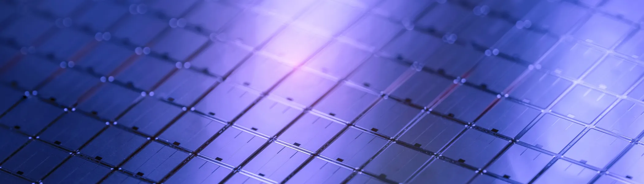
The strong demand for higher device integration density in advanced semiconductor manufacturing has driven the adoption of three-dimensional (3D) stacking technologies. Among these, wafer-to-wafer (W2W) and die-to-wafer (D2W) hybrid bonding have emerged as key enablers for next-generation packaging. Hybrid bonding, however, is inherently complex, involving copper (Cu) electrode pads on wafer surfaces where corrosion, particle adhesion, and oxidation critically influence bonding reliability. As interconnect pitch continues to scale, achieving defect-free surfaces requires highly precise post-CMP and post-dicing cleaning to remove particles and silicon debris while suppressing Cu dissolution—all under the constraint of reducing environmental impact from chemical usage.
Conventional wet processes, such as de-ionized water (DIW) rinse and traditional chemical cleaning like SC-1, face limitations in balancing particle removal efficiency with corrosion control. To address these challenges, we propose the use of functional water—ultrapure water adjusted for pH and oxidation-reduction potential with trace chemicals and gases—as a sustainable cleaning solution. To investigate the influence of rinse water on patterned wafer surfaces, various wafers were cleaned using functional waters, including hydrogen-dissolved water (DH₂W), CO₂-dissolved water (CO₂W), ultra-diluted NH₄OH (ud-NH₄OH), and ud-NH₄OH/DH₂W mixtures, prepared via a Kurita HS-13 unit.
Particle removal efficiency approached nearly 100% for particles ≥100 nm, with DH₂W combined with megasonic assistance outperforming conventional SC-1 solutions, particularly for positively charged alumina particles (Figure1). Effective removal of silicon debris post-dicing was also achieved using ud-NH4OH/DH₂W with megasonics. Mechanistically, hydrogen radicals generated during megasonic agitation in DH₂W facilitate decomposition of particle-substrate bonds, while NH₄OH enhances removal through charge repulsion under weakly alkaline conditions.
Beyond particle removal, functional water demonstrated significant advantages in corrosion prevention. While ud-NH₄OH was previously known to be effective for Cu-only systems, its performance on actual patterned wafers was unclear. The patterned wafers have complex structures, including wiring connections in lower layers and barrier metals in contact with Cu, which can trigger galvanic corrosion when exposed to water. Microscopic observations confirmed that ud-NH₄OH rinsing minimized dissolution of Cu pads (around 200 nm diameter) compared to DIW and CO2 waters (Figure2). The results obtained with DIW water were clearly inferior to those under the other conditions. The CO₂ water condition yielded better results than DIW. However, small pits were observed on the Cu pad surface treated with CO₂ water, which consequently increased the surface roughness. From these findings, it was determined that ud‑NH₄OH water exerted the most favorable influence on the Cu pad surface.
Further, statistical characterization of bonded Cu pads revealed that functional water strongly improves the surface of Cu Pads. This improvement was confirmed for state-of-the-art Cu pads with less than around 200 nm critical dimension. Overall, the ud‑NH₄OH/DH₂W process significantly improves Cu/SiCN hybrid‑bonding surfaces while reducing chemical usage, making it a strong candidate for next‑generation W2W and D2W hybrid bonding.
BIOGRAPHY

Koji Nakata is a Senior Researcher at Kurita Water Industries, with over a decade of experience in the development of water treatment technologies for semiconductor manufacturing. His work focuses on advanced wet processes, including ultrapure water systems, functional water, and chemical process optimization for front-end and advanced packaging applications.
He has been extensively involved in technology development and problem solving at semiconductor fabrication plants, addressing challenges such as particle removal, corrosion control, surface conditioning, and environmental impact reduction. His contributions include numerous patented technologies and technical presentations at international conferences related to semiconductor processing.
Through close collaboration with global device manufacturers and research institutes, he has developed a broad and practical understanding of water-related process integration in semiconductor fabs.