downloadGroupGroupnoun_press release_995423_000000 copyGroupnoun_Feed_96767_000000Group 19noun_pictures_1817522_000000Member company iconResource item iconStore item iconGroup 19Group 19noun_Photo_2085192_000000 Copynoun_presentation_2096081_000000Group 19Group Copy 7noun_webinar_692730_000000Path
Skip to main content
Default Banner Image

United States

REGISTRATION

Attendance is free, but registration is required by March 10, 2025.

United States PDS Generic Thumbnail 690x448x

SEMI Professional Development Seminar—Connecting College Students to the Semiconductor Industry 

Learn about career opportunities in high tech and acquire valuable, practical information that will help you choose career directions and plan for your success.

Come learn about careers in the semiconductor industry at the SEMI Professional Development Seminar hosted by Missouri S&T.

  • Listen to professionals in the industry talk about their roles and find out how to prepare for jobs in the Semiconductors Industry. 
  • Discover semiconductor job opportunities you didn't know existed (internship and entry-level) and how you can prepare for them through job searches, interviews, resumes, and more.
  • Meet with professionals and executives during our speed mentoring, mock interview, and networking sessions.

All majors are welcome! Students with a background in Engineering, Computer Science, Chemistry, Physics, Math, Data Science, and Business are strongly encouraged to attend.

  • Enjoy free food, free swag, and giveaways.
  • Students can come and go.

EVENT is FREE but registration is required. Registration deadline coming soon! 

Missouri University of Science and Technology
MO
United States

MONDAY, MARCH 17, 2025 (Times in CST)

9:00 am - 9:30 am

Check-In

9:30 am - 9:40 am
David Borrok
Missouri S&T

Welcome

9:30 am - 9:40 am
Mike Seacrist
MEMC

SEMI Midwest Chapter Introduction

9:40 am - 10:00 am
David Lipke
Missouri S&T

Missouri S&T Educational Opportunities

10:00 am - 10:20 am
Joyce Lowes
Director, R&D Emerging Materials Group
Brewer Science

Semiconductors 101: A Brief History of the Semiconductor Industry & Career Pathways

10:20 am - 10:40 am
Evan Anderson
Director of Process Engineering
SkyWater

Open Industry Talk - SkyWater

10:40 am - 11:00 am
Sherwin Tang
Sr Technology Development Manager
TSMC

Open Industry Talk - TSMC

11:00 am - 11:20 am
HR
Brewer Science

Personal Branding + Resume Best Practices

11:20 pm - 11:40 am
Sarah Vehige
Workforce Development/HR
MEMC

Interview Like a Pro: Perfect Your Pitch

11:40 am - 12:00 pm

Students Pick Up Boxed Lunches

12:00 pm - 12:40 pm
Samual Insall
Brewer Science
Chris Mark
Wafer Cleaning Process Engineer
MEMC

Ask Me Anything Panel Discussion—A Day in the Life of a Semiconductor Engineer

12:00 pm - 12:20 pm

Job & Internship Opportunities

12:20 pm - 2:00 pm

Network with Exhibiting Industry Leaders

2:00 pm

Closing Remarks

Workforce Development

[PDS] Professional Development Seminar
—Organized by SEMI Midwest Chapter
—Collaboration with Missouri S&T

This FREE seminar will help students meet the demands of today's high tech workforce and be successful in their careers. 

9:00 am - 2:00 pm Off Add to Calendar Disabled America/Phoenix Register
Event format

Registration

Breakfast Forum Pricing:

  • Member: $100
  • Non-member: $125

Registration is final. No refunds provided. No substitutions.

Krish Raghunath
Email: [email protected]
Phone: +1.408.943.6982

+
United States Pacific Northwest Chapter Forum Thumbnail Business Executive
ABB Logo 170x65
ASNA Logo 170x65
Edwards Vacuum Logo 170x65
JE Dunn Logo 170x89
Mackenzie 170x65
SeeQ_170x65_NEW
WGNSTAR_NEW_170x65
Vectara Logo 170x65

Become a Sponsor

Sponsorships can be tailored to meet your branding and marketing objectives. Become a sponsor and brand your company at the Pacific Northwest Breakfast Forum.

Contact Tim Janes, [email protected] to learn about available sponsorship opportunities.

Powering the AI Era: Infrastructure, Integration & Policy

There has never been a more pivotal moment for the semiconductor industry. As AI adoption accelerates across every sector, the demands on infrastructure, technology integration, and policy frameworks have intensified. Companies across the Pacific Northwest and beyond are navigating rapid capacity expansion, new technical challenges, and the workforce transformation required to support the AI era.

This year’s SEMI Pacific Northwest Breakfast Forum brings together leaders from industry, government, academia, and regional organizations to explore how we build the resilient, intelligent, and scalable semiconductor ecosystem the AI future requires.

Join us as we examine energy infrastructure readiness, advanced packaging innovation, economic signals, and regional workforce development initiatives—all essential to powering the next decade of growth.

Intel - RA1
2501 NE Century Blvd
Hillsboro, OR 97124
United States

7:30 am - 8:00 am

Check-In & Networking Breakfast

Host—Intel

Intel Logo 170x65
8:00 am - 8:05 am
Damian Scandiffio, Acara Solutions
Damian Scandiffio
Co-Chair of SEMI Pacific Northwest Chapter
Acara Solutions
Matt Kleinke, Siltronic
Matt Kleinke
Co-Chair of SEMI Pacific Northwest Chapter
Siltronic

SEMI Pacific Northwest Chapter Welcome Remarks

8:05 am - 8:15 am
Dave Bloss 2025
David Bloss
Corporate VP, Technology & Manufacturing Group General Manager, Global Sourcing for Equipment and Materials
Intel

Opening Remarks

8:15 am - 8:30 am
Tim Knopp
Tim Knopp
Chief Prosperity Officer
State of Oregon

Keynote—Oregon State Prosperity Outlook

8:30 am - 9:05 am

Energy Infrastructure Fireside Chat

Organized by Technology Association of Oregon

Senator Janeen Sollman Headshot
Janeen Sollman
State Senator
Oregon State Senate, District 15
Isaac Barrow Headshot 300x300
Isaac Barrow
Senior Manager, Data Centers and Growth
Portland General Electric

Skip Newberry Headshot 300x300
Skip Newberry
President & CEO
Technology Association of Oregon (TAO)
9:05 am - 9:25 am
Tyler Osborn Intel
Tyler Osborn
Director of Strategic Programs, Advanced Packaging Technology Development
Intel

Advanced Packaging for AI @ Intel

9:25 am - 9:45 am
Bob Johnson, Gartner
Bob Johnson
VP Analyst
Gartner

Economic Outlook

9:45 am - 10:05 am

Networking Break

10:05 am - 10:25 am
Karl Leeser Lam
Karl Leeser
Corporate VP of Engineering, Deposition Products Group
Lam Research

Enabling the AI Era …And Investing in the Pacific Northwest

10:25 am - 11:10 am

Workforce Development & University Initiatives Panel

Shannon Carney_ Business Oregon
Moderator
Shannon Carney
Advanced Manufacturing Program Coordinator
Business Oregon
Kyle Ritchey-Noll, Business Oregon Council Headshot
Kyle Ritchey-Noll
Education & Workforce Policy Director
Oregon Business Council

Panelists

Jose Garcia, Analog Devices
José Garcia
Managing Director
Analog Devices/SAMU
Robert Sanger
Robert Sanger
Program Manager, Workforce Training & Operations
SEMI Foundation
Christie Dudenhoefer_ Oregon State University
Christie Dudenhoefer
Executive Director, Semiconductor Economic Development and CorMic Regional Innovation Officer
Oregon State University
Tina Guldberg
Tina Guldberg
Associate Vice President Economic Development and Strategic Relations
University of Oregon
11:10 am - 11:15 am
Damian Scandiffio, Acara Solutions
Damian Scandiffio
Co-Chair of SEMI Pacific Northwest Chapter
Acara Solutions
Matt Kleinke, Siltronic
Matt Kleinke
Co-Chair of SEMI Pacific Northwest Chapter
Siltronic

Closing Remarks

11:15 am

Adjourn

Organizer: SEMI Pacific Northwest Chapter

Hosted by Intel

IN-PERSON

7:30 am - 11:15 am Off Add to Calendar 2026-04-30 07:30:00 2026-04-30 11:15:00 Pacific Northwest Chapter Breakfast Forum—Powering the AI Era: Infrastructure, Integration & Policy Organizer: SEMI Pacific Northwest ChapterHosted by IntelIN-PERSON Intel - RA1 2501 NE Century Blvd Hillsboro, OR 97124 United States SEMI.org [email protected] America/Los_Angeles public America/Los_Angeles 2
Register Now
Event format
Promote in calendar
On

Press Release: Kurt J. Lesker Company Announces Groundbreaking Report in an ALD first!

Jefferson Hills, PA – January 8th, 2024 – Kurt J. Lesker Company is proud to announce the successful publication of our latest Atomic Layer Deposition (ALD) technology in JVSTA. This groundbreaking innovation, featuring our patented Precursor Focusing Technique (PFT) and Ultra-High Purity (UHP) process capability, marks a significant milestone in our commitment to advancing next-generation applications.

The new ALD research and development (R&D) represents the first successful demonstration of scandium nitride (ScN) deposition using plasma-enhanced atomic layer deposition (PEALD) on silicon, sapphire, and magnesium oxide substrates under UHP conditions. This innovative process utilizes a new scandium precursor, bis(ethylcyclopentadienyl)scandium-chloride [ClSc(EtCp)2], combined with N2-H2 plasma species, allowing for the deposition of conformal, high-quality ScN films at relatively low temperatures (200−300°C).

"We are thrilled by the prospects of this breakthrough, which underscores our dedication to innovation and excellence in the field of ALD," said Kurt Lesker IV. "This achievement is a testament to the hard work and expertise of our team, and we look forward to leveraging this technology to drive sustainable business growth."

The ScN films produced by this process exhibit high crystalline quality and excellent electrical properties, with high mobility and low resistivity. This makes them suitable for advanced electronic applications, including thermoelectric applications and as an interlayer for epitaxial gallium nitride (GaN) growth. The ability to conformally coat high aspect ratio (HAR) structures is particularly valuable for applications in 3D embedded memory and piezoelectric microelectromechanical systems (piezoMEMS).

The new ALD breakthrough positions Kurt J. Lesker Company as a leader in the ALD market, providing a significant competitive edge. KJLC’s unique UHP technology equips researchers to meet the challenges of next generation 3D nanotechnology. 

The new ALD publication, in JVSTA, will be featured on www.lesker.com and stay tuned for more updates as we continue to push the boundaries of ALD technology.

For more information, please visit our website or contact our marketing team.

United States REGISTER NOW Siemens Webinar 2025 Thumbnail 690x448 Business Executive

Are you still relying on outdated, reactive maintenance methods for your semiconductor plant that lead to costly unplanned downtimes and inefficiencies? It's time to challenge the status quo.  

Join our webinar to discover how Predictive Maintenance (PdM) powered by AI can revolutionize your maintenance strategy by predicting equipment failures before they occur. This approach reduces unplanned downtimes, saves costs, enhances safety, and drives sustainability. We will expose the hidden costs of traditional maintenance and demonstrate why PdM is a more obvious choice.

Key takeaways:

  • Challenges: Uncover the inefficiencies of reactive maintenance  
  • Benefits: Explore PdM’s cost-saving and operational advantages
  • Strategies: Learn how to transition to PdM effectively

Don't settle for outdated maintenance methods. Register for this webinar now to unlock the full potential of PdM and transform your semiconductor operations for greater efficiency and cost savings.

Click here to see what you could be missing out on by not implementing PdM! 

This webinar is in collaboration with

Siemens logo

United States

Virtual Webinar | Thursday, February 13, 2025 | Pacific Time

9:00 am
Tim Hunt, Siemens
Tim Hunt
Customer Success Manager
Siemens
Todd Martin, Siemens
Todd Martin
Predictive Maintenance Specialist
Siemens
Ryan Misjan, Siemens
Ryan Misjan
Global Account Manager, Semiconductor
Siemens

What are the Main Challenges Faced by the Semiconductor Industry Today?

How Can Predictive Maintenance (PdM) Help Address Those Challenges?

How Does PdM Differ from Reactive Maintenance?

What are the Benefits of PdM?

How Do You Implement a Robust PdM Strategy?

9:50 am

Q&A Session

10:00 am

Closing Remarks

Register now to join the live webinar in collaboration with Siemens!

9:00 am - 10:00 am Off Add to Calendar Disabled America/Los_Angeles 2
Event format
United States Overview of Semiconductor Manufacturing Training
Highlighted content

Course Description

This course offers a solid foundation in semiconductor manufacturing, from basic concepts to advanced techniques, providing practical insights into the tools, processes, and technologies driving the industry.

Learning Objectives

  • Gain a comprehensive understanding of the semiconductor industry and manufacturing process, design, and eco-system of the semiconductor industry
  • Understand the jargon, tools, and materials used in the design and fabrication of an integrated chip
  • Effectively be able to communicate semiconductor manufacturing concepts with other associates and industry professionals

Course Topics

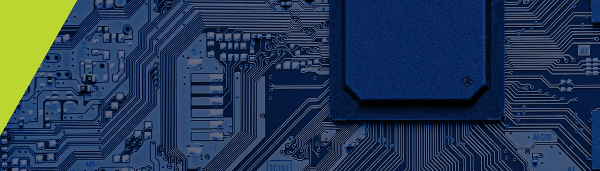
  • Basic Electronics and Microelectronics: Definitions of essential electronic terms/concepts and introduction to microelectronics and integrated circuits
  • Process Nodes: Process nodes and their impact on device performance and cost
  • Device Physics and Transistor Operation: Principles of device operation and transistor functionality
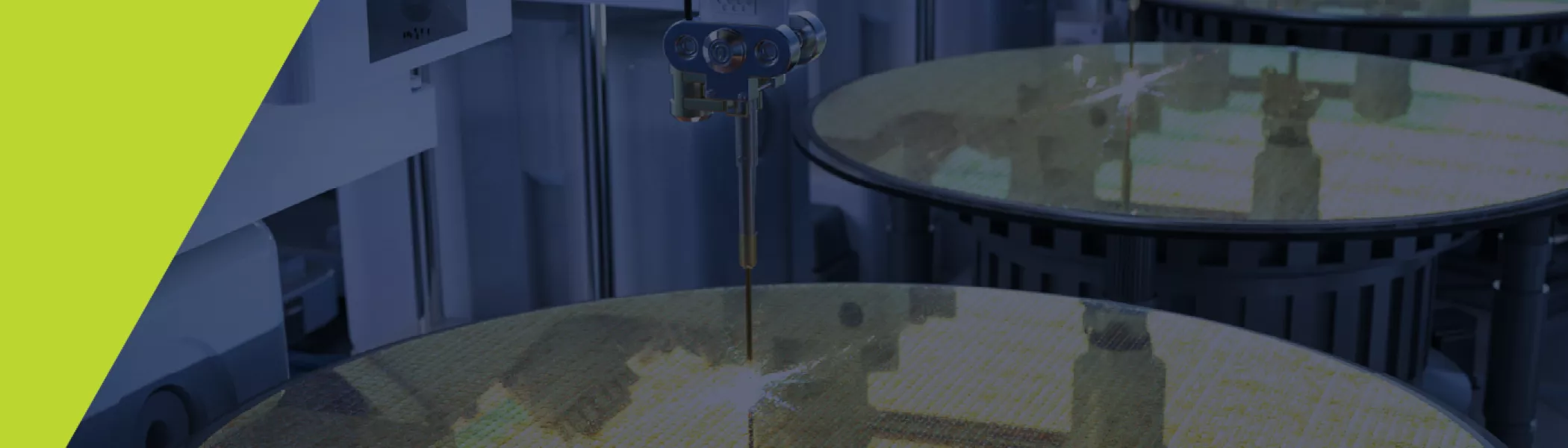
  • Crystal Growth and Wafer Preparation: Crystal growth techniques and wafer preparation processes
  • Advanced Transistor Technologies: FDSOI, FinFETs, and Gate-All-Around (GAA) transistors and their impact on device performance
  • Circuit Design and Layout: Introduction to circuit design, layout techniques, and tools
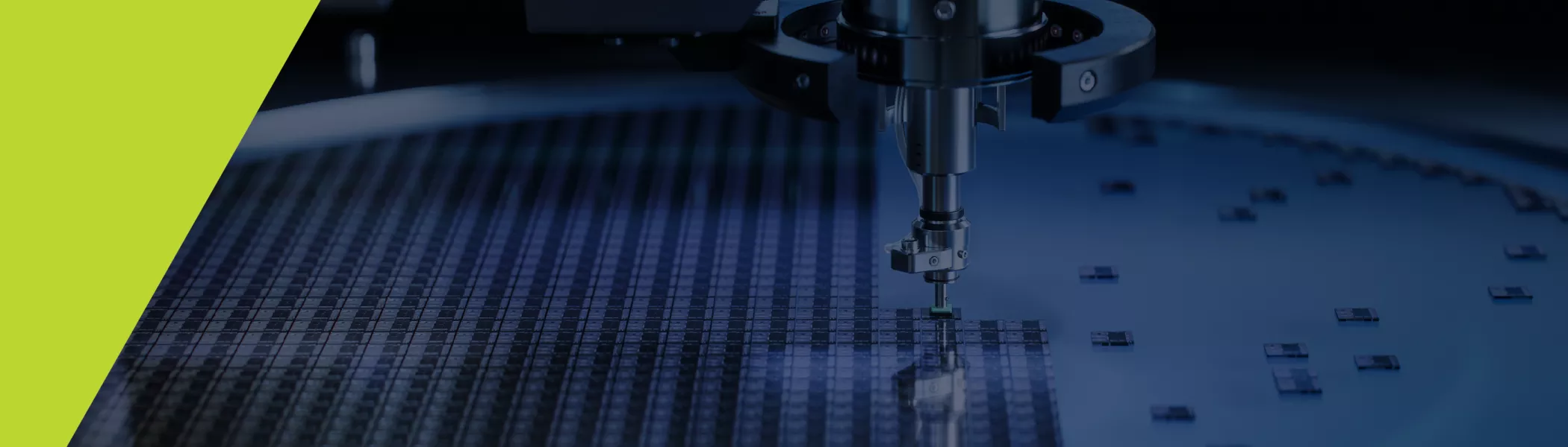
  • Wafer Processing:
    • Mask Making and Lithography: Techniques and materials used in mask making and various lithographic methods (DUV, Immersion, EUV)
    • Clean Room Environments: Importance of clean rooms in semiconductor manufacturing and contamination issues
    • Etching and Cleaning Processes: Plasma and wet etching processes
    • Ion Implantation and Diffusion Techniques: Methods for doping and controlling diffusion in semiconductor fabrication
    • Deposition Techniques: RTP, CVD, ALD, and ALE techniques and their effect on device performance
    • Electroplating and Sputtering: Metal deposition techniques used in manufacturing
    • Packaging and Testing: Techniques such as wire bonding, die stacking, flip chip, and chiplets packaging, semiconductor testing processes
    • Metrology and Measurement Tools: Tools and methods used for precision measurement in semiconductor manufacturing
  • Semiconductor Industry Ecosystem: The major players in the industry 

Who Should Attend

Anyone interested in understanding semiconductor manufacturing, including new employees, professionals in related industries, and those seeking to broaden their knowledge of the field.


Instructor

Denny Frye 

PT International, LLC

Instructor Bio

Important Information

Note that only the person who registered will receive a certificate of completion. This virtual training will not be recorded. Attendees must be present to access course knowledge. 

Can't find the training link day of? After you register, you will receive the link to the live training via the email address you provided. In addition, you will receive email reminders about 24 hours in an advance and an hour before with the same link. Please keep these emails on hand to access the trainings on time. If you do not see any confirmation emails, please check your junk/spam folders before contacting SEMI U for support.

United States

- SEMI U

Gain a comprehensive understanding of the semiconductor industry and the integrated circuit (IC) manufacturing process. This course is designed for new personnel in the field or anyone seeking a well-rounded knowledge of the tools, materials, and terminology used in semiconductor manufacturing.

Pricing
  • Members: $995
  • Non-Members: $1,095

* For group orders with 10+ attendees, and for Students/Veterans discounted pricing, please contact [email protected].

9:30 am - 5:00 pm Off Add to Calendar 2025-06-03 09:30:00 2025-06-04 17:00:00 Overview of Semiconductor Manufacturing (Virtual Training, US) Gain a comprehensive understanding of the semiconductor industry and the integrated circuit (IC) manufacturing process. This course is designed for new personnel in the field or anyone seeking a well-rounded knowledge of the tools, materials, and terminology used in semiconductor manufacturing.PricingMembers: $995Non-Members: $1,095* For group orders with 10+ attendees, and for Students/Veterans discounted pricing, please contact [email protected]. United States SEMI.org [email protected] America/Los_Angeles public America/Los_Angeles Closed
Event format
Promote in calendar
Off

Pioneering Digital Manufacturing Technology Will Revolutionize Semiconductor Packaging, Display Manufacturing, and Consumer Electronics

Las Vegas, US, January 8, 2025 – SCRONA AG, a leader in microfabrication technologies and the proud holder of a World Record for the smallest printed color picture, has unveiled its revolutionary 128-nozzle electrohydrodynamic (EHD) printhead at CES 2025. This groundbreaking innovation achieves a three-digit nozzle count in digital EHD technology for the first time, marking a major milestone that transforms EHD printing into a mass-production-ready solution.

Launching with a newly developed print engine for seamless integration into production tools by the end of Q1 2025, the 128-nozzle printhead is poised to revolutionize high-precision manufacturing across industries. "The rapid development from 8 to 48 and now to 128 nozzles in such a short time is a testament to the scalability of our MEMS-based EHD Gen-3 platform and execution of our team," said Dr. Patrick Galliker, CTO and Co-Founder of SCRONA.

A Leap in Digital Manufacturing for Key Industries

The SCRONA 128-nozzle printhead brings unprecedented precision, material flexibility, and scalability to industries such as semiconductor advanced packaging, display manufacturing, and consumer electronics. Key benefits and applications include:

1. Semiconductor Manufacturing:
- Revolutionary die-attach applications, dispensing ultra-small adhesive volumes with unparalleled accuracy.
- High-resolution printing of conductive interconnects, vital for advanced AI chiplets and chip manufacturing innovations.

2. Display Technology:
- Unmatched precision in applying quantum dots and color filters for next-generation micro-LED and OLED displays, enabling vibrant, energy-efficient screens.
- High-accuracy printing of adhesives and sealants for display packaging, facilitating thinner and flexible substrates.

3. Versatility Across Sectors:
- Enhanced printing capabilities for consumer electronics, defense, and life sciences, with the ability to print on curved or challenging substrates.
- A versatile solution surpassing the limitations of traditional inkjet and screen printing technologies.

Accelerating Mass Production Ready for EHD Technology

The introduction of the 128-nozzle printhead represents a paradigm shift in production technology, setting a new benchmark for accuracy, speed, and material flexibility. This innovation addresses the long-standing challenges of scaling EHD technology to meet the rigorous demands of high-volume manufacturing. "We are thrilled to unveil our 128-nozzle EHD printhead at CES 2025," said Dr. Patrick Heissler, CEO, SCRONA AG. "This breakthrough paves the way for manufacturers to achieve greater performance, miniaturization, and efficiency in production processes while unlocking new opportunities for innovation in advanced technologies."

About Scrona AG
Scrona is a spin-off from ETH Zurich, one of the top 10 global research universities. Scrona has developed the industry's first multi-nozzle printing platform that can digitally print with sub-micron precision, on any material and at scale. Its patented electrostatic printing technology is transforming manufacturing processes in the field of semiconductors, displays and many other products. It is enabling new designs not feasible for implementation with today’s processes while significantly reducing material, energy and water consumption.
Learn more at www.Scrona.com

From January 1, 2025 Heraeus is combining the high-performance materials expertise of Heraeus Conamic and Heraeus Comvance into a new operating company: Heraeus Covantics. The merged business will be led by a new management team. The legal entities will remain the same.

With the new operating company, Heraeus is further expanding its technology leadership in the manufacturing and processing of high-purity quartz, fused silica, and other high-end materials such as ceramics and innovative composites.

“We are creating a global powerhouse in which we drive innovation and exploit technological synergies,” explain Christoph Fark, Michael Werth and Nikolas Pojezny, Managing Directors of Heraeus Covantics. ”The new structure more closely aligns our combined capabilities and competencies with market requirements and customer needs. This enables our customers to strengthen their competitive advantage.”

Heraeus Covantics manufactures semi-finished products, complex system components and custom-tailored solutions made of quartz glass, fused silica and ceramic materials. They are used in the data transmission and telecommunication industry, the production of specialty optical fibers for industrial and medical applications, semiconductor manufacturing and optical applications among others.

About Heraeus
Heraeus is a family-owned global technology group headquartered in Hanau, Germany. The company’s roots go back to a family pharmacy started in 1660. With its expertise and resources, Heraeus has been making meaningful contributions over generations and is committed to do so in the future. Today, the group bundles diverse activities in four Business Platforms: Metals and Recycling, Healthcare, Semiconductor and Electronics, as well as Industrials. Customers benefit from innovative technologies and solutions based on broad materials knowledge and technological leadership. In the 2023 financial year, the group generated revenues of €25.6 billion (US$27.7 billion*) with approximately 16,400 employees in 40 countries. Heraeus is one of the top 10 family-owned companies in Germany.

About Heraeus Covantics
Heraeus Covantics is a technology leader specializing in the manufacturing and processing of the industry’s highest purity quartz, fused silica and other high-end materials such as ceramics and composites. With locations in Europe, USA and Asia, Heraeus Covantics manufactures semi-finished products, complex system components and custom-tailored solutions made of quartz glass, fused silica and ceramic materials. They are used in the data transmission and telecommunication industry, the production of specialty optical fibers for industrial and medical applications, semiconductor manufacturing and optical applications among others.

Registration

SEMI Members:  $49

Use your corporate email address during log in to be recognized as a SEMI Member.

Non-Members:  $99

Students:  Free

Contact Paul Cohen ([email protected]) with a picture of your student ID to receive your discount code.

Germany Japan Taiwan United States Savage on Security Webinar 2.jpg Technical
Highlighted content

Hardware is at the heart of computing systems. However, recent years have seen increased attacks exploiting hardware vulnerabilities and exploits, which even traditional software-based protections cannot prevent. Hardware fuzzing has shown promise in detecting vulnerabilities in large-scale designs like modern processors. In this talk, we will describe the hardware vulnerabilities in hardware description languages, such as Verilog and VHDL. Then, we will explain a new and radical approach called hardware fuzzing to find these vulnerabilities and detail how fuzzing techniques can be combined with existing formal verification techniques to detect vulnerabilities efficiently. Finally, we will discuss a strategy for pinpointing vulnerabilities to accelerate the mitigation process and briefly talk about improving the efficiency of hardware fuzzing using ML/AI techniques, such as multi-armed bandit (MAB) and large language models (LLM).

Meet the Speakers

Guest Speaker

Jeyavijayan (JV) Rajendran

Jeyavijayan (JV) Rajendran
Associate Professor
Department of Electrical and Computer Engineering
Texas A&M University
Biography

Moderator

Warren Savage

Warren Savage
Researcher at University of Maryland
Applied Research Laboratory for Intelligence and Security
Biography

United States

ESD Alliance

The ESD Alliance, a SEMI Technology Community, is hosting a webinar series, "Savage on Security," moderated by Warren Savage, Researcher at University of Maryland, Applied Research Laboratory for Intelligence and Security. 

10:00 am - 11:00 am Off Add to Calendar 2025-03-27 10:00:00 2025-03-27 11:00:00 ESD Alliance Webinar: Savage on Security 2: Mar 27, 2025 The ESD Alliance, a SEMI Technology Community, is hosting a webinar series, "Savage on Security," moderated by Warren Savage, Researcher at University of Maryland, Applied Research Laboratory for Intelligence and Security.  United States SEMI.org [email protected] America/Los_Angeles public Register Now to Watch the Recorded Event
Event format

Registration

Regular Pricing

SEMI Members: $100 | Non-Members: $125

United States REGISTER NOW Arizona Chapter Forum Thumbnail Business Executive

TRAVEL

ABB Logo 170x65
ASNA Logo 170x65
Arizona Technology Council Logo 170x65
Bodewell Group Logo 170x65
Edwards Vacuum Logo 170x65
EMD Electronics Logo 170x65
Rockwell Automation Logo 170x65
Skanska Logo 170x65
WGNSTAR
Vectara Logo 170x65

Become a Sponsor

Sponsorships can be tailored to meet your branding and marketing objectives. Become a sponsor and brand your company at the SEMI Arizona Breakfast Forum.

Contact Tim Janes, [email protected] to learn about available sponsorship opportunities.

Host— 


Playbook for Winning

Arizona’s semiconductor ecosystem is at an inflection point—poised to transform rapid growth into sustainable global leadership.  This forum convenes industry executives, policymakers and innovators to define strategies for making Arizona the premier global semiconductor resource.  The SEMI Arizona Breakfast Forum is where Arizona’s semiconductor current and future playbook is defined, designed to mobilize leadership towards actionable strategies helping evolve Arizona’s semiconductor industry into an international winning playbook.

Arizona’s Rapid Rise as America’s Semiconductor Headquarters has attracted major global companies, with more than 60 expansions and over $200 billion in new investments since 2020, including TSMC, Intel, and ASM, all of whom are expanding operations or building new fabs in AZ due to strong business climate, strategic location and infrastructure.  Statewide commitment through the Arizona Semiconductor Task Force, and the National Semiconductor Economic Roadmap (NSER) are enhanced by targeted incentives to attract companies and federal-state-industry alignments reinforce Arizona as a national leader in the next era of US semiconductor sovereignty. 

Join Us at Edwards Vacuum's Facility in Chandler to Learn More About—

  • Building the Premier Semiconductor Hub
  • Powering the Ecosystem—Infrastructure as the Foundation
    • The right strategy is critical to success.  Arizona’s must include water reliability, energy stability, long-term sustainability and cost-competitiveness.  The game plan must include sustainable growth at the scale demanded by advanced nodes, packaging and AI-driven manufacturing.   
  • Leading Regional & Global Supply Chain Resilience
  • Developing a World-Class Talent Team
  • Executive Panel Discussion—Investing in the Future: Capturing Long Range Goals


Questions?

Karen Popp—Sr. Program Manager, Programs & Committees
[email protected]

Edwards Vacuum
2411 E. Germann Rd.
Chandler, AZ 95286
United States

7:30 am - 8:00 am

Check-In and Breakfast

Edwards Vacuum Logo 170x65
8:00 am - 8:10 am

Welcome Remarks—Arizona Chapter

8:10 am - 8:20 am
Lee Short, Edwards Vacuum
Lee Short
General Manager, Service Technology Centers
Edwards Vacuum

Welcome Remarks—Edwards Vacuum

8:20 am - 8:40 am
Kevin Hartke, Mayor of Chandler, Arizona
Kevin Hartke
Mayor
City of Chandler, Arizona

Keynote

8:40 am - 9:10 am
Brad Perkins, EMD Electronics
Brad Perkins
Head of Global Product Management
EMD Electronics

Building the Premier Semiconductor Hub—Turning Arizona's Momentum into a Consistent, Competitive Advantage

Biography

Arizona is evolving from rapid expansion to ecosystem integration, ensuring every piece of the value chain connects efficiently. All the fundamental components, from research institutions to logistics and infrastructure partners to materials suppliers, packaging facilities to fabs are fundamental elements to this integration.

9:10 am - 9:40 am
Kathryn Sorensen, ASU
Kathryn Sorensen, PhD
Director of Research & Professor of Practice, Kyl Center for Water Policy at Morrison Institute;
Senior Global Futures Scientist, Arizona State University

Powering the Ecosystem—Infrastructure as the Foundation - Water Resources

9:40 am - 10:10 am
Michael Eugenis, Arizona Public Service
Michael Eugenis, PE
Director of Resource Planning
Arizona Public Service

Powering the Ecosystem—Infrastructure as the Foundation - Power Resources

10:10 am - 10:25 am

Networking Break

10:25 am - 10:55 am
Jennifer Jacques, Schneider Electric
Jennifer Jacques
VP, North America Supply Chain
Schneider Electric

Leading Regional & Global Supply Chain Resilience

Biography

Arizona is leading the way in becoming the most resilient, efficient semiconductor hub in North America. Through diversified sourcing, regional collaboration, logistics optimization, and flexible, shock-resistant supply models, Arizona will lead the way. Deployment of automated mitigation workflows, enabling alternate-site activation and faster recovery. Strong emphasis on transparent supplier collaboration, including exchange of validated data across tiers down to parts and materials.

10:55 am - 11:15 am
Olga Teran, Arizona Commerce Authority
Olga Teran
Workforce Program Manager
Arizona Commerce Authority

Developing a World-Class Talent Team

Biography

Arizona’s strategic success depends upon its ability to produce, attract, and retain top-tier semiconductor talent. This plan includes investment in semiconductor training programs, securing next-gen engineering talent, research partnerships, on-the-job R&D exposure, and providing retraining and upscaling pathways.

Investment in semiconductor training programs, securing next-gen engineering talent, research partnerships, on-the-job R&D exposure, and providing retraining and upscaling pathways.

11:15 am - 11:40 am
Mike Glavin
Mike Glavin
Program Director, Workforce Development
SEMI Foundation

Workforce Development

11:40 am - 12:15 pm
Steven G. Zylstra, Arizona Technology Council
MODERATOR
Steven G. Zylstra
President and CEO
Arizona Technology Council and SciTech Institute
Lalitha Immaneni, Intel
Lalitha Immaneni
Vice President, Architecture, Advanced Design and Customer Enabling, Technology Development
Intel
Rich Simoncic, Microchip Technology
Richard Simoncic
Chief Operating Officer
Microchip Technology
Nasser Peyghambarian, University of Arizona
Nasser Peyghambarian, PhD
Professor of Optical Sciences and Materials Science and Engineering
University of Arizona

Executive Panel Discussion: Investing in the Future—Capturing Long Range Goals

The winning strategy will continue to require accelerated investments in R&D, creating new labs and testing capabilities, advanced packaging pilot lines, next-gen university research facilities, and sustainable infrastructure. Arizona is positioned to attract investments and to remain a market leader in 2026, 2030, and beyond.

Steven G. Zylstra, President and CEO, Arizona Technology Council and SciTech Institute

Lalitha Immaneni, Vice President, Architecture, Advanced Design and Customer Enabling, Technology Development, Intel

Richard Simoncic, Chief Operating Officer, Microchip Technology

Nasser Peyghambarian, PhD, Professor of Optical Sciences and Materials Science, University of Arizona

12:15 pm - 12:30 pm

Q&A

12:30 pm

Adjourn

12:30 pm - 1:30 pm

Tour of Edwards Facility

SEMI Breakfast Forum Organized by SEMI Arizona Chapter

In-Person | Arizona Time

7:30 am - 12:30 pm Off Add to Calendar 2026-05-06 07:30:00 2026-05-06 12:30:00 SEMI Arizona Breakfast Forum SEMI Breakfast Forum Organized by SEMI Arizona ChapterIn-Person | Arizona Time Edwards Vacuum 2411 E. Germann Rd. Chandler, AZ 95286 United States SEMI.org [email protected] America/Los_Angeles public America/Los_Angeles 2
Event format
Promote in calendar
Off

WILMINGTON, Del., Dec. 18, 2024 – DuPont (NYSE: DD) today announced it has joined the SEMI Foundation’s Semiconductor PRIDE (Semiconductor Professionals for Respect, Inclusion, Diversity, and Equity) initiative as a Founding Member. Semiconductor PRIDE, which launched earlier this year, is a coalition of companies who are committed to advancing LGBTQ+ equity and inclusion in the semiconductor workforce.

The Semiconductor Industry Association (SIA) projects that 58% of new semiconductor manufacturing and design jobs in the U.S. risk going unfilled by 2030 (SIA, 2023). This potential talent gap, along with shifting demographics where one in five Generation Z adults in the U.S. identifies as LGBTQ+, highlights the need to reevaluate strategies for preparing the future workforce (Gallup, 2024). Semiconductor PRIDE is a new working group within the SEMI Foundation, the workforce development arm of SEMI, that aims to broaden workforce development efforts to advance LGBTQ+ inclusion.

“Joining Semiconductor PRIDE reaffirms our commitment to fostering an inclusive supportive environment for LGBTQ+ employees and allies,” said Devon Benedict, Integrated Operations Program Leader, DuPont, and Events and Partnerships Co-Chair for the DuPont Pride employee network. “This partnership promotes the attraction of LGBTQ+ talent in the semiconductor workforce and is a natural fit with our values.”

The DuPont Pride network was instrumental in having the company join the SEMI Foundation’s efforts. Established in 1991, DuPont Pride embodies the company’s longstanding commitment to promote an inclusive, diverse, and innovative work environment. This is reflected in the company achieving a perfect score on the Human Rights Campaign Foundation’s Corporate Equality Index, the foremost benchmark for corporate policies and practices related to LGBTQ+ workplace equality in the U.S.

In collaboration with industry partners, DuPont is committed to not only closing the talent gap in the semiconductor industry but also ensuring that every individual has the opportunity to thrive in an inclusive environment.

About SEMI
SEMI® is the global industry association connecting over 3,000 member companies and 1.5 million professionals worldwide across the semiconductor and electronics design and manufacturing supply chain. We accelerate member collaboration on solutions to top industry challenges through Advocacy, Workforce Development, Sustainability, Supply Chain Management and other programs. Our SEMICON® expositions and events, technology communities, standards and market intelligence help advance our members’ business growth and innovations in design, devices, equipment, materials, services and software, enabling smarter, faster, more secure electronics. Visit www.semi.org, contact a regional office, and connect with SEMI on LinkedIn and X to learn more.

About DuPont
DuPont (NYSE: DD) is a global innovation leader with technology-based materials and solutions that help transform industries and everyday life. Our employees apply diverse science and expertise to help customers advance their best ideas and deliver essential innovations in key markets including electronics, transportation, construction, water, healthcare and worker safety. More information about the company, its businesses and solutions can be found at www.dupont.com. Investors can access information included on the Investor Relations section of the website at investors.dupont.com.