downloadGroupGroupnoun_press release_995423_000000 copyGroupnoun_Feed_96767_000000Group 19noun_pictures_1817522_000000Member company iconResource item iconStore item iconGroup 19Group 19noun_Photo_2085192_000000 Copynoun_presentation_2096081_000000Group 19Group Copy 7noun_webinar_692730_000000Path
Skip to main content
Default Banner Image

United States

MILPITAS, Calif. – May 19, 2025 – According to the Q1 2025 Semiconductor Manufacturing Monitor (SMM) Report released by SEMI in collaboration with TechInsights, the global semiconductor manufacturing industry entered 2025 with typical seasonal patterns. However, looming tariff threats and evolving supply chain strategies are expected to create atypical seasonality for several industry segments as the year progresses.

Despite heightened trade policy risks, current data for the first quarter of 2025 indicate that electronics and integrated circuit (IC) sales have not been directly impacted by the newly announced tariffs. Electronics sales declined 16% quarter-over-quarter (QoQ) in Q1 2025 and remained flat year-over-year (YoY), consistent with traditional seasonal patterns. IC sales contracted by 2% QoQ but posted a robust 23% YoY increase, reflecting ongoing investment in AI and high-performance computing infrastructure.

semi & techinsights
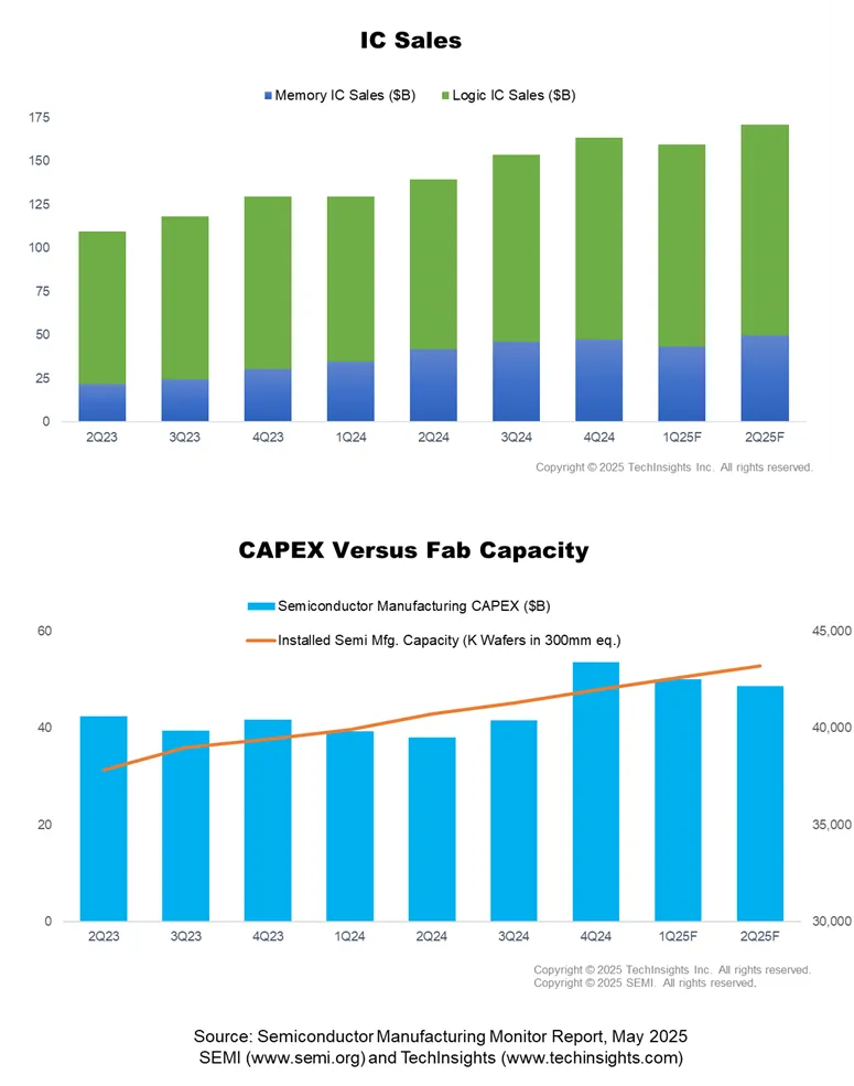
“While the first quarter of 2025 did not see a direct impact from new tariffs on electronics and IC sales, the uncertainty around global trade policies is prompting some companies to accelerate shipments and others to pause investments,” said Clark Tseng, Senior Director of Market Intelligence at SEMI. “This push-pull dynamic could lead to atypical seasonality for the remainder of the year as the industry adapts to shifting supply chain and tariff landscapes.”

Semiconductor capital expenditures (CapEx) declined 7% QoQ but surged 27% YoY, as manufacturers continued to invest heavily in leading-edge logic, high-bandwidth memory (HBM) and advanced packaging to support AI-driven applications. Memory-related CapEx soared 57% YoY in Q1 2025, while non-memory CapEx expanded by 15% YoY, underscoring the industry’s focus on innovation and resilience.

Wafer fab equipment (WFE) spending rose 19% year-over-year in Q1 2025 and is projected to increase another 12% in Q2, driven by strong investments in advanced logic and memory production to support the rapid adoption of AI semiconductors. Test equipment billings surged 56% year-over-year in Q1 and are expected to grow by 53% in Q2, reflecting the heightened complexity and stringent performance requirements of AI and HBM chip testing. Assembly and packaging equipment also registered double-digit growth, benefiting from the industry’s push toward higher-density integration and advanced packaging solutions.

“The WFE market is poised for steady growth driven by government investments and semiconductor advancements, particularly in AI and emerging technologies,” said Boris Metodiev, Director of Market Analysis at TechInsights. “However, geopolitical uncertainties, including export restrictions and potential tariffs, pose significant risks that could impact this positive trajectory.”

Aligned with the growth in capital equipment investments, global installed wafer fab capacity is on the rise and is projected to surpass 42.5 million wafers per quarter (in 300mm wafer equivalents), reflecting a 2% QoQ and 7% YoY increase in Q1 2025. China continues to lead all regions in capacity expansion, though the pace of growth is expected to moderate in the coming quarters. Notably, Japan and Taiwan are experiencing the strongest quarterly capacity gains, driven by significant investments in power semiconductor manufacturing in Japan and the ramp-up of a leading-edge foundry in Taiwan.

Looking ahead, SEMI and TechInsights expect the industry to experience atypical seasonal patterns in 2025 as companies navigate the dual challenges of trade policy uncertainty and supply chain adaptation. While demand for AI and data center technologies remains a bright spot, other segments may see delayed investment or demand shifts as the market responds to evolving tariff and geopolitical uncertainties.


The Semiconductor Manufacturing Monitor (SMM) report provides end-to-end data on the worldwide semiconductor manufacturing industry. The report highlights key trends based on industry indicators including capital equipment, fab capacity, and semiconductor and electronics sales, and includes a capital equipment market forecast. The SMM report also contains two years of quarterly data and a one-quarter outlook for the semiconductor manufacturing supply chain including leading IDM, fabless, foundry, and OSAT companies. An SMM subscription includes quarterly reports. 

Download a sample Semiconductor Manufacturing Monitor report.  

For more information on the report or to subscribe, please contact the SEMI Market Intelligence Team at [email protected]. Details on SEMI market data are available at SEMI Market Data.  

About SEMI

SEMI® is the global industry association connecting over 3,000 member companies and 1.5 million professionals worldwide across the semiconductor and electronics design and manufacturing supply chain. We accelerate member collaboration on solutions to top industry challenges through Advocacy, Workforce Development, Sustainability, Supply Chain Management and other programs. Our SEMICON® expositions and events, technology communities, standards and market intelligence help advance our members’ business growth and innovations in design, devices, equipment, materials, services and software, enabling smarter, faster, more secure electronics. Visit www.semi.org, contact a regional office, and connect with SEMI on LinkedIn and X to learn more.

Association Contact

Sherrie Gutierrez/SEMI
Phone: 1.831.889.3800 
Email: [email protected]

Maulburg / Blaubeuren, May 13, 2025 – The Busch Group, one of the largest vacuum solution providers worldwide, announces that its brand centrotherm clean solutions will become part of Pfeiffer Vacuum+Fab Solutions. Effective September 2025, the gas abatement systems for the semiconductor industry previously offered under this brand will be integrated into the Pfeiffer portfolio and be available under this name in the future, uniting the two members of the global Busch Group.

Cutting-edge fab solutions from a trusted brand
By consolidating the product portfolio of centrotherm clean solutions under a single, unified brand, customers will benefit from the convenience of sourcing high-quality vacuum solutions for the semiconductor industry and related sectors from a one-stop, trusted supplier.

Within the Group, Pfeiffer Vacuum+Fab Solutions is the renowned brand for high and ultra-high vacuum, providing innovative, cutting-edge solutions for demanding applications in research and development, analytics, industry, and semiconductor. Sami Busch, Co-Owner and Co-CEO of the Busch Group, states: “Bringing our product portfolio for the semiconductor industry together under our strong and well-established brand Pfeiffer Vacuum+Fab Solutions further streamlines our product offering. This enhances our ability to serve semiconductor and related industries with high-quality end-to-end solutions – not only for vacuum generation but also for related critical applications such as leak detection or contamination management. This step underscores our commitment to delivering exceptional value and support to our customers worldwide.”

Comprehensive portfolio for the semiconductor market
Busch acquired centrotherm clean solutions in 2023, implementing its industry-leading gas abatement expertise into its broader portfolio. The products now being integrated into the Pfeiffer brand are primarily used in the semiconductor industry but also, for example, in the production of MEMS, LEDs, solar cells, and flat panel displays. The offering comprises standardized gas abatement systems as well as individual customized systems and overall environmental solutions.
All 350 centrotherm clean solutions employees will retain their positions and contracts, ensuring stability for both staff as well as customers while at the same time guaranteeing continued expertise, seamless service, and uninterrupted availability. The main office and production plant for abatement systems will remain in Blaubeuren in Baden-Württemberg.

About the Busch Group
The Busch Group is one of the world’s largest manufacturers of vacuum pumps, vacuum systems, blowers, compressors and gas abatement systems. Under its umbrella, the group houses two well-known brands: Busch Vacuum Solutions and Pfeiffer Vacuum+Fab Solutions. The gas abatement systems previously offered by centrotherm clean solutions – a former Busch Group brand – are now part of the Pfeiffer portfolio.
The extensive product and service offer includes solutions for vacuum, overpressure and abatement applications in all industries, such as food, semiconductors, analytics, chemicals and plastics. This also includes the design and construction of tailor-made vacuum systems and a worldwide service network.

The Busch Group is a family business that is managed by the Busch family. More than 8,000 employees in 44 countries worldwide work for the group. Busch is headquartered in Maulburg, Baden-Württemberg, in the tri-country region of Germany, France and Switzerland.

The Busch Group manufactures in its 23 own production plants in China, the Czech Republic, France, Germany, India, Romania, South Korea, Switzerland, the United Kingdom, the USA and Vietnam.

The Busch Group has an annual consolidated revenue of close to 2 billion Euro.

Media Contact
Dr Fabian Fahlbusch
Head of Content and Communications
Busch Vacuum Solutions
Schauinslandstrasse 1
D-79689 Maulburg, Germany

+49 (0)7622 681 - 3379
[email protected]
www.buschvacuum.com
www.buschgroup.com

Singapore, May 12, 2025 - DuPont (NYSE: DD) is excited to announce its participation in SEMICON Southeast Asia (SEMICON SEA), taking place May 20-22, 2025, in Singapore. At booth L3105, DuPont will showcase the latest offerings of Kalrez® perfluoroelastomer parts specifically designed for semiconductor and electronics applications, aimed at enhancing manufacturing efficiency and operational sustainability.

“Our new Kalrez® product offerings are engineered for enhanced sealing performance, significantly reducing leaks and pumping times,” said Dr. Meredith Dunbar, Kalrez® Global Technology Leader, DuPont. “In our continuous pursuit of sustainability, we have achieved improvements in sealing performance under harsh process conditions, which enable substantial waste reduction. These advancements make Kalrez® seals an ideal choice for the toughest challenges in semiconductor fabs, and also showcase our dedication to delivering high-quality, efficient, and environmentally responsible solutions.”

Highlighting this longstanding commitment to innovation, the Kalrez® brand is proud to celebrate its 50th anniversary this year. This milestone reflects five decades of excellence and dedication to developing high-performance sealing solutions tailored for critical applications in demanding environments. At this year’s SEMICON SEA exhibition, attendees will discover several key advancements, including:

Kalrez® Bonded Door Seal (BDS): Specifically designed for semiconductor manufacturing equipment, including applications like plasma etching, CVD, and PVD, Kalrez® BDS offers improved sealing performance over conventional O-rings by reducing particle generation, extending seal life, and minimizing maintenance downtime.

Bonding Methodology: An innovative bonding method developed by DuPont's technology team, allowing Kalrez® components to be fused with other functional materials, creating unique, composite-structured Kalrez® parts.

Custom Shaped Parts: Kalrez® custom perfluoroelastomer parts can be tailored to unique geometries for specific sealing applications and are available in various shapes and compounds to meet different thermal, chemical, and plasma resistance requirements. Custom parts can be produced as both volume production and prototypes.

DuPont is proud to be driving technological advancements in the Kalrez® product family and providing game-changing solutions to its customers worldwide. All SEMICON SEA attendees are invited to join in celebrating the 50th anniversary of Kalrez® and explore how Kalrez® products can support their innovation programs.

For more information about Kalrez® parts and applications, please visit www.kalrez.com.

About DuPont

DuPont (NYSE: DD) is a global innovation leader with technology-based materials and solutions that help transform industries and everyday life. Our employees apply diverse science and expertise to help customers advance their best ideas and deliver essential innovations in key markets, including electronics, transportation, construction, water, healthcare, and worker safety. More information about the company, its businesses, and solutions can be found at www.dupont.com. Investors can access information included on the Investor Relations section of the website at investors.dupont.com.

#   #   #

05/12/25

DuPont™, the DuPont Oval Logo, and all trademarks and service marks denoted with ™, ℠ or ® are owned by affiliates of DuPont de Nemours, Inc. unless otherwise noted. 

For further information, contact:

Rebekah Lazar
Semiconductor Technologies Communications Leader
DuPont
[email protected]

Cell: +1-302-509-1859

United States https://www.semiconwest.org/ SCW-Graphics_Reg_360x317@2_SCW_Event Tile_1.jpg Business Executive Expositions
Highlighted content

San Francisco, CA
United States

- APHI CAST EHS NBMC SCM Smart MFG Smart Mobility Smart MedTech Smart Data & AI SMG Sustainability EMG ESD Alliance FlexTech FOA ITL MSIG SCIS SE&A SiPAT SOI Standards Workforce Development Off Add to Calendar 2026-10-13 00:00:00 2026-10-15 00:00:00 SEMICON West 2026 San Francisco, CA United States SEMI.org [email protected] America/Los_Angeles public
Event format
Promote in calendar
Off

Registration

SEMI Members:  $49

Use your corporate email address during log in to be recognized as a SEMI Member.

Non-Members:  $99

Students:  Free

Contact Paul Cohen ([email protected]) with a picture of your student ID to receive your discount code.

Germany Taiwan United States Intro to Design and EDA Recorded Event.jpg Technical Training
Highlighted content

The chips powering today’s cell phones, cars, computers, and more can contain billions of transistors. Designing these chips requires a team of engineers with expertise in various aspects of the design flow, along with Electronic Design Automation (EDA) tools that are needed to implement and verify these complex designs.

This Master Class is intended for non-technical staff that wish to understand the basics of semiconductor chip design. It provides an appreciation of the complex design flows and an understanding of some of the terminology used by chip design teams.

For students, the course will introduce some of the rewarding challenges and career opportunities available in the design and EDA industries.

In this class we will cover basic information about digital chips, then introduce some of the key steps and tools used during the design flow. We will also discuss some of the tradeoffs of different implementation methodologies and some of the challenges presented by various critical applications such as devices used in medical and automotive systems.
 

10:00 am - 10:05 am
Gity Samadi
Gity Samadi
Sr. Director of R&D Programs
SEMI

Welcome and Introduction

10:05 am - 11:30 am
Paul Cohen
Paul Cohen
Sr. Manager, ESDA
SEMI

Introduction to Chip Design and EDA

Biography

Course Overview
• Introduction to electronic devices
• Overview of digital logic and chip design history
• Semiconductor manufacturing basics
• Chip design and verification flow
• Implementation choices
• Heterogenous integration
• Interface to manufacturing
• Emerging challenges

Smart MFG ESD Alliance FOA SOI

Complex semiconductor chips power today’s cell phones, cars, computers, and more. This on-line Master Class will provide non-technical people who work in and around the chip design industry a high-level overview and understanding of how these complex chips are designed. 

10:00 am - 11:30 am Off Add to Calendar 2025-06-25 10:00:00 2025-06-25 11:30:00 ESD Alliance Master Class: Introduction to Design and EDA Complex semiconductor chips power today’s cell phones, cars, computers, and more. This on-line Master Class will provide non-technical people who work in and around the chip design industry a high-level overview and understanding of how these complex chips are designed.  SEMI.org [email protected] America/Los_Angeles public America/Los_Angeles Register Now to Watch the Recorded Event
Event format
Promote in calendar
Off

Tokyo Electron U.S. Celebrates its New Headquarters in the Heart of Austin 

The semiconductor equipment manufacturer has operated in the U.S. for over 30 years.

Austin, Texas, April 16th, 2025 –Toshiki Kawai, Tokyo Electron (TEL) President & CEO cut the ribbon at the company’s new TEL | RiverSouth HQ, signaling a new era for the organization that has played a crucial part in the U.S. semiconductor and technology landscape for over three decades. 

“With Tokyo Electron's pivotal role in the U.S. semiconductor industry, it is only fitting that our office is located in the dynamic center of Austin,” said Bobby Shirai, President of Tokyo Electron U.S. Holdings. “The U.S. has long been a hub for intellectual and research capital and serves as the beating heart of global technology. We are a partner and ally committed to America’s innovative tech future.” 

Tokyo Electron U.S. manages 19 sites, employing nearly 3,400 people across the United States, with over 600 employees in Austin. The company leads the world in patents within the semiconductor production equipment industry, underscoring its commitment to innovation and excellence.

Texas Secretary of State Jane Nelson, the Consulate-General of Japan in Houston Zentaro Naganuma, Samsung Austin Semiconductor. Vice President Jon Taylor, Austin Chamber of Commerce President & CEO Jeremy Martin, and President and Tokyo Electron America President Mark Dougherty also joined the opening and recognized how the importance of the new headquarters will be in facilitating greater collaboration across sectors. 

About Tokyo Electron U.S.

Tokyo Electron (TEL) U.S. is the American subsidiary of Tokyo Electron and U.S. headquarters and one of the world’s leading producers of semiconductor production equipment. Headquartered in Austin, Texas for over 30 years, TEL U.S. is proud to employ almost 3,600 people across the United States who are contributing to technological innovation in semiconductors. Learn more about how TEL’s research and development stands at the cutting edge of innovation for Technology Enabling Life: About TEL | Tokyo Electron Ltd.


Registration

SEMI Members: FREE
Use your corporate email address during log in to be recognized as a SEMI Member.

Non-Members:
Early-Bird Pricing: $40
Regular Pricing (begins May 22): $50

United States Exec Outlook Event Page Tile update.jpg Business Executive Technical

Event Host

Highlighted content

How Will Agentic AI Change Chip Design and Verification?” features EDA and emerging agentic AI company executives and entrepreneurs discussing changes within chip design and verification as agentic AI tools become more mainstream. Panelists will distill the excitement surrounding the innovation in chip design and verification, collaboration between traditional EDA and agentic AI startups and broader implications for technological advancements.

Cadence Design Systems
2655 Seely Avenue
San Jose, CA 95134
United States

5:30 pm - 6:45 pm

Registration and Networking with Dinner and Beverages

6:45 pm - 7:00 pm
Julie Rogers
Julie Rogers
Executive Director
ESD Alliance
Chuck Alpert
Chuck Alpert
Fellow
Cadence

Welcome and Speaker Introductions

7:00 pm - 8:30 pm
Ed Sperling
Moderator
Ed Sperling
Editor-in-Chief
Semiconductor Engineering
Dave Kelf
Dave Kelf
CEO
Breker Verification Systems
Wally Rhines
Walden Rhines
CEO
Silvaco
Vince Wong
Vince Wong
Head of AI Development
Verific
Shelly Henry
Shelly Henry
CEO
Moores Lab AI
Ann Wu
Ann Wu
CEO
Silimate
Cindy Cui
Cindy Cui
VP of Global Customer Success
ChipAgents
ESD Alliance

Join ESDA for our Executive Outlook event, "How Will Agentic AI Change Chip Design and Verification?"

5:30 pm - 8:30 pm Off Add to Calendar Disabled America/Los_Angeles Register Now!
Event format
Tab Order
Overview
Agenda
Registration
New Tab 1
Travel
Sponsors
Call for Abstracts
Call for Papers
Technology Showcase
Press
New Tab 2
Photo Gallery
Promote in calendar
Off

DuPont’s semiconductor materials innovation recognized in category for AI-driven advancements

WILMINGTON, Del., April 8, 2025 – DuPont (NYSE:DD) today announced that its Ikonic™ 9000 series of polishing pads for chemical mechanical planarization (CMP) was awarded a 2025 Bronze Edison Award™ in the AI-driven advancements category.

The Ikonic™ 9000 CMP pad series is a new expansion to DuPont’s Ikonic™ CMP product family, developed to enhance productivity and sustainability in semiconductor manufacturing processes for advanced chips. Ikonic™ 9000 pads have been recognized alongside other semiconductor innovations for AI and high-performance computing.

“Customers frequently turn to DuPont to tackle their next-generation technology challenges through advanced semiconductor materials,” said Sang Ho Kang, Vice President and General Manager, DuPont Semiconductor Technologies. “The development of Ikonic™ 9000 series pads is a successful outcome from addressing two critical needs for advanced node manufacturing—enhanced performance and more sustainable operations.”

Ikonic™ 9000 pads offer a high removal rate in CMP that leads to increased process throughput, and an advanced groove design aimed at maximizing slurry efficiency. At advanced fabrication nodes for chips supporting AI and high-performance computing, increased process complexity makes CMP efficiency especially important.

Additionally, the pads exhibit a longer operational life due to low wear rates, allowing for less frequent replacements and reduced downtime, optimizing production workflows. These features not only improve productivity, but also minimize waste, creating a more sustainable solution for semiconductor fabs.

“We are excited to see such a strong industry response to the launch of Ikonic™ 9000 pads, because they represent the start of a new wave of CMP innovation for performance, efficiency and sustainability,” said Randal King, Ph.D., Vice President of R&D/Technology, DuPont Electronics & Industrial. “DuPont is proud to be driving innovation across multiple new CMP pad and subpad families, and we look forward to launching more next-generation CMP pads to support advanced computing and AI.”

The Edison Awards™ is an annual competition honoring excellence in new product and service development, marketing, human-centered design, and innovation. Winners were selected from thousands of submissions and announced at the Edison Awards Gala in Fort Meyers, Florida on Thursday, April 3, 2025.

Ikonic™ 9000 series CMP pads have been successfully placed at advanced technology nodes. Customers interested in learning more about Ikonic™ 9000 CMP pads or other opportunities to drive sustainability enhancements in their CMP processes should contact their DuPont account manager.

sigma design logo

Sigma Design Joins SEMI to Support Semiconductor and Electronics Industries

(April 1, 2025) - Camas, WA - Sigma Design, Inc., a leader in product development and engineering, is pleased to announce its membership in SEMI, the global industry association representing the semiconductor and electronics design and manufacturing supply chain.

By joining SEMI, Sigma Design gains access to an extensive network of industry leaders, market insights, and collaborative connections that enhance opportunities to deliver support services for semiconductor manufacturing, material handling and testing. This membership aligns with Sigma Design’s commitment to advancing technology and contributing to the growth of the semiconductor ecosystem.

Sigma Design is committed to driving innovation and excellence in support of the semiconductor industry. “Joining SEMI represents a significant step in that journey," said Yehudit Dagan, Director of Sales and Marketing at Sigma Design. “This membership will enable us to stay at the forefront of industry trends, enhance our support services for other SEMI members, and strengthen our ties with this community.”

As a SEMI member, Sigma Design looks forward to leveraging the organization’s resources to support the growth of the semiconductor ecosystem and reinforce its position as a trusted partner in the industry.

About Sigma Design

As product development experts, we are driven by new challenges. We design, engineer, build, and test solutions for our partners' success. Sigma Design is a full-service product development and engineering firm dedicated to solving complex challenges. With a focus on quality, efficiency, and innovation, Sigma Design provides end-to-end product development solutions that encompass design, engineering, manufacturing, testing, and staffing services. Committed to excellence, we exceed client expectations with our dedicated approach. Challenges Accepted. Solutions Delivered.


For more information, visit www.sigmadzn.com

About SEMI

SEMI® is the global industry association connecting over 3,000 member companies and 1.5 million professionals worldwide across the semiconductor and electronics design and manufacturing supply chain. We accelerate member collaboration on solutions to top industry challenges through Advocacy, Workforce Development, Sustainability, Supply Chain Management and other programs. Our SEMICON® expositions and events, technology communities, standards and market intelligence help advance our members’ business growth and innovations in design, devices, equipment, materials, services and software, enabling smarter, faster, more secure electronics. Visit www.semi.org, contact a regional office, and connect with SEMI on LinkedIn and X to learn more.  

United States AMF webinar graphic Training
Highlighted content

Andrew Fung, A. M. Fitzgerald and Associates

Andrew O. Fung, Ph.D., Director of Business Development, A.M. Fitzgerald & Associates LLC 

Dr. Fung advances product development programs for MEMS-enabled microsystems. He has 25 years of multinational experience in industry teams and research, with broad awareness of integrated microsystems. His track record covers technology innovation, collaborative research, community building, fundraising, and mentorship. Prior to joining AMFitzgerald, Dr. Fung was Team Leader of MEMS, Nanofabrication, and Integration at CMC Microsystems, and Scientific Advisor to Aterica Health Inc. Dr. Fung received his B.A.Sc. in Electrical Engineering from University of Waterloo and Ph.D. in Biomedical Engineering from University of California, Los Angeles.

United States

NBMC FlexTech MSIG

Hosted by SEMI MSIG

The global medical device market is poised to benefit from miniature sensors that enable increasing instrumentation for data acquisition. Wearable health monitors, precision surgical tools, active implantables, and point-of-care diagnostics continue to drive demand for sensorization. As medtech companies race to innovate, MEMS-based solutions are revolutionizing patient care—enabling real-time monitoring, improving clinical outcomes, and reducing healthcare costs. Join A.M. Fitzgerald & Associates in this webinar to explore cutting-edge intersections of MEMS and healthcare, from wearable biosensors and intelligent implants to breakthrough microfluidic diagnostics. This session will highlight emerging technology opportunities and key challenges, providing actionable insights for medtech innovators looking to accelerate product development and scale MEMS-enabled devices successfully. 

What You’ll Learn: 

✔ Market trends shaping the future of MEMS in medtech 

✔ How MEMS sensors are transforming patient monitoring and intervention 

✔ Strategies for overcoming design, manufacturing, and regulatory hurdles 

✔ Examples of A.M. Fitzgerald innovations in MEMS-enabled medtech products 


Who Should Attend? 

Medtech executives, product managers, R&D leaders, engineers, innovators, and MEMS enthusiasts eager to see how MEMS technology is being integrated into next-generation healthcare solutions. 


Don’t miss this opportunity to gain a competitive edge in the fast-evolving medtech landscape! 

Register Now to secure your spot.

8:00 am - 9:00 am Off Add to Calendar 2025-05-07 08:00:00 2025-05-07 09:00:00 A.M. Fitzgerald Webinar - Empowering Tomorrow’s Precision MedTech with Sensor Solutions Hosted by SEMI MSIGThe global medical device market is poised to benefit from miniature sensors that enable increasing instrumentation for data acquisition. Wearable health monitors, precision surgical tools, active implantables, and point-of-care diagnostics continue to drive demand for sensorization. As medtech companies race to innovate, MEMS-based solutions are revolutionizing patient care—enabling real-time monitoring, improving clinical outcomes, and reducing healthcare costs. Join A.M. Fitzgerald & Associates in this webinar to explore cutting-edge intersections of MEMS and healthcare, from wearable biosensors and intelligent implants to breakthrough microfluidic diagnostics. This session will highlight emerging technology opportunities and key challenges, providing actionable insights for medtech innovators looking to accelerate product development and scale MEMS-enabled devices successfully. What You’ll Learn: ✔ Market trends shaping the future of MEMS in medtech ✔ How MEMS sensors are transforming patient monitoring and intervention ✔ Strategies for overcoming design, manufacturing, and regulatory hurdles ✔ Examples of A.M. Fitzgerald innovations in MEMS-enabled medtech products  Who Should Attend? Medtech executives, product managers, R&D leaders, engineers, innovators, and MEMS enthusiasts eager to see how MEMS technology is being integrated into next-generation healthcare solutions.  Don’t miss this opportunity to gain a competitive edge in the fast-evolving medtech landscape! Register Now to secure your spot. United States SEMI.org [email protected] America/Los_Angeles public Register here
Event format
Tab Order
Overview
Agenda
Registration
New Tab 1
Travel
Sponsors
Call for Abstracts
Call for Papers
Technology Showcase
Press
New Tab 2
Photo Gallery
Promote in calendar
Off