Sponsorships can be tailored to meet your branding and marketing objectives. Become a sponsor and brand your company at the SEMI Arizona Breakfast Forum.
Contact Tim Janes, [email protected] to learn about available sponsorship opportunities.
Host—
Playbook for Winning
Arizona’s semiconductor ecosystem is at an inflection point—poised to transform rapid growth into sustainable global leadership. This forum convenes industry executives, policymakers and innovators to define strategies for making Arizona the premier global semiconductor resource. The SEMI Arizona Breakfast Forum is where Arizona’s semiconductor current and future playbook is defined, designed to mobilize leadership towards actionable strategies helping evolve Arizona’s semiconductor industry into an international winning playbook.
Arizona’s Rapid Rise as America’s Semiconductor Headquarters has attracted major global companies, with more than 60 expansions and over $200 billion in new investments since 2020, including TSMC, Intel, and ASM, all of whom are expanding operations or building new fabs in AZ due to strong business climate, strategic location and infrastructure. Statewide commitment through the Arizona Semiconductor Task Force, and the National Semiconductor Economic Roadmap (NSER) are enhanced by targeted incentives to attract companies and federal-state-industry alignments reinforce Arizona as a national leader in the next era of US semiconductor sovereignty.
Join Us at Edwards Vacuum's Facility in Chandler to Learn More About—
Building the Premier Semiconductor Hub
Powering the Ecosystem—Infrastructure as the Foundation
The right strategy is critical to success. Arizona’s must include water reliability, energy stability, long-term sustainability and cost-competitiveness. The game plan must include sustainable growth at the scale demanded by advanced nodes, packaging and AI-driven manufacturing.
Leading Regional & Global Supply Chain Resilience
Developing a World-Class Talent Team
Executive Panel Discussion—Investing in the Future: Capturing Long Range Goals
Questions?
Karen Popp—Sr. Program Manager, Programs & Committees [email protected]
Edwards Vacuum 2411 E. Germann Rd. Chandler, AZ95286 United States
Arizona is evolving from rapid expansion to ecosystem integration, ensuring every piece of the value chain connects efficiently. All the fundamental components, from research institutions to logistics and infrastructure partners to materials suppliers, packaging facilities to fabs are fundamental elements to this integration.
9:10 am
-
9:40 am
Kathryn Sorensen, PhD
Director of Research & Professor of Practice, Kyl Center for Water Policy at Morrison Institute;
Senior Global Futures Scientist, Arizona State University
Powering the Ecosystem—Infrastructure as the Foundation - Water Resources
Arizona is leading the way in becoming the most resilient, efficient semiconductor hub in North America. Through diversified sourcing, regional collaboration, logistics optimization, and flexible, shock-resistant supply models, Arizona will lead the way. Deployment of automated mitigation workflows, enabling alternate-site activation and faster recovery. Strong emphasis on transparent supplier collaboration, including exchange of validated data across tiers down to parts and materials.
Arizona’s strategic success depends upon its ability to produce, attract, and retain top-tier semiconductor talent. This plan includes investment in semiconductor training programs, securing next-gen engineering talent, research partnerships, on-the-job R&D exposure, and providing retraining and upscaling pathways.
Investment in semiconductor training programs, securing next-gen engineering talent, research partnerships, on-the-job R&D exposure, and providing retraining and upscaling pathways.
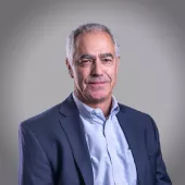
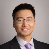
Vice President, Architecture, Advanced Design and Customer Enabling, Technology Development
Intel
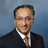
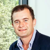
Richard Simoncic
Chief Operating Officer
Microchip Technology
Nasser Peyghambarian, PhD
Professor of Optical Sciences and Materials Science and Engineering
University of Arizona
Executive Panel Discussion: Investing in the Future—Capturing Long Range Goals
The winning strategy will continue to require accelerated investments in R&D, creating new labs and testing capabilities, advanced packaging pilot lines, next-gen university research facilities, and sustainable infrastructure. Arizona is positioned to attract investments and to remain a market leader in 2026, 2030, and beyond.
SEMI Breakfast Forum Organized by SEMI Arizona Chapter
In-Person | Arizona Time
Arizona Breakfast Forum
In-Person | May 6, 2026
7:30AM–12:30PM Arizona Time
7:30 am - 12:30 pm
Off
Add to Calendar2026-05-06 07:30:002026-05-06 12:30:00SEMI Arizona Breakfast ForumSEMI Breakfast Forum Organized by SEMI Arizona ChapterIn-Person | Arizona TimeEdwards Vacuum 2411 E. Germann Rd. Chandler, AZ 95286 United StatesSEMI.org[email protected]America/Los_Angelespublic
America/Los_Angeles
2
DuPont Joins SEMI Foundation’s Semiconductor PRIDE Initiative as a Founding Member
WILMINGTON, Del., Dec. 18, 2024 – DuPont (NYSE: DD) today announced it has joined the SEMI Foundation’s Semiconductor PRIDE (Semiconductor Professionals for Respect, Inclusion, Diversity, and Equity) initiative as a Founding Member. Semiconductor PRIDE, which launched earlier this year, is a coalition of companies who are committed to advancing LGBTQ+ equity and inclusion in the semiconductor workforce.
The Semiconductor Industry Association (SIA) projects that 58% of new semiconductor manufacturing and design jobs in the U.S. risk going unfilled by 2030 (SIA, 2023). This potential talent gap, along with shifting demographics where one in five Generation Z adults in the U.S. identifies as LGBTQ+, highlights the need to reevaluate strategies for preparing the future workforce (Gallup, 2024). Semiconductor PRIDE is a new working group within the SEMI Foundation, the workforce development arm of SEMI, that aims to broaden workforce development efforts to advance LGBTQ+ inclusion.
“Joining Semiconductor PRIDE reaffirms our commitment to fostering an inclusive supportive environment for LGBTQ+ employees and allies,” said Devon Benedict, Integrated Operations Program Leader, DuPont, and Events and Partnerships Co-Chair for the DuPont Pride employee network. “This partnership promotes the attraction of LGBTQ+ talent in the semiconductor workforce and is a natural fit with our values.”
The DuPont Pride network was instrumental in having the company join the SEMI Foundation’s efforts. Established in 1991, DuPont Pride embodies the company’s longstanding commitment to promote an inclusive, diverse, and innovative work environment. This is reflected in the company achieving a perfect score on the Human Rights Campaign Foundation’s Corporate Equality Index, the foremost benchmark for corporate policies and practices related to LGBTQ+ workplace equality in the U.S.
In collaboration with industry partners, DuPont is committed to not only closing the talent gap in the semiconductor industry but also ensuring that every individual has the opportunity to thrive in an inclusive environment.
About SEMI
SEMI® is the global industry association connecting over 3,000 member companies and 1.5 million professionals worldwide across the semiconductor and electronics design and manufacturing supply chain. We accelerate member collaboration on solutions to top industry challenges through Advocacy, Workforce Development, Sustainability, Supply Chain Management and other programs. Our SEMICON® expositions and events, technology communities, standards and market intelligence help advance our members’ business growth and innovations in design, devices, equipment, materials, services and software, enabling smarter, faster, more secure electronics. Visit www.semi.org, contact a regional office, and connect with SEMI on LinkedIn and X to learn more.
About DuPont
DuPont (NYSE: DD) is a global innovation leader with technology-based materials and solutions that help transform industries and everyday life. Our employees apply diverse science and expertise to help customers advance their best ideas and deliver essential innovations in key markets including electronics, transportation, construction, water, healthcare and worker safety. More information about the company, its businesses and solutions can be found at www.dupont.com. Investors can access information included on the Investor Relations section of the website at investors.dupont.com.
Science Foundry innovates on the traditional MEMS foundry business in three key ways: robust Multi-Project Wafer (MPW) offerings, a custom Manufacturing Execution System (MES), and a modular approach to our manufacturing capabilities. Some of our MPW offerings have been around for decades, while others were designed to serve the rapidly growing brain-computer interface industry, but all of our offerings provide production quality manufacturing at a fraction of the cost of custom wafer runs. We designed our MES for flexibility, enabling a level of efficiency beyond traditional wafer fabrication facilities and empowering us to engage with customers earlier in their development. Ultimately, this unlocks bandwidth from our technical staff to focus on creative problem solving and faster iteration cycles. We are expanding into a new facility with a modular upgrading plan that will add new process capabilities and strategically scale for the right partners. Our adaptability is our greatest strength, not only meeting our customers' needs but proactively anticipating the needs of nascent and burgeoning industries.
Kara Zappitelli, Foundry Director
Dr. Kara Zappitelli is the Lead Engineer & Foundry Director at Science Corporation’s pure-play MEMS foundry in RTP, North Carolina. She is a physicist-gone-engineer with a penchant for hard problems and more than a decade of experience in micro and nano fabrication for applications in neural engineering and MEMS. Kara joined Science at its inception and helped drive the initial R&D for the Science Eye device before moving to head up production of both internal and external devices. Kara received a B.S. in Physics from California Polytechnic State University in San Luis Obispo and a Ph.D. in Physics from the University of Oregon, where she was fabricating high surface area electrodes for applications in retinal prostheses. Before joining Science, she completed a post-doc investigating 2-photon lithography integration with 2D planar processing for complex neural interfaces.
Scott Smyser, VP of Sales
Scott has over 25 years of experience in the semiconductor industry leading commercial teams as a strategy, corporate marketing, and sales and business development professional. He has spent much of his career working with MEMS based products including timing devices, inertial sensors, and spectral sensors. At Science Foundry, Scott leads the go-to-market strategy developing long-term relationships with companies that need MEMS foundry services. Scott earned a BS in Electrical Engineering and an MBA from the University of Southern California.
United States
MSIG
8:00 am - 9:00 am
Off
Add to Calendar2025-02-12 08:00:002025-02-12 09:00:00Innovating in the MEMS Foundry BusinessUnited StatesSEMI.org[email protected]America/Los_AngelespublicRegister
NOTE: This webinar has been indefinitely postponed.
The FDA’s Center for Devices and Radiological Health (CDRH) launched the voluntary Total Product Life Cycle (TPLC) Advisory Program (TAP) Pilot to help spur more rapid development of high-quality, safe, effective, and innovative medical devices that are critical to public health. TAP’s primary goal is to expedite patient access to innovative medical devices by providing early, frequent, and strategic communications with the FDA and by facilitating engagement with other key parties for developers of devices of public health importance. To achieve this goal, a dedicated cadre of FDA TAP Advisors proactively provide solutions-focused engagement that is tailored to each TAP Innovator’s needs in advancing devices to market and patient access. In this seminar, FDA TAP Advisors will discuss this pilot program and provide participants input on when in their regulatory journey TAP may be an option for them.
ABOUT THE SPEAKERS:
Kimberly Knish, MS, CCRP, RAC Kimberly is a TAP Advisor within FDA’s Center for Devices and Radiological Health, Total Product Life Cycle (TPLC) Advisory Program (TAP). In this role, she establishes and cultivates a wide network of synergistic relationships across the entire medical technology innovation ecosystem and integrates ecosystem, sponsor, and lead reviewer input into strategic planning options intended to reduce stakeholder risk and maximize the opportunities of timely commercial rollout and sustainable patient access. She brings to the FDA 30 years of medical technology industry experience within clinical affairs, regulatory affairs, health economics, reimbursement and quality systems. She has been involved with all phases of medical device development (concept through obsolescence) involving device types from Class III implantables to wearables and remote monitors. Therapeutic expertise spans cardiovascular, nervous, digestive, endocrine, respiratory, and skeletal systems. Kimberly holds a B.A. degree in Biology from the College of St. Benedict, a M.S. degree in Management from Cardinal Stritch University and has professional certifications in clinical research (CCRP) and regulatory affairs (RAC).
April Marrone, PhD, MBA April is a Senior Advisor in the FDA/CDRH Total Product Lifecycle Program (TAP) since November 2023. Prior to her current role, April has served on the Obesity and Hepatobiliary Devices Team as the acting Assistant Director, Team Lead, Lead Reviewer, and chemistry consultant since 2014. In addition to supervisory, leadership, and medical device review responsibilities, April has promoted improvement in product manufacturing and quality through developing device specific FDA guidance documents, creating review tools to ensure consistency and quality in device review, and publishing external manuscripts on topics relevant to the FDA and industry on topics in the obesity and hepatobiliary device space. April has served as a Commissioner Fellowship Program (CFP) preceptor, mentor to new reviewers and advisors, and has developed and instructed Reviewer Certification Program courses.
Prior to joining CDRH in 2014, April was a Commissioner Fellow at FDA’s National Center for Toxicology Research (NCTR) and has served on the CFP Advisory Board. During her tenure at the NCTR, April did research to develop novel epigenetic approaches to safely assess the safety and carcinogenicity of FDA regulated products. Prior to joining the FDA, April was a post-doctoral scientist at the University of Pittsburgh, Children’s Hospital of Pittsburgh where she studied epigenetic regulation of congenital kidney disease in a mouse model. April also completed post-doctoral training at the Max Planck Institute for Biophysical Chemistry where she studied genetic and epigenetic regulation of neuromuscular disease. April has a PhD in Chemistry and BS in Physics from the University of Central Florida and an MBA from Florida Institute of Technology.
Plan now to join fellow semiconductor industry professionals at SEMI Headquarters in Milpitas, California at the 2025 SEMI EHS Summit.
Industry experts will present on the regulatory matters that will impact the industry in 2025 and beyond, followed by discussions on taking collective action to strengthen semiconductor manufacturing.
Topics will include:
US Regulatory Landscape under second Trump Administration and global impact
US EPA New Chemical Authorization Process
Europe: PFAS restriction, F-Gas restriction, GENESIS Consortium, REACH restriction, etc.
US EPA Technology Transition Rule
UN Plastics Treaty and related policies
US EPA TSCA New Substances of Concern
PFAS taxonomy
Overview of SEMI EHS activities, including SEMI PFAS Initiative
Attend, network and strategically prepare your company. This is an in-person event only.
EHS Summit 2025
Regulations, Rules, Allocations & Proposals
8:30 am - 3:30 pm
Off
Add to Calendar2025-02-11 08:30:002025-02-11 15:30:002025 EHS SummitPlan now to join fellow semiconductor industry professionals at SEMI Headquarters in Milpitas, California at the 2025 SEMI EHS Summit.Industry experts will present on the regulatory matters that will impact the industry in 2025 and beyond, followed by discussions on taking collective action to strengthen semiconductor manufacturing. Topics will include:US Regulatory Landscape under second Trump Administration and global impactUS EPA New Chemical Authorization ProcessEurope: PFAS restriction, F-Gas restriction, GENESIS Consortium, REACH restriction, etc.US EPA Technology Transition RuleUN Plastics Treaty and related policiesUS EPA TSCA New Substances of ConcernPFAS taxonomyOverview of SEMI EHS activities, including SEMI PFAS Initiative Attend, network and strategically prepare your company. This is an in-person event only.SEMI 673 South Milpitas Avenue Milpitas, CA 95035 United StatesSEMI.org[email protected]America/Los_Angelespublic
America/Los_Angeles
SEMICON Japan 2024 Opens Tomorrow to Highlight Smart Applications Powered by Semiconductor Technology
TOKYO – December 10, 2024 – SEMICON Japan, the region’s premier microelectronics industry conference and exhibition, opens tomorrow at Tokyo Big Sight. With more than 1,000 exhibitors from 35 regions, the conference gathers leaders from across the microelectronics manufacturing supply chain from December 11-13. SEMICON Japan 2024 will spotlight smart semiconductor applications for automotive, Internet of Things (IoT), and more, emphasizing industry insights, trends, and innovations that are powering the next wave of digital transformation. Registration is open.
Themed Strong Together, this year’s SEMICON Japan will feature two new events, including the Advanced Design Innovation Summit (ADIS) that will detail the future of semiconductor design and verification. Additionally, the inaugural SEMI Global Standards Summit will look at future advancements of semiconductor manufacturing and industry standardization strategies focusing on three important themes: Smart Manufacturing for Future Factories, Packaging Architectures & Materials, and Environmental Sustainability.
“Japan’s focus on worldwide semiconductor industry collaboration and its critical role in the broader supply chain solidify it as a key region for innovation,” said Jim Hamajima, President of SEMI Japan. “SEMICON Japan will expand opportunities to connect with leaders across the global industry to further accelerate the pace of technological developments in growing sectors such as AI, automotive, IoT, 5G, and more. As the world becomes increasingly digital, SEMICON Japan is bringing the industry together to drive the next wave of groundbreaking technology.”
Notable speakers at the SuperTHEATER, SEMICON Japan’s biggest stage, will include:
Akira Amari: Former Member of the House of Representatives Honorary Chairman, Diet Members Caucus for the Promotion of Semiconductor Strategy
Tetsuro Higashi: Chairperson of the Board, Rapidus Chairman, Leading-Edge Semiconductor Technology Center
Dario Gil: Senior Vice President and Director of IBM Research, IBM
Ho-Young Son: Vice President of Advanced Package Development, SK hynix
Terushi Shimizu: Representative Director, President and CEO, Sony Semiconductor Solutions
Concurrent Events with SEMICON Japan
Advanced Packaging and Chiplet Summit (APCS): This summit will include an exhibition area for technologies that support 2.5D, 3D, redistribution layers, through silicon vias, chiplets, and more. APCS will also feature networking opportunities and conference sessions led by the world’s top industry players.
FLEX Japan: This event will bring device and material suppliers together with vendors who provide the final products, with the goal of creating new business opportunities within the flexible device and printed electronics sectors.
Other SEMICON Japan Highlights
Workforce Development Programs*:SEMICON Japan’s workforce development programs will include Mirai College at SEMICON*, where 51 semiconductor-related companies will gather to help attendees learn about the industry. In addition, 70 universities* from across Japan will share their latest research and provide collaboration opportunities for those in academia*.
Technology Pavilions:The many technology pavilions at SEMICON Japan include the Quantum Computing, Ministry of the Environment, Power Electronics, Clean Room, and SEMI Sustainability HUB pavilions. Each pavilion will feature targeted exhibitions related to their focus area.
Interactive Attractions:To help encourage semiconductor industry interest among the younger generation, SEMICON Japan will feature Yoichi Ochiai’s Passion Lab, an initeractive discussion led by media artist, Yoichi Ochiai. In addition, SEMICON STADIUM will allow attendees to see, touch, and experience semiconductors through sports-playing AI robots, such as AI basketball robot “CUE6” (Toyota Motor Corporation), table tennis robot “Forpheus” (Omron), baseball swing analysis using Fujitsu Human Motion Analytics (Fujitsu), and the fastest robot to solve a puzzle cube “TOKUFASTbot” (Mitsubishi Electric).
SEMI® is the global industry association connecting over 3,000 member companies and 1.5 million professionals worldwide across the semiconductor and electronics design and manufacturing supply chain. We accelerate member collaboration on solutions to top industry challenges through Advocacy, Workforce Development, Sustainability, Supply Chain Management and other programs. Our SEMICON® expositions and events, technology communities, standards and market intelligence help advance our members’ business growth and innovations in design, devices, equipment, materials, services and software, enabling smarter, faster, more secure electronics. Visit www.semi.org, contact a regional office, and connect with SEMI on LinkedIn and X to learn more.
Contact Information:
Association Contacts
Shuichi Sato/SEMI Japan Phone: 81.3.3222.5757 Email: [email protected]
Siemens extends Veloce hardware-assisted verification and validation with new Innexis shift-left software
Innexis delivers a set of products and capabilities to address demand for shift-left software development in the IC development process
With more demanding software workloads, it is critical to facilitate the development and execution of realistic workloads early in the design phase to shorten overall development time and identify hardware and software defects earlier
Siemens Digital Industries Software announced today the Innexis product suite, a complement to its industry leading Veloce™ hardware-assisted verification and validation system.
Building on the success and rapid adoption of Veloce, Siemens’ Innexis product suite delivers a set of capabilities to address customer demand for shift-left software in the early phases of IC development. These products include a hardware/software development flow from virtual to hybrid to full RTL, an architecture native virtual platform for early high-speed software development and a simulation backplane that enables the development of digital twins in Siemens’ PAVE360™ software for software-defined vehicles and other complex systems.
“The complexity of integrated circuits (IC) is increasing exponentially, designers need more efficient methodologies to meet industry demands. Veloce has seen rapid adoption by industry leaders to help solve this critical bottleneck. The Innexis product suite extends workflow improvements from Veloce to help our customers shift left their IC development and debug cycle,” said Jean-Marie Brunet, vice president and general manager, Hardware-Assisted Verification, Siemens Digital Industries Software. “This enables IC design to begin months before final RTL, all while using a common software workload across the development process.”
Adoption of a shift-left approach for software development and IP verification processes is now mandatory. As chip designs become increasingly complex due to more demanding software workloads, it is critical to enable the development and execution of realistic workloads early in the design phase. A proactive shift-left software approach helps mitigate the risk of identifying issues late in the development cycle.
“The implementation of Innexis in our development process has significantly enhanced software and system validation performance, thereby improving the efficiency of our teams and projects. By enabling heterogeneous component modeling within virtual platforms, it allows us to create realistic high-speed models of System on Chips (SoCs),” said Ari Hautala, Principal System Architect, Nokia Mobile Networks. “Furthermore, the integration of these high-speed virtual platforms with RTL IP on Veloce emulators facilitates superior overall performance while still permitting precise cycle-accurate performance and power analysis on RTL model components. Additionally, Innexis offers exceptional visibility and debuggability for the SoC design, along with the capability to integrate and execute a large number of complex test cases effectively.”
Currently, the Innexis product suite consists of:
Innexis Developer Pro: Innexis Developer Pro software provides a connected development flow from virtual to hybrid to full RTL. This provides a comprehensive environment for accelerating the creation of complex SoC design supporting a wide range of use-cases including seamless hardware-software co-development, co-validation, and pre-silicon cycle accurate analysis and validation. Innexis Developer Pro supports the modelling of complex SoC’s with heterogeneous cores and custom SystemC model components. In addition, it provides the ability to run in both virtual plus RTL hybrid mode for high performance execution, and then at a time of interest switch to full RTL emulation enabling high accuracy analysis of the full SoC when required.
Innexis Architecture Native Acceleration (ANA): Innexis Architecture Native Acceleration software is a cloud- based high-speed virtual platform. By running natively on Arm based servers the software workloads run at much higher speeds than on typical instruction set simulation based virtual platforms. Cloud hosting also provides scalable compute resources and simple browser-based access and tools. Innexis Architecture Native Acceleration can also run on local Arm based servers if preferred. In both cases it enables early software development and testing, and early software defect identification.
Innexis Virtual System Interconnect: Innexis Virtual System Interconnect software facilitates the creation and simulation of comprehensive system level digital twin platforms by seamlessly connecting multi-behavioral virtual and physical subsystems, supporting a variety of communication protocols. Innexis Virtual System Interconnect behavioral models can include Innexis Developer Pro or Innexis Architecture Native Acceleration SoC models, supporting system-level shift-left software development and RTL verification.
To learn more about Siemens’ Innexis product suite and how it addresses the demand for shift-left software development in the integrated circuit development process, visit: www.siemens.com/innexis
About Siemens
Siemens Digital Industries Software helps organizations of all sizes digitally transform using software, hardware and services from the Siemens Xcelerator business platform. Siemens' software and the comprehensive digital twin enable companies to optimize their design, engineering and manufacturing processes to turn today's ideas into the sustainable products of the future. From chips to entire systems, from product to process, across all industries. Siemens Digital Industries Software – Accelerating transformation.
Note: A list of relevant Siemens trademarks can be found here. Other trademarks belong to their respective owners.
Heidelberg Instruments Reports Major Orders for the VPG+ 1400 FPD Volume Pattern Generator from Leading Asian Photomask Manufacturers
Heidelberg Instruments Reports Major Orders for the VPG+ 1400 FPD Volume Pattern Generator from Leading Asian Photomask Manufacturers
Heidelberg, Germany – Heidelberg Instruments has secured two major orders for its VPG+ 1400 FPD Volume Pattern Generator from leading photomask manufacturers in Asia, with a total order value between EUR 9 million and EUR 10 million. Deliveries are scheduled for 2025.
“These significant order intakes mark major milestones for the company, reinforcing our market position and driving further innovation and growth in the display technology sector”, says Alexander Forozan, VP of Global Sales and Business Development.
The VPG+ 1400 is Heidelberg Instruments’ largest system, specifically designed for large-format photomask patterning in the flat panel display (FPD) industry. It supports mask sizes up to 1400 x 1400 mm², making it ideal for various flat panel display generations (G4 to G8). The VPG+ 1400 sets a new standard for high-throughput photomask production, offering the precision and scalability required for large displays. Additionally, it delivers the accuracy needed to produce large-area halftone photomasks for flat panel displays.
Equipped with advanced metrology and alignment features, including Cognex AI-based image recognition, the system ensures precise alignment for multilayered masks. Its linear and nonlinear coordinate corrections further enable precise overlay across tools.
By addressing the diverse exposure needs of customers, Heidelberg Instruments' large-area VPG+ Volume Pattern Generators have proven to be valuable assets in display photomask production lines.
From Concept to Reality: Advancing Digital Twin in Semiconductor Manufacturing
This event is now sold out. Please register if you'd like to receive access to presentation materials.
SEMI Member: $225
Non-Members: $295
Cancellations received on or before November 17, 2023 will be fully refunded. After this date, only substitutions will be accepted.
Please email your cancellation request to Agnes Cobar at [email protected]. Refunds will not be issued for cancellations (including no-shows) made after November 17th, 2023.
Substitutes are only accepted with written permission from the original registrant.
Digital Twin technology has gained significant traction in a variety of industries and is now in its early stages of adoption by the semiconductor industry. In this workshop, we will hear from across the ecosystem (OEMs, Platforms, end users, and more) as to the various levels of Digital Twins needed, the development challenges, opportunities, and recommendations. The development of full tool or full-process level semiconductor digital twins is challenging but has the potential to significantly improve the productivity & quality of operations.
Primarily beneficial for developers, and end-users of DT’s to attend so that we can understand the challenges, and scope of development effort required to create and deploy such DT systems in manufacturing.
Hosted by the SEMI Smart Manufacturing Initiative.
SEMI HQ 673 S Milpitas Blvd. Milpitas, CA95035 United States
Morning, Day 1: December 4, 2024
8:00 am
-
12:20 pm
Equipment Level Digital Twins (Equipment Makers)
Digital twins from equipment makers are virtual replicas of their physical products. They are created using data collected from sensors on the equipment, as well as from design and engineering drawings.
8:00 am
-
9:00 am
Registration & Breakfast
9:00 am
-
9:15 am
Mark Da Silva
SEMI
Welcome All
9:15 am
-
9:40 am
Supika Mashiro
Sr. Expert/TEL, Co-chair of the IRDS Factory Integration IFT (Focus Team)
TEL
Emergence of Digital Twin technology in the IRDS Factory Integration focus roadmap
9:40 am
-
10:05 am
Ala Moradien
Director, CAE Programs and Digital Twin Initiatives
Applied Materials
AppliedTwin™: A Digital Twin Platform for Semiconductor Manufacturing, Use Case in Sustainability
10:05 am
-
10:30 am
Joe Ervin
Senior Director and Product Line Head, Semiverse™ Solutions
Lam Research
A Single Digital Twin for Semiconductor Manufacturing? Semiverse™ Solutions and Building the Digital Family
10:30 am
-
10:45 am
Coffee Break
10:45 am
-
11:10 am
Sean Glazier
Software Engineer IV
Onto Innovation
Building a digital twin model is EASY. Getting the model deployed and used every day, now that’s the challenge
11:10 am
-
11:35 am
Basil Milton
Senior Manager, Ball Bonder Process R&D
Kulicke & Soffa
Digital Twin Improvements for Wire Bond Process Optimization
11:35 am
-
12:20 pm
Moderator
Mark Huntington
McKinsey
Open Forum/Panel/Breakout
12:20 pm
-
1:30 pm
Lunch
Afternoon, Day 1: December 4, 2024
1:30 pm
-
5:00 pm
Chamber Process, Operations & Planning Level Digital Twin (Solution Providers)
Solution providers offer a variety of products and services to help companies implement and manage digital twins (physics-based process models for components or sub-systems).
1:30 pm
-
1:55 pm
Sarbajit Ghosal
Lead Research Engineer
SC Solutions, Inc.
Fast, Physics-based Models for Real-time Process Control And Monitoring
1:55 pm
-
2:20 pm
Norman Chang
Ansys/IEEE Fellow and Chief Technologist of Electronics, Semiconductor, and Optics BU
Ansys Inc.
Enabling ML-augmented Digital Twin for Semiconductor Manufacturing
2:20 pm
-
2:45 pm
Holland Smith
Director of Technical Marketing, INFICON IMS (Intelligent Manufacturing Systems)
INFICON
The Operations Digital Twin: Why Every Factory Needs One, and Why Many Don't Have One (Yet)
2:45 pm
-
3:00 pm
Coffee Break
3:00 pm
-
3:25 pm
Chandra Reddy
Senior Technical Staff Member, AI Applications
IBM Research
Generative AI enabled Digital Twins
3:25 pm
-
3:50 pm
Jon Herlocker
Founder & CEO
Tignis
Practical Machine Learning Applications for the Process Modelling and Optimization of Manufacturing Process Tools and Process Lines
3:50 pm
-
4:15 pm
Ken Smerz
CEO
Zelus
Digital Twin Creation and Application
4:15 pm
-
5:00 pm
Moderator
John Behnke
GM FPS Product Line
INFICON
Open Forum/Panel/Breakout
5:00 pm
-
7:00 pm
Networking Reception
Morning, Day 2: December 5, 2024
8:00 am
-
12:20 pm
DT Adoption & Implementation (Device Makers)
As a device maker, a digital twin is a critical tool for improving productivity, quality, and efficiency. A digital twin is a virtual representation of your physical devices or fab, and it can be used to simulate and optimize operations.
8:00 am
-
9:00 am
Breakfast
9:00 am
-
9:05 am
Mark Da Silva
SEMI
Day 2 - Welcome
9:05 am
-
9:30 am
Prof. Phillip Wong
Professor of Electrical Engineering, Willard R. and Inez Kerr Bell Professor in the School of Engineering Stanford University
Stanford
A Vision for the Future Semiconductor Fab
9:30 am
-
9:55 am
Steven J Meyer
General Manager and Sr. Principal Engineer, Advanced Industrial Systems
Intel Corporation
High Value from Digital Twins in Semiconductor Manufacturing
9:55 am
-
10:20 am
Jae Y. Park
VP of Technology
Samsung
AI Powered Digital Twin: Transforming Smart Manufacturing
10:20 am
-
10:45 am
Coffee Break
10:45 am
-
11:10 am
Rosa Javadi
Principal Engineer
Jabil
Smart Manufacturing Technology for Complex Integrated Systems
11:10 am
-
11:35 am
Amit Lal
Professor
Cornell University
Peter Doerschuk
Professor
Cornell University
Ben Davaji
Assistant Professor
Northeastern University
Digital Twin Frameworks for an Academic Research and Development Cleanroom
11:35 am
-
12:20 pm
Moderator
Bobby Mitra
Deloitte
Open Forum/Panel Discussion - Developing Full Process Level Digital Twin – Challenges
12:20 pm
-
1:30 pm
Lunch
Afternoon, Day 2: December 5, 2024
1:30 pm
-
5:00 pm
DT Connectivity and Platform Integration (Cloud, Facilities, & Supply Chain)
Solution providers offer a variety of products and services to help companies implement and manage digital twins including integration, connectivity, & security including horizontal integration across the supply chain.
1:30 pm
-
1:55 pm
Rad Desiraju
Director , WW Industry Advisory
Microsoft
Unlocking Innovation with Digital Twins
1:55 pm
-
2:20 pm
Gautham Unni
Head of Solutions & Business Development (Semiconductor)
AWS
Accelerate your Digital Twin journey with AWS
2:20 pm
-
2:45 pm
David Gross
Portfolio Development Executive, Manufacturing Digitalization, Semiconductor Industry
Siemens
Srividya Jayaram
Principal Product Engineering ManagerSiemens EDA
Siemens EDA
Siemens: Accelerating technology From Design to HVM
2:45 pm
-
3:00 pm
Coffee Break
3:00 pm
-
3:25 pm
Slava Libman
CEO
FTD Solutions INC
Digital Twins Enabling Environmental Sustainability
3:25 pm
-
3:50 pm
Becky Kelderman
Manager
Rockwell Automation
The Nimble Supply Chain with Digital Twin
3:50 pm
-
4:15 pm
Ram Walvekar
VP and PLM Head, Digital Transformation Unit
HCL Technologies
Integrated Cognitive Digital Twin for Semiconductor Equipment
4:15 pm
-
5:00 pm
Paul Trio - Moderator
SEMI
Required Standards for Digital Twin Technology - Open Forum/Panel/Breakout
-
Join us for a 2-day deep dive into the expanding world of Digital Twin (DT) technology in the semiconductor realm. Understand its potential challenges and opportunities, and discover its transformative power in enhancing operational productivity and quality. Calling all DT developers and end-users: collaborate, learn, and pave the way for DT's integration into manufacturing!
This event is now sold out. Please register if you'd like to receive notifications about available spaces or access to presentation materials.
From Concept to Reality: Advancing Digital Twin in Semiconductor Manufacturing
[IN-PERSON EVENT]
December 4-5, 2024
8:00 AM – 5:00 PM PT
8:00 am - 5:00 pm
Off
Add to Calendar2024-12-04 08:00:002024-12-05 17:00:00From Concept to Reality: Advancing Digital Twin in Semiconductor ManufacturingJoin us for a 2-day deep dive into the expanding world of Digital Twin (DT) technology in the semiconductor realm. Understand its potential challenges and opportunities, and discover its transformative power in enhancing operational productivity and quality. Calling all DT developers and end-users: collaborate, learn, and pave the way for DT's integration into manufacturing!
This event is now sold out. Please register if you'd like to receive notifications about available spaces or access to presentation materials.SEMI HQ 673 S Milpitas Blvd. Milpitas, CA 95035 United StatesSEMI.org[email protected]America/Los_Angelespublic
America/Los_Angeles
On-demand
2025 Technology Workshops Shaping the Future of Electronics
Registration
Early Bird Pricing (until March 25, 2025) $375 members $525 non-members
Regular Pricing (After March 25, 2025) $525 members $699 non-members
MDM2 members please contact Michelle Fabiano, [email protected], for discount information.
Complimentary student registration is available but has limited capacity. Students can Register here to be contacted about complimentary attendance after March 15th.
Cancellation Policy
Cancellations received on or before March 25, 2025, are fully refunded with a $50 processing fee. Refunds will not be issued for cancellations (including no-shows) made after March 25, 2025, and only substitutions are accepted with a written note from the registered attendee. Please email your cancellations or substitutions on company letterhead to Michelle Fabiano at [email protected].
Industry Tours Take advantage of an exclusive industry tour at Medtronic on April 21, just before our workshop begins! Please note that space is limited and transportation will not be provided. Don't miss this unique opportunity!
Shaping the Future of Flexible Hybrid Electronics: FHE Technical Gap Analysis workshop Join us on April 22 for a focused technical gap analysis workshop on Flexible Hybrid Electronics (FHE) to shape FlexTech’s 2025 Request for Proposals (RFP). With a history of over five dozen R&D projects, FlexTech has driven advancements in flexible batteries, energy harvesting, and system integration. Hear from principal investigators on the latest developments and join breakout sessions to explore challenges, gaps, and priorities for future innovation with industry, government, and academic leaders.
Why Attend: Contribute to FlexTech’s 2025 priorities, learn about cutting-edge developments, and Join breakout sessions and network with key experts.
The day will conclude with a Mayo Clinic Lab for function tour followed by a Student Poster Networking Reception.
Advancing Human Performance Technologies: NBMC Technical Gap Analysis Workshop Join us on April 23 for the Nano-Bio Materials Consortium (NBMC) Technical Gap Analysis Workshop, a focused forum on wearables and bio-signal sensing technologies for real-time cognitive and physical state monitoring, augmentation, and intervention. Participants will address critical technical gaps in preparation for the next NBMC Request for Proposal.
NBMC brings together industry, government, and academia to advance early-stage nano and bio technologies, driving innovations in low-cost wearable sensors and communication systems through over three dozen R&D projects.
The day will conclude at the Phoenix Bioscience Core, located in the heart of the innovator's district in downtown Phoenix, Attendees will enjoy guided tours, a reception and a keynote presentation on "Bridging Clinical Needs and Emerging Technology: Emerging Device-Based Health Intervention Platforms: Wearables, Robotics, and BioHybrids." Networking opportunities will be available throughout these activities.
Clinician Insights Shaping the Future of Electronics: MDM2 and Smart MedTech Forum Join us on April 24, for an inspiring and dynamic session spotlighting the collaboration between MDM2 (Medical Device Manufacturing Multiplier ) and the Smart MedTech Initiative. This forum highlights the critical role of clinician and patient perspectives in driving innovation for next-generation medical devices.
Together, MDM2—a consortium dedicated to positioning Greater Phoenix as a leading hub for digital medical device manufacturing—and SEMI Smart MedTech Initiative are working to bridge the gap between emerging technologies and real-world needs. Discussions will explore how clinician insights can spark innovation in medical devices, accelerate technology adoption and commercialization and leverage AI and machine learning to advance manufacturing processes.
An evening event will be hosted by Venture Cafe at the end of the workshop to engage with the local innovation community.
Including with registration are breakfasts, breaks, lunches and receptions.
ASU Health Futures Center 6161 E Mayo Blvd Phoenix, AZ85054 United States
Monday, April 21 (Medtronic Tour)
2:00 pm
Medtronic Tour
(Tour sold out. Sign up for the waitlist.)
Join us for an exclusive one-hour tour of Medtronic’s facility, to explore its advanced operations in designing and manufacturing microelectronics for implantable medical devices.
Attendees will break into groups for smaller discussions to identify challenges, prioritize those challenges and identify opportunities on critical issues discussed throughout the morning session.
3:05 pm
-
3:20 pm
Break
3:20 pm
-
4:10 pm
Breakout Sessions Readout
4:30 pm
-
6:00 pm
Student Poster Networking Reception & Mayo Clinic Lab for Function Tour
Mayo Clinic
IERB Building
5951 E. Mayo Blvd
Phoenix, AZ 85054
Mayo Lab Tour: If you're interested, please sign up at the registration desk. Space is limited to 20 participants and will be available on a first-come, first-served basis.
Note: Transportation to this reception will not be provided. (2 minute drive.)
Attendees will break into groups for smaller discussions to identify challenges, prioritize those challenges and identify opportunities on critical issues discussed throughout the morning session.
3:05 pm
-
3:20 pm
Break
3:20 pm
-
4:10 pm
Breakout Sessions Readout
5:00 pm
-
7:00 pm
Networking Reception and Tours of Wexford Connect
Enjoy Networking, concurrent tours, and presentation content
850 Phoenix Bioscience Core
850 N 5th Street
Phoenix, AZ 85004 https://850pbc.com
5:00 pm - 5:30 pm: Tours of Wexford Connect (Limited to 30 people)
6:15 pm - 7:00 pm: Panel Discussion:
Bridging Clinical Needs and Emerging Technology: Research, Implementation, and Scale. Moderator: Chris Yoo, General Partner, Xcellerant Ventures Panelists: Suman Bose, Assistant Professor of Biomedical Engineering, Mayo Clinic Hakan Ceylan, Assistant Professor and Principal Investigator, Mayo Clinic Ross Bundy, CEO, CRISPRQC Elsa Abruzzo, CEO, Anuncia Medical Allen Waziri, CEO and Co-Founder, iCE Neurosystems
Note: Transportation will not be provided. (30+ minute drive.)
Panel Discussion: The Arizona MDM2 Consortium - Investing in the Medical Technology Manufacturing Renaissance
Moderator: Chris Yoo, Founder and CEO and Regional Innovation Officer, MDM2 Consortium Panelists: Kiran Avancha, Chief Innovation Officer, HonorHealth Rochelle Rivas, District Director for Healthcare Innovation, Maricopa Community Colleges Alex Tessmer, Associate Director, BD Peripheral Intervention, Ideation
9:45 am
-
10:10 am
Jonathon Parker
Neurosurgeon, Director of Device-Based Neuroelectronics Lab
Mayo Clinic, Arizona
Aman Verma
Hospitalist
Mayo Clinic, Arizona
FIRESIDE CHAT: How can wearables and implantables improve care of the acutely ill patient?
Moderator: Jonathon Parker , Neurosurgeon, Director of Device-Based Neuroelectronics Lab, Mayo Clinic - Arizona Participants: Aman Verma, Hospitalist, Mayo Clinic, Arizona
10:10 am
-
10:25 am
Break
10:25 am
-
11:10 am
Moderator
Kiran Avancha
Chief Innovation Officer
Honor Health Innovations
Craig Norquist
Chief Innovation Officer
Honor Health
Matthew Anderson
Chief Medical Information Officer - Ambulatory
Honor Health
PANEL DISCUSSION: Health Data 2035: How do we Capture, Integrate, and Secure Health Data Streams From Wearables and Implantables to Improve Patient Care?
Moderator: Kiran Avancha, Chief Innovation Officer, Honor Health Innovations Panelists: Craig Norquist, Chief Innovation Officer, Honor Health Matthew Anderson, Chief Medical Information Officer - Ambulatory, Honor Health
11:10 am
-
11:45 am
Jonathon Parker
Neurosurgeon, Director of Device-Based Neuroelectronics Lab
Mayo Clinic, Arizona
Bart M. Demaerschalk
Vascular Neurologist
Mayo Clinic, Arizona
Chandan Krishna
Neuro-endovascular Neurosurgeon
Mayo Clinic - Arizona
FIRESIDE CHAT: Stroke Care 2035- How Can Digital Health Data Transform Stroke Care?
Moderator: Jonathon Parker , Neurosurgeon, Director of Device-Based Neuroelectronics Lab, Mayo Clinic - Arizona Participants: Bart M. Demaerschalk, Vascular Neurologist, Mayo Clinic, Arizona Chandan Krishna, Neuro-endovascular Neurosurgeon, Mayo Clinic, Arizona
11:45 am
-
12:15 pm
Jonathon Parker
Neurosurgeon, Director of Device-Based Neuroelectronics Lab
Mayo Clinic, Arizona
Nandita Khera
Oncologist, Associate Chair of Digital Health
Mayo Clinic
FIRESIDE CHAT: Real-Time Oncology - How Can Wearables and Implantables Reshape Oncology Care in 2035?
Moderator: Jonathon Parker , Neurosurgeon, Director of Device-Based Neuroelectronics Lab, Mayo Clinic - Arizona Participants: Nandita Khera, Oncologist, Associate Chair of Digital Health, Mayo Clinic
12:15 pm
-
1:00 pm
Moderator
Randal Schulhauser
Founder and CEO
Schulhauser Associates LLC
Jonathon Parker
Neurosurgeon, Director of Device-Based Neuroelectronics Lab
Mayo Clinic
Allen Waziri
Neurosurgeon, Co-Founder iCE Neurosystems
iCE Neurosystems
Paul Gerrish
VP, Technology and Medtronic Fellow
Medtronic
Panel Discussion: The New Frontier of Long-Term Brain Monitoring: Brain Computer Interface Re-Imagined
Moderator: Randal Schulhauser, Founder and CEO, Schulhauser Associates LLC Panelists: Jonathon Parker, Neurosurgeon, Director of Device-Based Neuroelectronics Lab, Mayo Clinic Allen Waziri, Neurosurgeon, Co-Founder iCE Neurosystems, iCE Neurosystems Paul Gerrish, VP, Technology and Medtronic Fellow, Medtronic
Division Director, Integrative Health and Performance Sciences
BlueHalo
Deon Chen
Sr. Manager, HEOR Strategic Planning
BD
Panel Discussion: Digital Health Revolution: Insights and Innovations
Moderator: Douglas Kiehl, BioCrossroads/Purdue Panelists: Bharath Rajagopalan , Director – Strategic Marketing, Health & Wellness, STMicroelectronics Anirban Bandyopadhyay, Senior Director, Global Foundries Stephaney Shanks, Division Director, Integrative Health and Performance Sciences, BlueHalo Deon Chen, Sr. Manager, HEOR Strategic Planning, BD
4:30 pm
-
7:00 pm
Evening Program Hosted by Venture Café
850 Phoenix Bioscience Core
850 N 5th Street
Phoenix, AZ 85004 https://venturecafephoenix.org/
Venture Café Phoenix is a dynamic weekly gathering where entrepreneurs, innovators, and business leaders connect to exchange ideas and build meaningful relationships.
Note: Transportation to this program will not be provided (30+minute drive)
5:40 pm
-
6:30 pm
Nandini Tandon
Co-Founder of Silicon Valley based VC in HealthTech
IndUS Setu Global Foundation
Jami Mei
VP of Business Development
Arizona Commerce Authority
Douglas E. Kiehl
Sr. Vice President
BioCrossroads
Mark Dydyk
Director of Engineering & Operations
Medtronic
Fireside Chat: Harnessing Semiconductor For transformational Advancements in HealthTech
Abstract Moderator: Nandini Tandon Panelists: Jami Mei, VP of Business Development, Arizona Commerce Authority Douglas E. Kiehl, Sr. Vice President, BioCrossroads Mark Dydyk, Director of Engineering & Operations, Medtronic
Join us for a three-day workshop uniting FlexTech, NBMC, Smart MedTech, and the Medical Device Manufacturing Multiplier (MDM2) — a consortium of companies, institutions, and statewide organizations working to establish Greater Phoenix as a premier hub for medical device manufacturing. This collaborative event will drive innovation in electronics and medical technologies by bringing together industry leaders, innovators, and stakeholders.
The workshop will delve into advancements, challenges, and gaps in critical technologies such as flexible hybrid electronics, hybrid electronics, and bio-signal sensing for real-time cognitive and physical state monitoring and augmentation and will highlight the collaboration between the Smart MedTech Initiative and MDM2, focusing on the voice of the customer—clinicians and patients.
2025 Technology Workshop Shaping the Future of Advancing Electronics and Medical Technologies
- FHE Gap Analysis and NBMC Gap Analysis
- MDM2 and Smart Medtech Workshop
8:00 am - 6:00 pm
Off
Add to Calendar2025-04-22 08:00:002025-04-24 18:00:002025 Technology Workshops Shaping the Future of ElectronicsPresented By
Join us for a three-day workshop uniting FlexTech, NBMC, Smart MedTech, and the Medical Device Manufacturing Multiplier (MDM2) — a consortium of companies, institutions, and statewide organizations working to establish Greater Phoenix as a premier hub for medical device manufacturing. This collaborative event will drive innovation in electronics and medical technologies by bringing together industry leaders, innovators, and stakeholders.The workshop will delve into advancements, challenges, and gaps in critical technologies such as flexible hybrid electronics, hybrid electronics, and bio-signal sensing for real-time cognitive and physical state monitoring and augmentation and will highlight the collaboration between the Smart MedTech Initiative and MDM2, focusing on the voice of the customer—clinicians and patients. ASU Health Futures Center 6161 E Mayo Blvd Phoenix, AZ 85054 United StatesSEMI.org[email protected]America/Phoenixpublic
America/Phoenix
Register Now