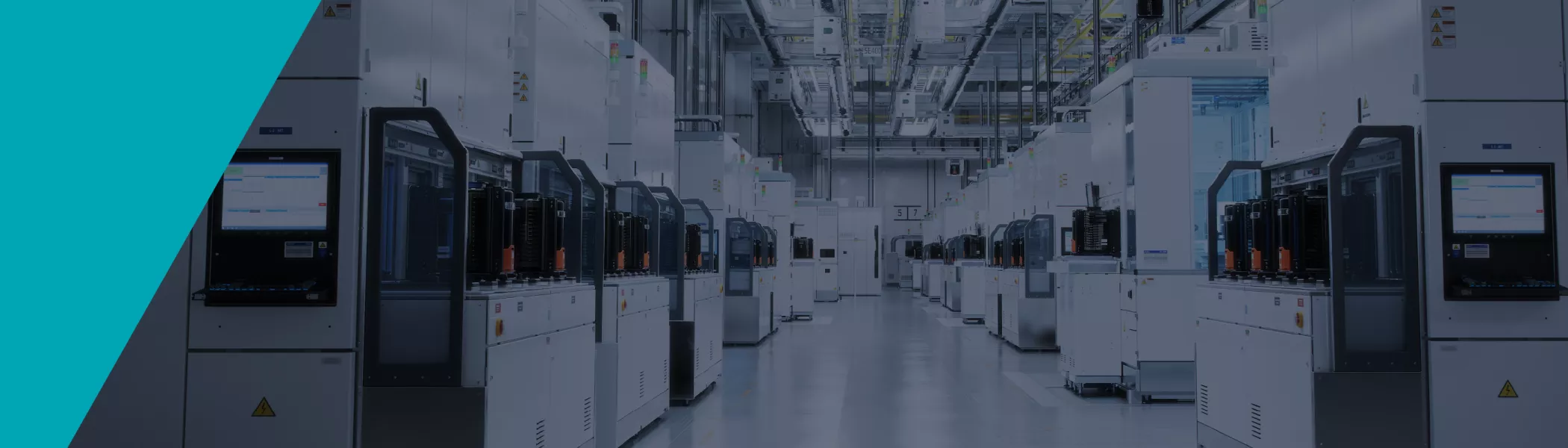
downloadGroupGroupnoun_press release_995423_000000 copyGroupnoun_Feed_96767_000000Group 19noun_pictures_1817522_000000Member company iconResource item iconStore item iconGroup 19Group 19noun_Photo_2085192_000000 Copynoun_presentation_2096081_000000Group 19Group Copy 7noun_webinar_692730_000000Path
Skip to main content
Default Banner Image

United States

Belgium France Germany Ireland Italy Japan Malaysia Singapore South Korea Taiwan United States Vietnam SEMI U Free Webinar Business Training Featured Speakers
Highlighted content

SEMI University celebrates its second-year anniversary! Our pledge remains unwavering: providing comprehensive, technical education to equip you with the skills needed for a prosperous journey in the semiconductor sector.

Are you ready to take your semiconductor industry knowledge to the next level? We're thrilled to invite you to our upcoming webinar titled "SEMI University - Overview and 2025 Roadmap." This webinar promises to be an informative session where you'll gain insights into the latest updates, exciting live trainings, new certifications, and courses offered by SEMI U in 2025.  

During this webinar, you can expect to:  

  • Discover the latest updates and enhancements to SEMI U's course catalog.  
  • Learn about the exciting live, in-person training courses scheduled for this year.  
  • Get insights into new courses designed to keep you ahead in the industry.  
  • Gain access to a special 10% discount on ALL on-demand courses.  

Choose your session:

United States

Headshot of Naresh Naik
Naresh Naik
Director, SEMI University
SEMI
SEMI U Workforce Development

Join us to discover our current course offerings, upcoming in-person and virtual trainings, and more! Engage in a Q&A session. Plus, by attending this free webinar, you'll receive a 10% discount code for all on-demand courses. Please scroll down below to "Choose Your Session" and register for the webinar time that works best for you! 

Off Add to Calendar 2025-05-15 00:00:00 2025-05-15 00:00:00 SEMI University - Overview & 2025 Roadmap Join us to discover our current course offerings, upcoming in-person and virtual trainings, and more! Engage in a Q&A session. Plus, by attending this free webinar, you'll receive a 10% discount code for all on-demand courses. Please scroll down below to "Choose Your Session" and register for the webinar time that works best for you!  United States SEMI.org [email protected] America/Los_Angeles public Register Now
Event format
Promote in calendar
Off
Belgium China France Germany Italy Japan Singapore South Korea Taiwan United States Register Now Handprint 800x800 Business Executive Featured Speakers
Highlighted content

United States

Mousumi black white
Dr. Mousumi Bhat
Vice President, Sustainability
SEMI
chris bw
Chris Jones, PhD
Env. Solutions Business Development Manager
Edwards
Ajay bw
Ajay Gupta, PhD
Postdoctoral Associate
MIT
Tiina Pajula
Tiina Pajula
Sr. Principal
AFRY Management Consulting
Greg BW
Dr. Gregory Norris
Director, Sustainability and Health Initiatives for NetPositive Enterprise
MIT
Marijn bw
Marijn Vervoorn
Director Sustainability Strategy
ASML
Sustainability

This webinar will feature the authors and analysts of the recently released report "Toward a Shared View on the Climate Impact of Digital Technology" exploring the positive climate impact of digital technology and how to calculate when understanding any organizations footprint. They will explain the role of the semiconductor industry, in particular, in shaping a more sustainable future and how to account for that in emissions calculations. Download the report here.

8:00 am - 9:00 am Off Add to Calendar 2025-03-25 08:00:00 2025-03-25 09:00:00 Quantifying the Positive Impacts of the ICT Sector This webinar will feature the authors and analysts of the recently released report "Toward a Shared View on the Climate Impact of Digital Technology" exploring the positive climate impact of digital technology and how to calculate when understanding any organizations footprint. They will explain the role of the semiconductor industry, in particular, in shaping a more sustainable future and how to account for that in emissions calculations. Download the report here. United States SEMI.org [email protected] America/Los_Angeles public America/Los_Angeles
Event format
United States Image Training

Course Description

The first part of the course provides a brief overview of semiconductor design and fabrication steps, encompassing IC design techniques, all wafer processing steps, assembly, and packaging. It delves into semiconductor jargon in laypeople terms, and various substrate types such as Si, SiGe, FDSOI, GaAs, SiC, GaN. Additionally, it discusses different types of transistors like pMOS, nMOS, Bipolar, BiCMOS, CMOS, FinFets, and GAA and their evolution and what applications they are used in.
 
The second part of the course focuses on semiconductor business aspects such as silicon economics, wafer processing costs, semiconductor revenue forecasts, driving forces in the industry, top semiconductor IDMs, market competitors based on market share, OEMs, foundries, top tool vendors, and Fabless companies.  Addresses the fastest-growing semiconductor markets based on geographic locations and applications, identifies semiconductor competitors/customers, and discusses major semiconductor markets like Automotive, PC, Mobile, Memory, Wireless, Cell phones, Consumer, Gaming, AI, IoT, Digital TV, Radio, Automotive, MEMS, and Emerging Technology & Impact on Industry.

Learning Objectives

  • Understand the fundamental principles and theories semiconductor technology.
  • Communicate with other associates and understand wafer processing steps.
  • Understand semiconductor business aspects such as silicon economics, wafer processing costs, semiconductor revenue forecasts, driving forces in the industry, top semiconductor IDMs, market competitors based on market share, OEMs, foundries, top tool vendors, and Fabless companies.
  • Review the semiconductor eco-system as it relates to design and fabrication of a semiconductor device.
  • Gain knowledge of major semiconductor markets like Automotive, PC, Mobile, Memory, Wireless, Cell phones, Consumer, Gaming, AI, IoT, Automotive, MEMS, and Emerging Technology & Impact on Industry.
  • Demonstrate effective communication skills through written reports, presentations, and discussions related to semiconductor subjects.
  • Collaborate effectively with peers in group projects or discussions regarding semiconductor subjects.
  • Analyze and evaluate research literature in semiconductor technology.
  • Develop critical thinking and problem-solving skills applicable to semiconductor technology.

Who Should Attend

This course is suitable for anyone seeking a better understanding of the semiconductor industry, market leaders, terminology, business, and the semiconductor ecosystem.

Instructor

Denny Frye 

PT International, LLC

Instructor Bio
 

Testimonials 

See what course participants had to say about this course!

  • "Denny Frye knows so much about the history of the semiconductor industry that he was able to tie together many different industries and technologies that I have heard about but never knew how they were connected."
  • "Great overview of the semiconductor industry & market."
  • "This was a very detailed course on many facets of the industry, would recommend!"
  • "It was a great mix of technical and overview of the key players in the market!"
  • "Good blend on technical and commercial topics."
  • "Excellent introduction to the semiconductor world."
  • "Great session on the understanding of the semiconductor industry in a nutshell."

Important Information

Note that only the person who registered will receive a certificate of completion. This virtual training will not be recorded. Attendees must be present to access course knowledge. 

Can't find the training link day of? After you register, you will receive the link to the live training via the email address you provided. In addition, you will receive email reminders about 24 hours in an advance and an hour before with the same link. Please keep these emails on hand to access the trainings on time. If you do not see any confirmation emails, please check your junk/spam folders before contacting SEMI U for support. 

United States

SEMI U

Embark on a journey through semiconductor design, manufacturing, and business in this illuminating course. Explore IC design techniques, transistor evolution, and market dynamics. Delve into substrate types and industry economics, discovering the fastest-growing markets and key players shaping the semiconductor landscape.

Pricing
  • Members: $845
  • Non-Members: $945

* For group orders with 10+ attendees, and for Students/Veterans discounted pricing, please contact [email protected].

7:30 am - 3:00 pm Off Add to Calendar 2025-08-25 07:30:00 2025-08-25 15:00:00 Understanding Semiconductor Technology and Business (Virtual Training, Americas) Embark on a journey through semiconductor design, manufacturing, and business in this illuminating course. Explore IC design techniques, transistor evolution, and market dynamics. Delve into substrate types and industry economics, discovering the fastest-growing markets and key players shaping the semiconductor landscape.PricingMembers: $845Non-Members: $945* For group orders with 10+ attendees, and for Students/Veterans discounted pricing, please contact [email protected]. United States SEMI.org [email protected] America/Los_Angeles public America/Los_Angeles Sold Out
Event format
Promote in calendar
Off
United States Ion Beam Tech Tile Training
Highlighted content


Marcel Demmler graduated in Physical Engineering in 2007. After graduation, he had a position in the R&D team at a company specializing in ion beam and plasma process technologies. In 2011, he started working as a Sales Director for the US and Japanese markets in that company. Marcel Demmler has been responsible for the worldwide sales and service organization at scia Systems since 2013.

United States

MSIG

High-precision sensors have been rapidly adopted across various industries and applications, including automotive electronics, industrial equipment, and cloud storage.

Among the advanced techniques used to produce high-quality sensors made of complex multi-layer compositions, ion beam and plasma processing stands out due to their precision and efficacy. In this webinar, scia Systems explains the principles and advantages of ion beam and plasma technologies and how they can be applied to produce sophisticated, high-quality sensors.

Key Takeaways:

· Learn how ion beam processing enables sensor production.

· Understand how ion beam etching streamlines the manufacturing of different sensor types, such as TMR, IR, and pyroelectric sensors.

· Discover the benefits of thin film deposition with scia Systems’ coating solutions for bio-sensors.

8:00 am - 9:00 am Off Add to Calendar 2025-04-23 08:00:00 2025-04-23 09:00:00 scia systems webinar High-precision sensors have been rapidly adopted across various industries and applications, including automotive electronics, industrial equipment, and cloud storage.Among the advanced techniques used to produce high-quality sensors made of complex multi-layer compositions, ion beam and plasma processing stands out due to their precision and efficacy. In this webinar, scia Systems explains the principles and advantages of ion beam and plasma technologies and how they can be applied to produce sophisticated, high-quality sensors.Key Takeaways:· Learn how ion beam processing enables sensor production.· Understand how ion beam etching streamlines the manufacturing of different sensor types, such as TMR, IR, and pyroelectric sensors.· Discover the benefits of thin film deposition with scia Systems’ coating solutions for bio-sensors. United States SEMI.org [email protected] America/Los_Angeles public Register here
Event format
Promote in calendar
Off

DuPont Wins Jeffrey Byers Best Poster Award at 2025 SPIE Advanced Lithography + Patterning Conference
Recognized for Innovative Research in More Sustainable Lithography Solutions

WILMINGTON, Del., Feb. 26, 2025 – DuPont today announced that it has been awarded the Jeffrey Byers Best Poster Award in Patterning Materials and Processes at the 2025 SPIE Advanced Lithography + Patterning conference. Presented during the conference’s opening session on Monday, Feb. 24, the award recognizes DuPont’s research on more sustainable material design for lithography.

The award-winning presentation, titled “Disruptive Non-Fluorinated Photoacid Generators Using Computational Chemistry and Library Design,” introduces a novel class of non-fluorine photoacid generators (PAGs) that can serve as a foundation for product development in sustainable lithography materials. Developed through computational chemistry and synthetic organic methods, these PAGs deliver competitive performance across multiple lithographic technologies, including i-line, KrF, ArF, and extreme ultraviolet (EUV) lithography. The research also addresses environmental and regulatory challenges associated with per- and polyfluoroalkyl substances (PFAS) – substances of concern.

Building on these findings, DuPont recently launched the DuPont™ UV™ 26GNF photoresist, the Company’s first commercial photoresist which substitutes traditional fluorine-containing PAGs with a non-fluorine alternative.

“This recognition is a testament to DuPont’s technical leadership in advancing more sustainable lithography materials,” said Ben Xie, Global R&D Director, Lithography Technologies at DuPont Electronics & Industrial. “Our team’s pioneering work in non-fluorine PAGs demonstrates our commitment to providing innovative solutions that meet the industry’s high performance standards and also help semiconductor fabricators advance their sustainability efforts by reducing substances of concern.”
The Jeffrey Byers Best Poster Award in Patterning Materials and Processes was named in memory of Dr. Jeffrey A. Byers, an award-winning researcher in sustainable chemistry. It recognizes the most outstanding poster presented at the previous year’s conference, selected on criteria including technical originality, relevance, quality of presentation, and quality of the associated paper.

Throughout the 2025 SPIE Advanced Lithography + Patterning conference, Feb. 24–28 in San Jose, California, DuPont is showcasing its latest advancements in sustainable lithography solutions as well as innovation in materials for EUV lithography. For more information about DuPont’s solutions for lithography, please visit the DuPont Electronics & Industrial website.

Caption: DuPont is awarded the Jeffrey Byers Best Poster Award in Patterning Materials and Processes at the 2025 SPIE Advanced Lithography + Patterning conference on Monday, Feb. 24, 2025. Pictured from left: Douglas Guerrero, Conference Chair for Patterning Materials and Processes, and Paul LaBeaume, Technical Manager, DuPont Electronics & Industrial and co-author of the awarded paper.

About DuPont
DuPont (NYSE: DD) is a global innovation leader with technology-based materials and solutions that help transform industries and everyday life. Our employees apply diverse science and expertise to help customers advance their best ideas and deliver essential innovations in key markets including electronics, transportation, construction, water, healthcare and worker safety. More information can be found at www.dupont.com. Investors can access information included on the Investor Relations section of the website at investors.dupont.com.

Registration

Online registration is now closed!

Please register in person at the front desk or contact staff below for virtual access.

PLEASE NOTE

  • In addition, you must be a SEMI Standards Program Member to participate in the meetings.
  • Membership is FREE!
  • Fill out the Application Form to be a Standards Member.
United States standards-500w.jpg Technical

SEMI HQ
673 South Milpitas Blvd
Milpitas, CA 95035
United States

- Standards

Join us for the SEMI Standards Meetings

IN-PERSON + VIRTUAL!


SEMICON West moves to October in AZ this year, remember to save the dates for the new Summer meetings schedule! 


SEMI Standards will host 11 committees + over 40 task forces engaged in various standardization activities, including:

  • Environmental, Health, and Safety (EH&S)
  • Facilities
  • Gases
  • Information & Control
  • Liquid Chemicals
  • Metrics
  • MEMS/NEMS
  • Physical Interfaces & Carriers
  • Silicon Wafer
  • 3D Packaging & Integration
  • Traceability

Note | Some Technical Committees + Task Forces may meet virtually outside of this Meeting set.

FULL SCHEDULE | (PDF) or (Excel)

All meetings are in Pacific Time.
Subject to change, please check back frequently.
Last updated: June 3, 2025

Off Add to Calendar 2025-06-02 00:00:00 2025-06-05 00:00:00 North America Standards Summer Meetings Join us for the SEMI Standards MeetingsIN-PERSON + VIRTUAL! SEMICON West moves to October in AZ this year, remember to save the dates for the new Summer meetings schedule!  SEMI Standards will host 11 committees + over 40 task forces engaged in various standardization activities, including:Environmental, Health, and Safety (EH&S)FacilitiesGasesInformation & ControlLiquid ChemicalsMetricsMEMS/NEMSPhysical Interfaces & CarriersSilicon Wafer3D Packaging & IntegrationTraceabilityNote | Some Technical Committees + Task Forces may meet virtually outside of this Meeting set.FULL SCHEDULE | (PDF) or (Excel)All meetings are in Pacific Time.Subject to change, please check back frequently.Last updated: June 3, 2025 SEMI HQ 673 South Milpitas Blvd Milpitas, CA 95035 United States SEMI.org [email protected] America/Los_Angeles public

Next Meetings

Save the Date!

Standards Meetings in conjunction with SEMICON West 2025
October 6-9, 2025 @ Phoenix Convention Center, Phoenix, Arizona

Contact

Kevin Nguyen
Manager, International Standards Operations
(EH&S, Silicon Wafer)

Laura Nguyen
Sr. Coordinator, International Standards
(Facilities, Gases, Liquid Chemicals, MEMS/NEMS, Physical Interfaces & Carriers, 3D Packaging & Integration)

Michelle Sun
Coordinator, International Standards
(Information & Control, Metrics, Traceability)

Event format
Promote in calendar
Off

PDF Solutions, Inc. (Nasdaq: PDFS) today announced it has entered into a definitive agreement to acquire secureWISE, LLC, the most widely used secure, remote connectivity solution in the semiconductor manufacturing equipment industry, from Telit IOT Solutions Inc.

The secureWISE global network enables equipment manufacturers to bring up new equipment faster, provide operational support, and maximize the value derived from the equipment customers’ investments. It is currently used by over 100 equipment vendors to connect and control their tools located in over 190 semiconductor fabs and to manage the exchange of multiple petabytes of data annually.

PDF Solutions empowers semiconductor companies to maximize their manufacturing effectiveness. The PDF Solutions platform breaks down data silos to enable engineers to uncover critical relationships across manufacturing and design, resulting in better process control, product screening, and equipment operations.

As the semiconductor industry becomes more globally distributed, and as advanced devices rely on the integration of multiple chiplets into a single package, more collaboration and integration are required across the semiconductor industry. This collaboration needs to be executed securely with each participant controlling access to its intellectual property.

Today, secureWISE customers have built applications on top of the secureWISE network to deliver equipment analytics. PDF Solutions expects the acquisition to accelerate equipment makers’ ability to derive value from equipment data by enabling them to leverage PDF Solutions’ Exensio analytics software.

Beyond enabling equipment vendors to build equipment analytics at foundries, the acquisition of secureWISE is expected to dramatically expand the capability of PDF Solutions’ secure DEX OSAT network by allowing equipment makers, fab operators, and fabless companies to collaborate to optimize chip manufacturing and test.

“This acquisition extends PDF Solutions analytics for equipment makers and fabless to the factory manufacturing level, which allows them to generate value from AI,” said Dr. John Kibarian, President, CEO and co-founder of PDF Solutions. He continued, “We provide the leading analytics platform for semiconductor manufacturing, and with secureWISE, the PDF Solutions platform will also be able to help members of the semiconductor ecosystem collaborate through a secure, direct connection and control the manufacturing process down to the production equipment.”

Mike Dempsey, Vice President of secureWISE LLC, said, “We believe PDF Solutions is the ideal partner to accelerate secureWISE’s evolution, ensuring we remain at the forefront of industry trends and ahead of our customers’ needs. This acquisition will strengthen our ability to anticipate, pioneer, and integrate a far richer suite of security, collaboration, and analytics capabilities into our platform. As data exchange and collaboration become increasingly relevant to the semiconductor industry, this acquisition will better position secureWISE to deliver maximum long-term benefit to its customers who have invested in our platform.”

Under the terms of the definitive agreement, PDF Solutions will pay a cash amount of $130.0 million, subject to customary purchase price adjustments. The purchase price will be funded by a combination of cash on hand and $70M of new bank debt. The acquisition is subject to certain closing conditions and is expected to close in the first calendar quarter of 2025.

TD Securities (USA) LLC acted as financial advisor and Latham & Watkins LLP acted as legal advisor to PDF Solutions.

Updated Financial Outlook
John Kibarian, CEO and President of PDF Solutions, said, “Assuming the transaction closes in the first quarter of 2025, and with purchase accounting adjustments, we would expect to achieve a full year 2025 revenue growth rate between 21% to 23% on year-over-year basis. Given that, we also expect to achieve 2025 gross margin in line with our corporate gross margin, our target model 20% operating margin, and for EPS to be slightly accretive.”

Conference Call
PDF Solutions will discuss this announcement on a live conference call beginning at 3:00 p.m. Pacific Time / 6:00 p.m. Eastern Time today. To participate in the live call, analysts and investors should pre-register at: https://register.vevent.com/register/BI9abfc7eadb2245c5ba00c59922fe6c87.

Registrants will receive dial-in information and a unique passcode to access the call. We encourage participants to dial into the call ten minutes ahead of the scheduled time. The teleconference will also be webcast simultaneously on the Company’s website at https://ir.pdf.com/webcasts. A replay of the conference call webcast will be available after the call on the Company’s investor relations website. A copy of this press release will also be available on PDF Solutions’ website at News & PR Archives - PDF Solutions following the date of this release.

Forward-Looking Statements
The statements in this press release regarding the expected future financial results, benefits and synergies of the secureWISE acquisition on PDF Solution’s product offerings, and the expected closing of the secureWISE acquisition are forward looking and are subject to future events and circumstances. Actual results could differ materially from those expressed in these forward-looking statements. Risks and uncertainties that could cause results to differ materially include risks associated with: uncertainties with respect to the timing of the closing of the proposed transaction, including when and whether all conditions to closing will be satisfied; the failure of expected benefits from the proposed transaction to be realized or to be realized within the expected time period; uncertainties with respect to the future performance of secureWISE following an acquisition by PDF Solutions; PDF Solution’s ability to integrate secureWISE and its product and service offerings, the cost and schedule of new product development; continued adoption of the PDF Solution’s and secureWISE’s solutions by new and existing customers; the fact that operating costs and business disruption may be greater than expected following the public announcement or consummation of the proposed transaction; potential adverse reactions or changes to business or employee relationships, including those resulting from the public announcement or consummation of the proposed transaction; the incurrence of significant transaction costs related to the proposed transaction; unknown or understated liabilities of secureWISE; and other risks set forth in PDF Solutions’ periodic public filings with the Securities and Exchange Commission, including, without limitation, its Annual Reports on Form 10-K, most recently filed for the year ended December 31, 2023, Quarterly Reports on Form 10-Q, and Current Reports on Form 8-K and amendments to such reports. The forward-looking statements made herein are made as of the date hereof, and PDF Solutions does not assume any obligation to update such statements nor the reasons why actual results could differ materially from those projected in such statements.

About PDF Solutions
PDF Solutions (Nasdaq: PDFS) provides comprehensive data solutions designed to empower organizations across the semiconductor and electronics industry ecosystem to improve the yield and quality of their products and operational efficiency for increased profitability. The Company’s products and services are used by Fortune 500 companies across the semiconductor and electronics ecosystem to achieve smart manufacturing goals by connecting and controlling equipment, collecting data generated during manufacturing and test operations, and performing advanced analytics and machine learning to enable profitable, high-volume manufacturing.

Founded in 1991, PDF Solutions is headquartered in Santa Clara, California, with operations across North America, Europe, and Asia. The Company (directly or through one or more subsidiaries) is an active member of SEMI, INEMI, TPCA, IPC, the OPC Foundation, and DMDII. For the latest news and information about PDF Solutions or to find office locations, visit: https://www.pdf.com.

Headquartered in Santa Clara, Calif., PDF Solutions also operates worldwide in Canada, China, France, Germany, Italy, Japan, Korea, Sweden, and Taiwan. For the Company’s latest news and information, visit https://www.pdf.com.

About secureWISE
The secureWISE platform enables secure and controlled remote connectivity, collaboration and service enablement in the semiconductor industry. The secureWISE suite of products and services is designed to give OEM suppliers role-based, real-time and on-demand access to their equipment that is installed at the production facilities of their customers, to deliver valuable operational insights, mission-critical performance, substantial time and cost savings, and new service revenue opportunities. As the only remote access tool built around the ISMI guidelines, secureWISE is installed in over 90% of the world’s 300mm semiconductor fabs and also numerous solar and chemical plants across the globe. https://www.telit.com/iot-platforms-overview/telit-securewise/

PDF Solutions and the PDF Solutions logo are trademarks or registered trademarks of PDF Solutions, Inc. and/or its subsidiaries in the United States and other countries. Other trademarks used herein are the property of their owners.

–– Breker Verification Systems today confirmed its RISC-V SystemVIP library components and test suite synthesis product portfolio is deployed in more than 15 commercial RISC-V semiconductor design projects, while its RISC-V products are used in several large-scale academic projects.

Large, complex application processor projects that range from data center, automotive and AI accelerator to consumer device applications rely on Breker’s RISC-V CoreAssurance™, SoCReady™ and Cache Coherency SystemVIPs across the RISC-V core and SoC verification stack. Breker executives are heading working groups in the evolving RISC-V International certification program.

“Breker Verification Systems’ products provide significant advantages on top of standard verification solutions, especially for the most challenging verification problems,” affirms Ty Garibay, President of Condor Computing. “Applying these approaches to RISC-V processor design was a natural extension, and leveraging this technology in the development of our high-performance CPU IP is already paying dividends.”

Breker’s test suite synthesis solution and SystemVIP library allow for enhanced verification coverage while significantly reducing test development time for complex scenarios. The verification of processor cores that leverage the RISC-V Open Instruction Set Architecture (ISA) requires testing specialized, unique scenarios. Breker’s RISC-V synthesized SystemVIPs make use of AI Planning Algorithms, cross-test multiplication and concurrent, multi-threaded scheduling provide rigorous testing from randomized instructions to unique coherency, paging and other complex system integration validation.

“MIPS RISC-V cores represent the state-of-the-art in advanced application processor solutions,” notes Steve Mullinnix, Senior Director, Design Verification, MIPS. “Working with Breker, we are able to verify complex, compounded scenarios unique to these devices quickly and efficiently.”

Breker is cooperating with academic institutions including Harvey Mudd College in Claremont, Calif., and Oklahoma University, developers of the Wally open-source processor core, and ETH Zurich in Zurich, Switzerland, that produced the Ariane processor core. Breker has provided application-level tests for these institutions while collaborating on next-generation verification environments.

“Breker is at the forefront of RISC-V verification,” comments David Harris, the Harvey S. Mudd Professor of Engineering Design. “It’s first-rate SystemVIP synthesis platform is a breakthrough verification tool and an effective problem-solver for our RISC-V programs.”

Additionally, executives from Breker are leading two working groups within RISC-V International’s Certification Steering Committee to develop a program to provide a quality stamp based on extensive, independent architectural testing.

“The rate of adoption of our tools is remarkable and supports our belief that test suite synthesis is a must-have tool for every RISC-V design project,” says David Kelf, Breker’s Chief Executive Officer. “Our efforts to build more features will continue as will our willingness to partner with leading project groups and industry organizations helping to cement the RISC-V ISA place across the semiconductor industry.”

Breker’s RISC-V CoreAssurance, SoCReady and SystemVIP
Breker unveiled RISC-V CoreAssurance, SoCReady and SystemVIP in June 2024, along with a complete range of tests for the entire RISC-V core verification stack. Starting with randomized instruction generation and microarchitectural scenarios, SystemVIP includes unique tests that check all integrity levels ensuring the smooth application of the core into an SoC, regardless of architecture, and the evaluation of possible performance and power bottlenecks and functional issues.

The SystemVIP can be extended for custom RISC-V instructions to be fully incorporated into the complete test suite crossed with other tests. It is self-checking and incorporates debug and coverage analysis solutions and can be ported across simulation, emulation, prototyping, post-silicon and virtual platform environments.

Breker’s SystemVIP is used for a variety of complex RISC-V core designs, including system coherency in a multicore SoC integrity test sets, high-coverage core test, power domain switching, hardware security access rules, and automated packet generation.

Breker at DVCon U.S. February 24-27 in San Jose
Breker will exhibit and demonstrate its RISC-V CoreAssurance and SoCReady SystemVIP and Trek Test Suite Synthesis solutions at DVCon U.S. February 24-26 at the DoubleTree Hotel in San Jose, Calif.

It will present a workshop titled “Complex Verification Example: RISC-V MMU Verification of Virtualization and Hypervisor Operation for CPU and SOC platforms” Monday, February 24, from 3:30 p.m. until 5 p.m. in the Oak Room.

To arrange a demonstration or private meeting, send email to [email protected].

About Breker Verification Systems
Breker Verification Systems solves complex semiconductor challenges across the functional verification process from streamlining UVM-based testbench composition to execution for IP block verification, significantly enhancing SoC integration and firmware verification with automated solutions that provide test content portability and reuse. Breker solutions easily layer into existing environments and operate across simulation, emulation and prototyping, and post-silicon execution platforms. Its Trek family is production-proven at leading semiconductor companies worldwide and enables design managers and verification engineers to realize measurable productivity gains, speed coverage closure and easy verification knowledge reuse. As a leader in the development of the Accellera Portable Stimulus Standard (PSS), privately held Breker has a reputation for dramatically reducing verification schedules in advanced development environments. Case studies that feature Altera (now Intel), Analog Devices, Broadcom, IBM and other companies leveraging Breker’s solutions are available on the Breker website.

Engage with Breker at:
Website: www.brekersystems.com
Twitter: @BrekerSystems
LinkedIn: https://www.linkedin.com/company/breker-verification-systems/
Facebook: https://www.facebook.com/BrekerSystems/

Expanded Collaboration Aims to Bridge Talent Gap, Drive Innovation and Growth


SUNNYVALE, Calif., February 18, 2025 – Synopsys, Inc. (Nasdaq: SNPS) and the SEMI Foundation today announced the signing of a Memorandum of Understanding (MoU) at Synopsys’ corporate headquarters in Sunnyvale, Calif. to advance workforce development within the semiconductor chip design sector. It’s predicted1 the global industry will need to fill over one million additional semiconductor jobs by 2030, equivalent to 100,000 jobs annually highlighting the crucial need for workforce development programs. Collaborations like this one are essential to bridging the chip design talent gap and shaping the innovators of tomorrow. Together, Synopsys and SEMI Foundation will engage in opportunities to collaborate on education and training programs with academic institutions and industry experts to enhance chip design workforce development both in the United States and internationally. The two organizations will also jointly develop specialized education and training programs designed for K-12 students, academic institutions, and military veterans, providing support and resources across the talent development spectrum.

 (L-R) SEMI Vice President of Global Workforce Development & Initiatives Shari Liss, Synopsys Director of Workforce Development and SEMI Foundation Board of Trustees Member Katy Crist and Synopsys Academic & Research Alliance (SARA) Executive Director Dr. Patrick Haspel signed the Memorandum of Understanding (MoU) on Thursday, Jan 16, 2025 at Synopsys Corporate Headquarters in Sunnyvale, Calif.


As a global silicon to systems design leader, Synopsys, through its SARA (Synopsys Academic & Research Alliances) program, has been an active participant in workforce development activities worldwide. SARA empowers the workforce of tomorrow by enabling access to cutting-edge technologies, developing shared programs, and partnering on advanced collaborations to support universities in building a diverse semiconductor workforce ready to invent the technology of the future. This collaboration with the SEMI Foundation will strengthen the pipeline of skilled talent to benefit the global semiconductor ecosystem and align with Synopsys’ goal to be the preferred technology partner-of-choice for workforce development. 
 

"I have been honored to be a part of the SEMI Foundation Board of Trustees for over five years. This partnership has been instrumental in driving forward a shared vision for a diverse and skilled workforce in the microelectronics sector. By leveraging our combined expertise and resources, we aim to make a tangible impact on the industry's ability to attract, develop, retain, and advance an inclusive and skilled workforce," said Katy Crist, Director of Workforce Development at Synopsys and SEMI Foundation Board of Trustees Member.  


"Workforce development is critical for driving the semiconductor industry’s continued growth and innovation," said Shari Liss, Vice President, Global Workforce Development & Initiatives at SEMI. "We are excited to announce our strategic partnership with Synopsys to advance education and training initiatives that engage, inform, and inspire the next generation of high-tech talent in the United States and abroad. Launching in 2025, our first program will focus on training students, educators, and military service members transitioning to civilian careers to expand participation in the chip design sector. Through this collaboration, the SEMI Foundation will further its mission to foster economic opportunity and equip semiconductor companies with the skilled talent they need to succeed."


Additional Resources

1Deloitte, “The Global Semiconductor Talent Shortage” Report, 2022,

https://www2.deloitte.com/us/en/pages/technology/articles/global-semiconductor-talent-shortage.html


About Synopsys
Catalyzing the era of pervasive intelligence, Synopsys, Inc. (Nasdaq: SNPS) delivers trusted and comprehensive silicon to systems design solutions, from electronic design automation to silicon IP and system verification and validation. We partner closely with semiconductor and systems customers across a wide range of industries to maximize their R&D capability and productivity, powering innovation today that ignites the ingenuity of tomorrow.  Learn more at www.synopsys.com.


About SEMI Foundation

The SEMI Foundation’s mission is to support economic opportunity for workers and the sustained growth of the microelectronics industry through creating pathways and opportunities for job seekers and tools and systems for semiconductor companies to attract, develop, retain, and advance a diverse and skilled workforce. Visit the SEMI Foundation online to learn more, and follow the SEMI Foundation on LinkedIn.


Editorial Contacts:


Cara Walker

Synopsys, Inc.

(650) 584-5000

[email protected]


Sherrie Gutierrez

SEMI Foundation

(831) 889-3800

[email protected] 

United States Plasma Etching, ALE, & Rie Training

Course Description

The instructor discusses the applied aspects of plasma-assisted etching from a general point of view. The emphasis is on mechanistic understanding. The etching of Si and its compounds is covered in detail. The chemistries used in the etching of other technology-related materials such as Al, organics, and III-V compounds are summarized. Other topics presented include selectivity, loading, ARDE and feature scale problems, damage, and issues associated with high-density plasma RIE. A section on plasma diagnostics and ion-beam based etching methods is briefly discussed. 

Learning Objectives

  • Understand the fundamentals of dry etching and the basic concepts of plasma etching
  • Understand the physics of rf glow discharges (both high and low density)
  • Understand the surface science aspects of RIE including the role of energetic ions
  • Recognize the factors which influence etching anisotropy
  • Define the steps of plasma-surface chemistry leading to etching

Topics Covered

  • Fluorocarbon plasma etching of Si and its compounds
  • Selectivity, loading effects, and aspect ratio dependent etching
  • Uniformity of etching, damage, feature charging issues, and particles
  • Etching of other materials (Al, organics, III-V compounds, etc)
  • Plasma diagnostics such as optical emission spectroscopy with actinometry, mass spectrometry and laser-induced fluorescence
  • Issues in high density plasma etching, wall effects, and ion beam-based methods
  • Deep Reactive Ion Etching (DRIE)
  • Applications and processing etching using ALE
  • End point detection

Who Should Attend

This course is intended for scientists, technicians and others working with or interested in the dry etching of materials in reactive gas glow discharges, particularly those who do not have extensive experience in the field. 

Instructor

Richard Beaudry

PT International, LLC

Instructor Bio
 

Testimonials

See what previous course participants had to say about this training!

  • "Instructors' Process and Hardware knowledge were impressive."
  • "I finally gained a clear understanding of the RIE process."
  • "The instructor had a very good knowledge of the content."
  • "I had a great time to learn fundamental concepts of plasma etching course from SEMI."

Important Information

Note that only the person who registered will receive a certificate of completion. This virtual training will not be recorded. Attendees must be present to access course knowledge. 

Can't find the training link day of? After you register, you will receive the link to the live training via the email address you provided. In addition, you will receive email reminders about 24 hours in an advance and an hour before with the same link. Please keep these emails on hand to access the trainings on time. If you do not see any confirmation emails, please check your junk/spam folders before contacting SEMI U for support.

United States

- SEMI U

This course discusses the fundamentals of plasma assisted phenomena and reactive ion etching (RIE) processes. The emphasis is on the physical and chemical processes that determine the consequences of a reactive gas plasma/surface interaction. The role of energetic ions as encountered in RIE systems is discussed in detail and the factors which influence anisotropy of etching are highlighted. Plasma-assisted etching equipment is described including capacitively coupled, inductively coupled and wave-generated plasmas sources. 

Pricing
  • Members: $845
  • Non-Members: $945

* For group orders with 10+ attendees, and for Students/Veterans discounted pricing, please contact [email protected].

8:00 am - 12:00 pm Off Add to Calendar 2025-07-23 08:00:00 2025-07-24 12:00:00 Plasma Etching, ALE, & RIE (Virtual Training, US & EU) This course discusses the fundamentals of plasma assisted phenomena and reactive ion etching (RIE) processes. The emphasis is on the physical and chemical processes that determine the consequences of a reactive gas plasma/surface interaction. The role of energetic ions as encountered in RIE systems is discussed in detail and the factors which influence anisotropy of etching are highlighted. Plasma-assisted etching equipment is described including capacitively coupled, inductively coupled and wave-generated plasmas sources. PricingMembers: $845Non-Members: $945* For group orders with 10+ attendees, and for Students/Veterans discounted pricing, please contact [email protected]. United States SEMI.org [email protected] America/Los_Angeles public America/Los_Angeles Sold Out
Event format
Promote in calendar
Off