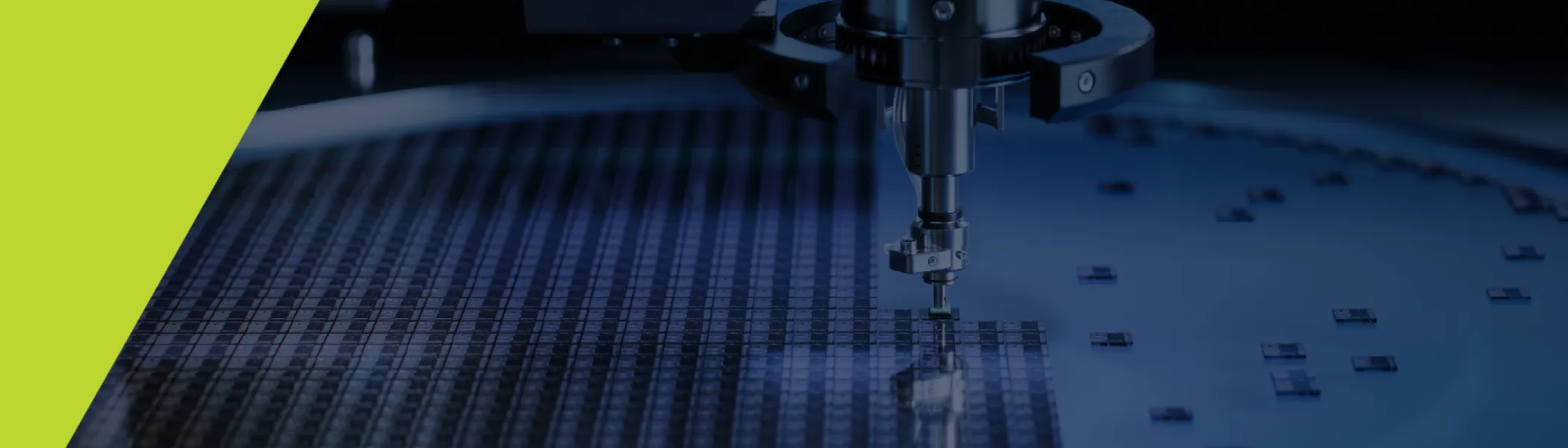
San Francisco, CA
United States
Course Description
This interactive course provides a practical, comprehensive overview of the semiconductor industry, with an emphasis on real-world applications, production processes, and the critical roles within semiconductor manufacturing. Attendees will gain insights into the global semiconductor value chain, from initial design and development to final product shipment, and explore how semiconductors power essential technologies in automotive, AI, and healthcare. The course covers emerging trends such as sustainable manufacturing, data-driven operations, and advanced node technology. Participants will also delve into key performance indicators (KPIs) for fab operations, R&D, and product development, and discover career paths and skill requirements within this dynamic industry.
Through engaging discussions, case studies, and hands-on exercises, participants will gain knowledge that can be immediately applied to their roles, empowering them to better understand semiconductor manufacturing’s impact and contribute to their organization’s success.
Learning Objectives
Identify key applications of semiconductors across industries
Map the semiconductor value chain from design to shipment
Gain understanding of smart manufacturing and resource-efficient production
Interpret KPIs for fab operations, product development, and R&D
Understand key roles and skills within the semiconductor industry
Who Should Attend
This course is ideal for industry newcomers, career changers, recent graduates, technical professionals from related fields, business leaders, and educators seeking a practical, comprehensive understanding of semiconductor applications, processes, roles, and industry dynamics.
- Industry Newcomers: Individuals new to the semiconductor field who need a comprehensive overview of applications, production processes, and key roles.
- Early- and Mid-Career Semiconductor Employees: Current employees seeking to deepen their understanding of the semiconductor value chain, industry challenges, and emerging trends.
- Career Changers and Recent Graduates: Those entering the semiconductor industry or recent graduates looking for insights into industry roles and required skills.
- Professionals from Related Fields: Technical professionals in areas like automotive, medical devices, consumer electronics, or engineering who want to understand semiconductor applications and manufacturing.
- Managers and Business Leaders: Leaders in strategy, business development, or operations who need to understand semiconductor production dynamics, KPIs, and sustainability to enhance profitability and competition.
- Educators and Trainers: Instructors teaching semiconductor technology who want a practical, industry-focused course structure.
Course Topics
- Introduction to Semiconductor Applications and Market Impact
- Semiconductor Value Chain: From Design to Shipment
- Smart Manufacturing and Technology Evolution
- Fab Operations and Facility Layout
- Key Performance Indicators for Semiconductor Functions
- Quality Assurance and Continuous Improvement
- Workforce Roles and Skills in Semiconductor Manufacturing
- Emerging Trends and Future Opportunities
- Closing and Immediate Application Planning
Instructor

Dr. Sirisha Kuchimanchi
Sahita Technologies
Important Information
Note that only the person who registered will receive a certificate of completion. This virtual training will not be recorded. Attendees must be present to access course knowledge.
Can't find the training link day of? After you register, you will receive the link to the live training via the email address you provided. In addition, you will receive email reminders about 24 hours in an advance and an hour before with the same link. Please keep these emails on hand to access the trainings on time. If you do not see any confirmation emails, please check your junk/spam folders before contacting SEMI U for support.
United States
SEMI UInterested in learning about the semiconductor ecosystem as a whole? This course introduces you to the basics of semiconductors, applications of semiconductors, front-end and back-end processing, fabrication facilities, process control and yield management, jobs and roles within the semiconductor industry, and what life is like working in a fab. Great for anyone seeking an understanding of an overview of the industry.
Pricing
- Members: $249
- Non-Members: $299
* For group orders with 10+ attendees, and for Students/Veterans discounted pricing, please contact [email protected]
8:00 am - 12:00 pm Off Add to Calendar 2026-11-04 08:00:00 2026-11-04 12:00:00 Semiconductor Ecosystem Overview (Americas & EU) 11/4 Interested in learning about the semiconductor ecosystem as a whole? This course introduces you to the basics of semiconductors, applications of semiconductors, front-end and back-end processing, fabrication facilities, process control and yield management, jobs and roles within the semiconductor industry, and what life is like working in a fab. Great for anyone seeking an understanding of an overview of the industry. PricingMembers: $249Non-Members: $299* For group orders with 10+ attendees, and for Students/Veterans discounted pricing, please contact [email protected] United States SEMI.org [email protected] America/Los_Angeles public America/Los_AngelesCourse Description
This course provides a comprehensive introduction to semiconductor manufacturing, guiding participants through the complete journey from silicon fundamentals to chip fabrication and packaging. Designed for professionals new to the semiconductor industry, the course explains key concepts, terminology, devices, and manufacturing processes used in modern fabs.
Who Should Attend
Anyone interested in understanding semiconductor manufacturing, including new employees, professionals in related industries, and those seeking to broaden their knowledge of the field.
Learning Objectives
Upon completion of the course, participants should be able to:
- Explain fundamental semiconductor concepts, including silicon materials, doping, PN junctions, and basic device behavior.
- Identify and correctly use common semiconductor manufacturing terminology.
- Outline the key steps involved in front-end wafer fabrication, from bare silicon to patterned wafers.
- Summarize back-end manufacturing processes, including assembly, packaging, and testing.
Topics Included
- Basic Electronics and Microelectronics
- Process Nodes
- Device Physics and Transistor Operation
- Crystal Growth and Wafer Preparation
- Advanced Transistor Technologies
- Circuit Design and Layout
- Wafer Processing
Important Information
Note that only the person who registered will receive a certificate of completion. This virtual training will not be recorded. Attendees must be present to access the course knowledge.
Can't find the training link on the day of the training? After you register, you will receive the link to the live training via the email address you provided. In addition, you will receive email reminders 24 hours in advance and 1 hour before, with the same link. Please keep these emails on hand to access the training on time. If you do not see any confirmation emails, please check your junk/spam folders before contacting SEMI U for support.

Singapore
- SEMI UStrengthen your knowledge and skills by learning about the journey from silicon fundamentals to chip fabrication and packaging.
Pricing
- Members: $399
- Non-Members: $449
* For group orders with 10+ attendees, and for Students/Veterans discounted pricing, please contact [email protected]
3:00 pm - 7:00 pm Off Add to Calendar 2026-10-27 15:00:00 2026-10-30 19:00:00 Inside the Fab: An Introduction to Semiconductor Manufacturing (Asia) 10/27 Strengthen your knowledge and skills by learning about the journey from silicon fundamentals to chip fabrication and packaging. Pricing Members: $399Non-Members: $449* For group orders with 10+ attendees, and for Students/Veterans discounted pricing, please contact [email protected] Singapore SEMI.org [email protected] Asia/Singapore public Asia/SingaporeCourse Description
This course will stress the impace of the IC and End product requirements, i.e., smaller, better, cheaper" and their influence on the manufacturing processes. Topics include area packaging - ball grid arrays, flip chip, fanout, attaching dies and chip scale packages, and the assembly technologies - chip & wire, tape automated bonding, and flip chip, as well as emerging technologies, namely, 3-D and stacked die, and packaging reliability issues.
Who Should Attend
This course is intended for both manufacturing and R&D know-how in IC packaging professionals, including but not limited to:
- Engeineers
- Managers
- Process Engineers
- R&D Engineers
- Sales and Application Engineers who supply packaging materials and tools
Learning Objectives
- Identify the wide variety of package types and how they align with different application uses.
- Understand chip interconnection technologies (such as wirebond, flip chip, or thin film) and chip encapsulation
- Identify the materials and processes used in packaging.
- Summarize the current state of the art packages, such as chiplets and heterogeneous packaging.
Gain a foundational understanding of what packaging is and its importance to the microelectronics industry.
Important Information
Note that only the person who registered will receive a certificate of completion. This virtual training will not be recorded. Attendees must be present to access the course knowledge.
Can't find the training link on the day of? After you register, you will receive the link to the live training via the email address you provided. In addition, you will receive email reminders about 24 hours in advance and an hour before with the same link. Please keep these emails on hand to access the training on time. If you do not see any confirmation emails, please check your junk/spam folders before contacting SEMI U for support.
Featured Speakers

Dr. Terry Alford
PT International LLC
Biography
United States
Strengthen your knowledge and skills by learning about IC packaging, assembly, and package/substrate and Heterogeneous Integration & Chiplets.
Pricing
Early Bird Pricing $100 off
- Members: $
845$745 - Non-Members: $
945$845
* For group orders with 10+ attendees, and for Students/Veterans discounted pricing, please contact [email protected]
7:30 am - 11:30 am Off Add to Calendar Disabled America/Los_Angeles Register NowCourse Description
This course offers a solid foundation in semiconductor manufacturing, from basic concepts to advanced techniques, providing practical insights into the tools, processes, and technologies driving the industry.
Learning Objectives
- Gain a comprehensive understanding of the semiconductor industry and manufacturing process, design, and eco-system of the semiconductor industry
- Understand the jargon, tools, and materials used in the design and fabrication of an integrated chip
- Effectively be able to communicate semiconductor manufacturing concepts with other associates and industry professionals
Course Topics
- Basic Electronics and Microelectronics: Definitions of essential electronic terms/concepts and introduction to microelectronics and integrated circuits
- Process Nodes: Process nodes and their impact on device performance and cost
- Device Physics and Transistor Operation: Principles of device operation and transistor functionality
- Crystal Growth and Wafer Preparation: Crystal growth techniques and wafer preparation processes
- Advanced Transistor Technologies: FDSOI, FinFETs, and Gate-All-Around (GAA) transistors and their impact on device performance
- Circuit Design and Layout: Introduction to circuit design, layout techniques, and tools
- Wafer Processing: Mask Making and Lithography: Techniques and materials used in mask making and various lithographic methods (DUV, Immersion, EUV)
- Clean Room Environments: Importance of clean rooms in semiconductor manufacturing and contamination issues
- Etching and Cleaning Processes: Plasma and wet etching processes
- Ion Implantation and Diffusion Techniques: Methods for doping and controlling diffusion in semiconductor fabrication
- Deposition Techniques: RTP, CVD, ALD, and ALE techniques and their effect on device performance
- Electroplating and Sputtering: Metal deposition techniques used in manufacturing
- Packaging and Testing: Techniques such as wire bonding, die stacking, flip chip, and chiplets packaging, semiconductor testing processes
- Metrology and Measurement Tools: Tools and methods used for precision measurement in semiconductor manufacturing
- Semiconductor Industry Ecosystem: The major players in the industry
Who Should Attend
Anyone interested in understanding semiconductor manufacturing, including new employees, professionals in related industries, and those seeking to broaden their knowledge of the field.
Instructor

Denny Frye
PT International, LLC
Testimonials
See what course participants had to say about this course!
- "The expansive width of coverage with sufficient depth; well curated, relevant information with live references, and the open style of delivery which made the course more of a sharing than a lecture, was enjoyable."
- "Denny's knowledge and ability to explain things in simplified ways was awesome!"
- "I really enjoyed going over the topics and watching the in-depth videos. I also liked how we received the slide information prior to the class."
- "The range of topics was perfect for an intro course."
- "Denny did a great job explaining complex topics. The opportunity to ask questions directly was beneficial for the entire class. If a question couldn't be answered immediately, it was addressed by the next break at the latest."
- "Thank you very much for the informative course. I appreciate the in-depth and in-detail insight in all aspects of Semiconductor Manufacturing!"
Important Information
Note that only the person who registered will receive a certificate of completion. This virtual training will not be recorded. Attendees must be present to access course knowledge.
Can't find the training link day of? After you register, you will receive the link to the live training via the email address you provided. In addition, you will receive email reminders about 24 hours in an advance and an hour before with the same link. Please keep these emails on hand to access the trainings on time. If you do not see any confirmation emails, please check your junk/spam folders before contacting SEMI U for support.
Germany
- SEMI UGain a comprehensive understanding of the semiconductor industry and the integrated circuit (IC) manufacturing process. This course is designed for new personnel in the field or anyone seeking a well-rounded knowledge of the tools, materials, and terminology used in semiconductor manufacturing.
Pricing
Early Bird Special - $100 off
- Members:
$995$895 - Non-Members:
$1095$995
* For group orders with 10+ attendees, and for Students/Veterans discounted pricing, please contact [email protected]
8:00 am - 5:00 pm Off Add to Calendar 2026-09-15 08:00:00 2026-09-16 17:00:00 Overview of Semiconductor Manufacturing (Europe) Gain a comprehensive understanding of the semiconductor industry and the integrated circuit (IC) manufacturing process. This course is designed for new personnel in the field or anyone seeking a well-rounded knowledge of the tools, materials, and terminology used in semiconductor manufacturing.PricingEarly Bird Special - $100 off Members: $995 $895Non-Members: $1095 $995* For group orders with 10+ attendees, and for Students/Veterans discounted pricing, please contact [email protected] Germany SEMI.org [email protected] Europe/Berlin public Europe/Berlin Register NowCourse Description
The first part of the course provides a brief overview of semiconductor design and fabrication steps, encompassing IC design techniques, all wafer processing steps, assembly, and packaging. It delves into semiconductor jargon in laypeople terms, and various substrate types such as Si, SiGe, FDSOI, GaAs, SiC, GaN. Additionally, it discusses different types of transistors like pMOS, nMOS, Bipolar, BiCMOS, CMOS, FinFets, and GAA and their evolution and what applications they are used in.
The second part of the course focuses on semiconductor business aspects such as silicon economics, wafer processing costs, semiconductor revenue forecasts, driving forces in the industry, top semiconductor IDMs, market competitors based on market share, OEMs, foundries, top tool vendors, and Fabless companies. Addresses the fastest-growing semiconductor markets based on geographic locations and applications, identifies semiconductor competitors/customers, and discusses major semiconductor markets like Automotive, PC, Mobile, Memory, Wireless, Cell phones, Consumer, Gaming, AI, IoT, Digital TV, Radio, Automotive, MEMS, and Emerging Technology & Impact on Industry.
Learning Objectives
- Understand the fundamental principles and theories semiconductor technology.
- Communicate with other associates and understand wafer processing steps.
- Understand semiconductor business aspects such as silicon economics, wafer processing costs, semiconductor revenue forecasts, driving forces in the industry, top semiconductor IDMs, market competitors based on market share, OEMs, foundries, top tool vendors, and Fabless companies.
- Review the semiconductor eco-system as it relates to design and fabrication of a semiconductor device.
- Gain knowledge of major semiconductor markets like Automotive, PC, Mobile, Memory, Wireless, Cell phones, Consumer, Gaming, AI, IoT, Automotive, MEMS, and Emerging Technology & Impact on Industry.
- Demonstrate effective communication skills through written reports, presentations, and discussions related to semiconductor subjects.
- Collaborate effectively with peers in group projects or discussions regarding semiconductor subjects.
- Analyze and evaluate research literature in semiconductor technology.
- Develop critical thinking and problem-solving skills applicable to semiconductor technology.
Who Should Attend
This course is suitable for anyone seeking a better understanding of the semiconductor industry, market leaders, terminology, business, and the semiconductor ecosystem.
Instructor

Denny Frye
PT International, LLC
Testimonials
See what course participants had to say about this course!
- "Denny Frye knows so much about the history of the semiconductor industry that he was able to tie together many different industries and technologies that I have heard about but never knew how they were connected."
- "Great overview of the semiconductor industry & market."
- "This was a very detailed course on many facets of the industry, would recommend!"
- "It was a great mix of technical and overview of the key players in the market!"
- "Good blend on technical and commercial topics."
- "Excellent introduction to the semiconductor world."
- "Great session on the understanding of the semiconductor industry in a nutshell."
Important Information
Note that only the person who registered will receive a certificate of completion. This virtual training will not be recorded. Attendees must be present to access course knowledge.
Can't find the training link day of? After you register, you will receive the link to the live training via the email address you provided. In addition, you will receive email reminders about 24 hours in an advance and an hour before with the same link. Please keep these emails on hand to access the trainings on time. If you do not see any confirmation emails, please check your junk/spam folders before contacting SEMI U for support.
Germany
SEMI UEmbark on a journey through semiconductor design, manufacturing, and business in this illuminating course. Explore IC design techniques, transistor evolution, and market dynamics. Delve into substrate types and industry economics, discovering the fastest-growing markets and key players shaping the semiconductor landscape.
Pricing
Early Bird Special - $100 off
- Members:
$845$745 - Non-Members:
$945$845
* For group orders with 10+ attendees, and for Students/Veterans discounted pricing, please contact [email protected]
8:00 am - 5:00 pm Off Add to Calendar 2026-09-14 08:00:00 2026-09-14 17:00:00 Understanding Semiconductor Technology and Business (Europe) Embark on a journey through semiconductor design, manufacturing, and business in this illuminating course. Explore IC design techniques, transistor evolution, and market dynamics. Delve into substrate types and industry economics, discovering the fastest-growing markets and key players shaping the semiconductor landscape.PricingEarly Bird Special - $100 off Members: $845 $745Non-Members: $945 $845* For group orders with 10+ attendees, and for Students/Veterans discounted pricing, please contact [email protected] Germany SEMI.org [email protected] Europe/Brussels public Europe/Brussels Register NowCourse Description
The instructor discusses the applied aspects of plasma-assisted etching from a general point of view. The emphasis is on mechanistic understanding. The etching of Si and its compounds is covered in detail. The chemistries used in the etching of other technology-related materials such as Al, organics, and III-V compounds are summarized. Other topics presented include selectivity, loading, ARDE and feature scale problems, damage, and issues associated with high-density plasma RIE. A section on plasma diagnostics and ion-beam based etching methods is briefly discussed.
Learning Objectives
- Understand the fundamentals of dry etching and the basic concepts of plasma etching
- Understand the physics of rf glow discharges (both high and low density)
- Understand the surface science aspects of RIE including the role of energetic ions
- Recognize the factors which influence etching anisotropy
- Define the steps of plasma-surface chemistry leading to etching
Topics Covered
- Fluorocarbon plasma etching of Si and its compounds
- Selectivity, loading effects, and aspect ratio dependent etching
- Uniformity of etching, damage, feature charging issues, and particles
- Etching of other materials (Al, organics, III-V compounds, etc)
- Plasma diagnostics such as optical emission spectroscopy with actinometry, mass spectrometry and laser-induced fluorescence
- Issues in high density plasma etching, wall effects, and ion beam-based methods
- Deep Reactive Ion Etching (DRIE)
- Applications and processing etching using ALE
- End point detection
Who Should Attend
This course is intended for scientists, technicians and others working with or interested in the dry etching of materials in reactive gas glow discharges, particularly those who do not have extensive experience in the field.
Instructor

Richard Beaudry
PT International, LLC
Testimonials
See what previous course participants had to say about this training!
- "Instructors' Process and Hardware knowledge were impressive."
- "I finally gained a clear understanding of the RIE process."
- "The instructor had a very good knowledge of the content."
- "I had a great time to learn fundamental concepts of plasma etching course from SEMI."
- "The aspect of the course that I found most beneficial was the Bosch processing parameter discussions on profile management. This subject was clearly the expertise of the presenter who skillfully addressed my questions regarding the subject."
Important Information
Note that only the person who registered will receive a certificate of completion. This virtual training will not be recorded. Attendees must be present to access course knowledge.
Can't find the training link day of? After you register, you will receive the link to the live training via the email address you provided. In addition, you will receive email reminders about 24 hours in an advance and an hour before with the same link. Please keep these emails on hand to access the trainings on time. If you do not see any confirmation emails, please check your junk/spam folders before contacting SEMI U for support.
United States
- SEMI UThis course discusses the fundamentals of plasma assisted phenomena and reactive ion etching (RIE) processes. The emphasis is on the physical and chemical processes that determine the consequences of a reactive gas plasma/surface interaction. The role of energetic ions as encountered in RIE systems is discussed in detail and the factors which influence anisotropy of etching are highlighted. Plasma-assisted etching equipment is described including capacitively coupled, inductively coupled and wave-generated plasmas sources.
Pricing
- Members: $745
- Non-Members: $845
* For group orders with 10+ attendees, and for Students/Veterans discounted pricing, please contact [email protected]
8:00 am - 12:00 pm Off Add to Calendar 2026-08-25 08:00:00 2026-08-26 12:00:00 Plasma Etching, ALE, & RIE (Americas & EU) This course discusses the fundamentals of plasma assisted phenomena and reactive ion etching (RIE) processes. The emphasis is on the physical and chemical processes that determine the consequences of a reactive gas plasma/surface interaction. The role of energetic ions as encountered in RIE systems is discussed in detail and the factors which influence anisotropy of etching are highlighted. Plasma-assisted etching equipment is described including capacitively coupled, inductively coupled and wave-generated plasmas sources. PricingMembers: $745Non-Members: $845* For group orders with 10+ attendees, and for Students/Veterans discounted pricing, please contact [email protected] United States SEMI.org [email protected] America/Los_Angeles public America/Los_Angeles Register NowCourse Description
This course offers a solid foundation in semiconductor manufacturing, from basic concepts to advanced techniques, providing practical insights into the tools, processes, and technologies driving the industry.
Learning Objectives
- Gain a comprehensive understanding of the semiconductor industry and manufacturing process, design, and ecosystem of the semiconductor industry
- Understand the jargon, tools, and materials used in the design and fabrication of an integrated chip
- Effectively be able to communicate semiconductor manufacturing concepts with other associates and industry professionals
Course Topics
- Basic Electronics and Microelectronics: Definitions of essential electronic terms/concepts and introduction to microelectronics and integrated circuits
- Process Nodes: Process nodes and their impact on device performance and cost
- Device Physics and Transistor Operation: Principles of device operation and transistor functionality
- Crystal Growth and Wafer Preparation: Crystal growth techniques and wafer preparation processes
- Advanced Transistor Technologies: FDSOI, FinFETs, and Gate-All-Around (GAA) transistors and their impact on device performance
- Circuit Design and Layout: Introduction to circuit design, layout techniques, and tools
- Wafer Processing:
- Mask Making and Lithography: Techniques and materials used in mask making and various lithographic methods (DUV, Immersion, EUV)
- Clean Room Environments: Importance of clean rooms in semiconductor manufacturing and contamination issues
- Etching and Cleaning Processes: Plasma and wet etching processes
- Ion Implantation and Diffusion Techniques: Methods for doping and controlling diffusion in semiconductor fabrication
- Deposition Techniques: RTP, CVD, ALD, and ALE techniques and their effect on device performance
- Electroplating and Sputtering: Metal deposition techniques used in manufacturing
- Packaging and Testing: Techniques such as wire bonding, die stacking, flip chip, and chiplets packaging, semiconductor testing processes
- Metrology and Measurement Tools: Tools and methods used for precision measurement in semiconductor manufacturing
- Semiconductor Industry Ecosystem: The major players in the industry
Who Should Attend
Anyone interested in understanding semiconductor manufacturing, including new employees, professionals in related industries, and those seeking to broaden their knowledge of the field.
Instructor

Denny Frye
PT International, LLC
Important Information
Note that only the person who registered will receive a certificate of completion. This virtual training will not be recorded. Attendees must be present to access the course knowledge.
Can't find the training link day of? After you register, you will receive the link to the live training via the email address you provided. In addition, you will receive email reminders about 24 hours in an advance and an hour before with the same link. Please keep these emails on hand to access the training on time. If you do not see any confirmation emails, please check your junk/spam folders before contacting SEMI U for support.
United States
- SEMI UGain a comprehensive understanding of the semiconductor industry and the integrated circuit (IC) manufacturing process. This course is designed for new personnel in the field or anyone seeking a well-rounded knowledge of the tools, materials, and terminology used in semiconductor manufacturing.
Dates and Times
August 19, 2026 8:00 - 5:00PT
August 20, 2026 8:00 - 1:30 PT
Pricing
Early Bird Special! $100 off
- Members:
$995$895 - Non-Members:
$1,095$995
* For group orders with 10+ attendees, and for Students/Veterans discounted pricing, please contact [email protected]
Course Description
The first part of the course provides a brief overview of semiconductor design and fabrication steps, encompassing IC design techniques, all wafer processing steps, assembly, and packaging. It delves into semiconductor jargon in laypeople terms, and various substrate types such as Si, SiGe, FDSOI, GaAs, SiC, GaN. Additionally, it discusses different types of transistors like pMOS, nMOS, Bipolar, BiCMOS, CMOS, FinFets, and GAA and their evolution and what applications they are used in.
The second part of the course focuses on semiconductor business aspects such as silicon economics, wafer processing costs, semiconductor revenue forecasts, driving forces in the industry, top semiconductor IDMs, market competitors based on market share, OEMs, foundries, top tool vendors, and Fabless companies. Addresses the fastest-growing semiconductor markets based on geographic locations and applications, identifies semiconductor competitors/customers, and discusses major semiconductor markets like Automotive, PC, Mobile, Memory, Wireless, Cell phones, Consumer, Gaming, AI, IoT, Digital TV, Radio, Automotive, MEMS, and Emerging Technology & Impact on Industry.
Learning Objectives
- Understand the fundamental principles and theories semiconductor technology.
- Communicate with other associates and understand wafer processing steps.
- Understand semiconductor business aspects such as silicon economics, wafer processing costs, semiconductor revenue forecasts, driving forces in the industry, top semiconductor IDMs, market competitors based on market share, OEMs, foundries, top tool vendors, and Fabless companies.
- Review the semiconductor eco-system as it relates to design and fabrication of a semiconductor device.
- Gain knowledge of major semiconductor markets like Automotive, PC, Mobile, Memory, Wireless, Cell phones, Consumer, Gaming, AI, IoT, Automotive, MEMS, and Emerging Technology & Impact on Industry.
- Demonstrate effective communication skills through written reports, presentations, and discussions related to semiconductor subjects.
- Collaborate effectively with peers in group projects or discussions regarding semiconductor subjects.
- Analyze and evaluate research literature in semiconductor technology.
- Develop critical thinking and problem-solving skills applicable to semiconductor technology.
Who Should Attend
This course is suitable for anyone seeking a better understanding of the semiconductor industry, market leaders, terminology, business, and the semiconductor ecosystem.
Instructor

Denny Frye
PT International, LLC
Testimonials
See what course participants had to say about this course!
- "Denny Frye knows so much about the history of the semiconductor industry that he was able to tie together many different industries and technologies that I have heard about but never knew how they were connected."
- "Great overview of the semiconductor industry & market."
- "This was a very detailed course on many facets of the industry, would recommend!"
- "It was a great mix of technical and overview of the key players in the market!"
- "Good blend on technical and commercial topics."
- "Excellent introduction to the semiconductor world."
- "Great session on the understanding of the semiconductor industry in a nutshell."
Important Information
Note that only the person who registered will receive a certificate of completion. This virtual training will not be recorded. Attendees must be present to access course knowledge.
Can't find the training link day of? After you register, you will receive the link to the live training via the email address you provided. In addition, you will receive email reminders about 24 hours in an advance and an hour before with the same link. Please keep these emails on hand to access the trainings on time. If you do not see any confirmation emails, please check your junk/spam folders before contacting SEMI U for support.
United States
SEMI UEmbark on a journey through semiconductor design, manufacturing, and business in this illuminating course. Explore IC design techniques, transistor evolution, and market dynamics. Delve into substrate types and industry economics, discovering the fastest-growing markets and key players shaping the semiconductor landscape.
Pricing
Early Bird Pricing $100 off
- Members: $
845$745 - Non-Members: $
945$845
* For group orders with 10+ attendees, and for Students/Veterans discounted pricing, please contact [email protected]
8:00 am - 5:00 pm Off Add to Calendar 2026-08-18 08:00:00 2026-08-18 17:00:00 Understanding Semiconductor Technology and Business (Americas) Embark on a journey through semiconductor design, manufacturing, and business in this illuminating course. Explore IC design techniques, transistor evolution, and market dynamics. Delve into substrate types and industry economics, discovering the fastest-growing markets and key players shaping the semiconductor landscape.PricingEarly Bird Pricing $100 off Members: $845 $745Non-Members: $945 $845* For group orders with 10+ attendees, and for Students/Veterans discounted pricing, please contact [email protected] United States SEMI.org [email protected] America/Los_Angeles public America/Los_Angeles Register NowCourse Description
This workshop explores how advanced packaging is redefining the trajectory of Moore's Law. Participants will gain insight into cutting-edge approaches, such as heterogeneous integration and chiplet architectures, that enable continued performance growth beyond traditional scaling limits.
We will delve into key packaging, including wafer-level packaging, fan-out wafer and panel-level solutions, 3D integration, and embedded packaging- highlighting how each enhances transistor density and system performance, along with the associated technical challenges. The session will also cover next-generation interconnect and bonding techniques, including thermocompression and hybrid bonding used in advanced die-stacking solutions such as SoIC-X and SoIC-P.
In addition, the workshop will examine evolving interposer architectures (2.1D, 2.3D, 2.5D, and beyond), including platforms such as CoWoS-S, CoWoS-L, and CoWoS-R. It will also explore emerging interposer materials like glass substrates, covering their benefits, fabrication processes, technical challenges, and supply chain landscape in supporting the continued evolution of Moore's Law.
Who Should Attend
This course is intended for both manufacturing and R&D know-how in IC packaging professionals, including but not limited to:
- Directors
- Managers
- Process Engineers
- R&D Engineers
- Sales and Application Engineers who supply packaging materials and tools
Learning Objectives
- Understand the principles in the evolution of IC packaging and how the semiconductor industry has evolved with time.
- Understand the principles of Interconnections ranging from TAB, and Wirebond to various Flip Chip bonding, such as thermocompression bonding with NCP, C4, ACF for manufacturing and R&D development.
- Review the interposer of leadframe, ceramic, flex to BT substrates for Microelectronics packaging.
- Explain the assembly flow and new assembly techniques from backgrinding to singulation.
- Describe the material characterization from bulk to interfaces to reduce stress and enhance interfacial adhesion for reliability enhancement.
Course Topics
- Advanced packaging and material characterization.
- Packaging principles and how packaging evolves into heterogeneous packaging.
- Packaging concepts such as Fan-in, Fan-out WLP, Embedded packaging technology, 3D packaging, TSV.
- Wirebond and Flip chip interconnect technologies inclusive of interposer technologies, such as leadframe, ceramic, flex and substrate.
- Assembly processes from backgrinding to singulation for QFP and FBGA packages.
- Material characterization to select materials to reduce stress and strengthen the interface for reliability enhancement.
Instructor

Dr. Lee Teck Kheng
Institue of Technical Education
Important Information
Note that only the person who registered will receive a certificate of completion. This virtual training will not be recorded. Attendees must be present to access course knowledge.
Can't find the training link day of? After you register, you will receive the link to the live training via the email address you provided. In addition, you will receive email reminders about 24 hours in an advance and an hour before with the same link. Please keep these emails on hand to access the trainings on time. If you do not see any confirmation emails, please check your junk/spam folders before contacting SEMI U for support.
Singapore
SEMI UAs transistor scaling slows under the physical limits of lithography, the semiconductor industry is entering a new era-one where innovation is driven not just by node shrink, but by how chips are integrated and packaged.
Pricing
- Members: $599
- Non-Members: $649
* For group orders with 10+ attendees, and for Students/Veterans discounted pricing, please contact [email protected].
8:30 am - 5:00 pm Off Add to Calendar 2026-08-03 08:30:00 2026-08-03 17:00:00 Reshaping Moore's Law with Advanced Packaging (Asia) As transistor scaling slows under the physical limits of lithography, the semiconductor industry is entering a new era-one where innovation is driven not just by node shrink, but by how chips are integrated and packaged.PricingMembers: $599Non-Members: $649* For group orders with 10+ attendees, and for Students/Veterans discounted pricing, please contact [email protected]. Singapore SEMI.org [email protected] Asia/Singapore public Asia/Singapore Register Now