SEMICON Japan 2024 Opens Tomorrow to Highlight Smart Applications Powered by Semiconductor Technology
TOKYO – December 10, 2024 – SEMICON Japan, the region’s premier microelectronics industry conference and exhibition, opens tomorrow at Tokyo Big Sight. With more than 1,000 exhibitors from 35 regions, the conference gathers leaders from across the microelectronics manufacturing supply chain from December 11-13. SEMICON Japan 2024 will spotlight smart semiconductor applications for automotive, Internet of Things (IoT), and more, emphasizing industry insights, trends, and innovations that are powering the next wave of digital transformation. Registration is open.
Themed Strong Together, this year’s SEMICON Japan will feature two new events, including the Advanced Design Innovation Summit (ADIS) that will detail the future of semiconductor design and verification. Additionally, the inaugural SEMI Global Standards Summit will look at future advancements of semiconductor manufacturing and industry standardization strategies focusing on three important themes: Smart Manufacturing for Future Factories, Packaging Architectures & Materials, and Environmental Sustainability.
“Japan’s focus on worldwide semiconductor industry collaboration and its critical role in the broader supply chain solidify it as a key region for innovation,” said Jim Hamajima, President of SEMI Japan. “SEMICON Japan will expand opportunities to connect with leaders across the global industry to further accelerate the pace of technological developments in growing sectors such as AI, automotive, IoT, 5G, and more. As the world becomes increasingly digital, SEMICON Japan is bringing the industry together to drive the next wave of groundbreaking technology.”
Notable speakers at the SuperTHEATER, SEMICON Japan’s biggest stage, will include:
Akira Amari: Former Member of the House of Representatives Honorary Chairman, Diet Members Caucus for the Promotion of Semiconductor Strategy
Tetsuro Higashi: Chairperson of the Board, Rapidus Chairman, Leading-Edge Semiconductor Technology Center
Dario Gil: Senior Vice President and Director of IBM Research, IBM
Ho-Young Son: Vice President of Advanced Package Development, SK hynix
Terushi Shimizu: Representative Director, President and CEO, Sony Semiconductor Solutions
Concurrent Events with SEMICON Japan
Advanced Packaging and Chiplet Summit (APCS): This summit will include an exhibition area for technologies that support 2.5D, 3D, redistribution layers, through silicon vias, chiplets, and more. APCS will also feature networking opportunities and conference sessions led by the world’s top industry players.
FLEX Japan: This event will bring device and material suppliers together with vendors who provide the final products, with the goal of creating new business opportunities within the flexible device and printed electronics sectors.
Other SEMICON Japan Highlights
Workforce Development Programs*:SEMICON Japan’s workforce development programs will include Mirai College at SEMICON*, where 51 semiconductor-related companies will gather to help attendees learn about the industry. In addition, 70 universities* from across Japan will share their latest research and provide collaboration opportunities for those in academia*.
Technology Pavilions:The many technology pavilions at SEMICON Japan include the Quantum Computing, Ministry of the Environment, Power Electronics, Clean Room, and SEMI Sustainability HUB pavilions. Each pavilion will feature targeted exhibitions related to their focus area.
Interactive Attractions:To help encourage semiconductor industry interest among the younger generation, SEMICON Japan will feature Yoichi Ochiai’s Passion Lab, an initeractive discussion led by media artist, Yoichi Ochiai. In addition, SEMICON STADIUM will allow attendees to see, touch, and experience semiconductors through sports-playing AI robots, such as AI basketball robot “CUE6” (Toyota Motor Corporation), table tennis robot “Forpheus” (Omron), baseball swing analysis using Fujitsu Human Motion Analytics (Fujitsu), and the fastest robot to solve a puzzle cube “TOKUFASTbot” (Mitsubishi Electric).
SEMI® is the global industry association connecting over 3,000 member companies and 1.5 million professionals worldwide across the semiconductor and electronics design and manufacturing supply chain. We accelerate member collaboration on solutions to top industry challenges through Advocacy, Workforce Development, Sustainability, Supply Chain Management and other programs. Our SEMICON® expositions and events, technology communities, standards and market intelligence help advance our members’ business growth and innovations in design, devices, equipment, materials, services and software, enabling smarter, faster, more secure electronics. Visit www.semi.org, contact a regional office, and connect with SEMI on LinkedIn and X to learn more.
Contact Information:
Association Contacts
Shuichi Sato/SEMI Japan Phone: 81.3.3222.5757 Email: [email protected]
Siemens extends Veloce hardware-assisted verification and validation with new Innexis shift-left software
Innexis delivers a set of products and capabilities to address demand for shift-left software development in the IC development process
With more demanding software workloads, it is critical to facilitate the development and execution of realistic workloads early in the design phase to shorten overall development time and identify hardware and software defects earlier
Siemens Digital Industries Software announced today the Innexis product suite, a complement to its industry leading Veloce™ hardware-assisted verification and validation system.
Building on the success and rapid adoption of Veloce, Siemens’ Innexis product suite delivers a set of capabilities to address customer demand for shift-left software in the early phases of IC development. These products include a hardware/software development flow from virtual to hybrid to full RTL, an architecture native virtual platform for early high-speed software development and a simulation backplane that enables the development of digital twins in Siemens’ PAVE360™ software for software-defined vehicles and other complex systems.
“The complexity of integrated circuits (IC) is increasing exponentially, designers need more efficient methodologies to meet industry demands. Veloce has seen rapid adoption by industry leaders to help solve this critical bottleneck. The Innexis product suite extends workflow improvements from Veloce to help our customers shift left their IC development and debug cycle,” said Jean-Marie Brunet, vice president and general manager, Hardware-Assisted Verification, Siemens Digital Industries Software. “This enables IC design to begin months before final RTL, all while using a common software workload across the development process.”
Adoption of a shift-left approach for software development and IP verification processes is now mandatory. As chip designs become increasingly complex due to more demanding software workloads, it is critical to enable the development and execution of realistic workloads early in the design phase. A proactive shift-left software approach helps mitigate the risk of identifying issues late in the development cycle.
“The implementation of Innexis in our development process has significantly enhanced software and system validation performance, thereby improving the efficiency of our teams and projects. By enabling heterogeneous component modeling within virtual platforms, it allows us to create realistic high-speed models of System on Chips (SoCs),” said Ari Hautala, Principal System Architect, Nokia Mobile Networks. “Furthermore, the integration of these high-speed virtual platforms with RTL IP on Veloce emulators facilitates superior overall performance while still permitting precise cycle-accurate performance and power analysis on RTL model components. Additionally, Innexis offers exceptional visibility and debuggability for the SoC design, along with the capability to integrate and execute a large number of complex test cases effectively.”
Currently, the Innexis product suite consists of:
Innexis Developer Pro: Innexis Developer Pro software provides a connected development flow from virtual to hybrid to full RTL. This provides a comprehensive environment for accelerating the creation of complex SoC design supporting a wide range of use-cases including seamless hardware-software co-development, co-validation, and pre-silicon cycle accurate analysis and validation. Innexis Developer Pro supports the modelling of complex SoC’s with heterogeneous cores and custom SystemC model components. In addition, it provides the ability to run in both virtual plus RTL hybrid mode for high performance execution, and then at a time of interest switch to full RTL emulation enabling high accuracy analysis of the full SoC when required.
Innexis Architecture Native Acceleration (ANA): Innexis Architecture Native Acceleration software is a cloud- based high-speed virtual platform. By running natively on Arm based servers the software workloads run at much higher speeds than on typical instruction set simulation based virtual platforms. Cloud hosting also provides scalable compute resources and simple browser-based access and tools. Innexis Architecture Native Acceleration can also run on local Arm based servers if preferred. In both cases it enables early software development and testing, and early software defect identification.
Innexis Virtual System Interconnect: Innexis Virtual System Interconnect software facilitates the creation and simulation of comprehensive system level digital twin platforms by seamlessly connecting multi-behavioral virtual and physical subsystems, supporting a variety of communication protocols. Innexis Virtual System Interconnect behavioral models can include Innexis Developer Pro or Innexis Architecture Native Acceleration SoC models, supporting system-level shift-left software development and RTL verification.
To learn more about Siemens’ Innexis product suite and how it addresses the demand for shift-left software development in the integrated circuit development process, visit: www.siemens.com/innexis
About Siemens
Siemens Digital Industries Software helps organizations of all sizes digitally transform using software, hardware and services from the Siemens Xcelerator business platform. Siemens' software and the comprehensive digital twin enable companies to optimize their design, engineering and manufacturing processes to turn today's ideas into the sustainable products of the future. From chips to entire systems, from product to process, across all industries. Siemens Digital Industries Software – Accelerating transformation.
Note: A list of relevant Siemens trademarks can be found here. Other trademarks belong to their respective owners.
Heidelberg Instruments Reports Major Orders for the VPG+ 1400 FPD Volume Pattern Generator from Leading Asian Photomask Manufacturers
Heidelberg Instruments Reports Major Orders for the VPG+ 1400 FPD Volume Pattern Generator from Leading Asian Photomask Manufacturers
Heidelberg, Germany – Heidelberg Instruments has secured two major orders for its VPG+ 1400 FPD Volume Pattern Generator from leading photomask manufacturers in Asia, with a total order value between EUR 9 million and EUR 10 million. Deliveries are scheduled for 2025.
“These significant order intakes mark major milestones for the company, reinforcing our market position and driving further innovation and growth in the display technology sector”, says Alexander Forozan, VP of Global Sales and Business Development.
The VPG+ 1400 is Heidelberg Instruments’ largest system, specifically designed for large-format photomask patterning in the flat panel display (FPD) industry. It supports mask sizes up to 1400 x 1400 mm², making it ideal for various flat panel display generations (G4 to G8). The VPG+ 1400 sets a new standard for high-throughput photomask production, offering the precision and scalability required for large displays. Additionally, it delivers the accuracy needed to produce large-area halftone photomasks for flat panel displays.
Equipped with advanced metrology and alignment features, including Cognex AI-based image recognition, the system ensures precise alignment for multilayered masks. Its linear and nonlinear coordinate corrections further enable precise overlay across tools.
By addressing the diverse exposure needs of customers, Heidelberg Instruments' large-area VPG+ Volume Pattern Generators have proven to be valuable assets in display photomask production lines.
From Concept to Reality: Advancing Digital Twin in Semiconductor Manufacturing
This event is now sold out. Please register if you'd like to receive access to presentation materials.
SEMI Member: $225
Non-Members: $295
Cancellations received on or before November 17, 2023 will be fully refunded. After this date, only substitutions will be accepted.
Please email your cancellation request to Agnes Cobar at [email protected]. Refunds will not be issued for cancellations (including no-shows) made after November 17th, 2023.
Substitutes are only accepted with written permission from the original registrant.
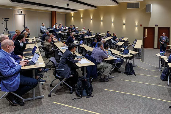
Digital Twin technology has gained significant traction in a variety of industries and is now in its early stages of adoption by the semiconductor industry. In this workshop, we will hear from across the ecosystem (OEMs, Platforms, end users, and more) as to the various levels of Digital Twins needed, the development challenges, opportunities, and recommendations. The development of full tool or full-process level semiconductor digital twins is challenging but has the potential to significantly improve the productivity & quality of operations.
Primarily beneficial for developers, and end-users of DT’s to attend so that we can understand the challenges, and scope of development effort required to create and deploy such DT systems in manufacturing.
Hosted by the SEMI Smart Manufacturing Initiative.
SEMI HQ 673 S Milpitas Blvd. Milpitas, CA95035 United States
Morning, Day 1: December 4, 2024
8:00 am
-
12:20 pm
Equipment Level Digital Twins (Equipment Makers)
Digital twins from equipment makers are virtual replicas of their physical products. They are created using data collected from sensors on the equipment, as well as from design and engineering drawings.
8:00 am
-
9:00 am
Registration & Breakfast
9:00 am
-
9:15 am
Mark Da Silva
SEMI
Welcome All
9:15 am
-
9:40 am
Supika Mashiro
Sr. Expert/TEL, Co-chair of the IRDS Factory Integration IFT (Focus Team)
TEL
Emergence of Digital Twin technology in the IRDS Factory Integration focus roadmap
9:40 am
-
10:05 am
Ala Moradien
Director, CAE Programs and Digital Twin Initiatives
Applied Materials
AppliedTwin™: A Digital Twin Platform for Semiconductor Manufacturing, Use Case in Sustainability
10:05 am
-
10:30 am
Joe Ervin
Senior Director and Product Line Head, Semiverse™ Solutions
Lam Research
A Single Digital Twin for Semiconductor Manufacturing? Semiverse™ Solutions and Building the Digital Family
10:30 am
-
10:45 am
Coffee Break
10:45 am
-
11:10 am
Sean Glazier
Software Engineer IV
Onto Innovation
Building a digital twin model is EASY. Getting the model deployed and used every day, now that’s the challenge
11:10 am
-
11:35 am
Basil Milton
Senior Manager, Ball Bonder Process R&D
Kulicke & Soffa
Digital Twin Improvements for Wire Bond Process Optimization
11:35 am
-
12:20 pm
Moderator
Mark Huntington
McKinsey
Open Forum/Panel/Breakout
12:20 pm
-
1:30 pm
Lunch
Afternoon, Day 1: December 4, 2024
1:30 pm
-
5:00 pm
Chamber Process, Operations & Planning Level Digital Twin (Solution Providers)
Solution providers offer a variety of products and services to help companies implement and manage digital twins (physics-based process models for components or sub-systems).
1:30 pm
-
1:55 pm
Sarbajit Ghosal
Lead Research Engineer
SC Solutions, Inc.
Fast, Physics-based Models for Real-time Process Control And Monitoring
1:55 pm
-
2:20 pm
Norman Chang
Ansys/IEEE Fellow and Chief Technologist of Electronics, Semiconductor, and Optics BU
Ansys Inc.
Enabling ML-augmented Digital Twin for Semiconductor Manufacturing
2:20 pm
-
2:45 pm
Holland Smith
Director of Technical Marketing, INFICON IMS (Intelligent Manufacturing Systems)
INFICON
The Operations Digital Twin: Why Every Factory Needs One, and Why Many Don't Have One (Yet)
2:45 pm
-
3:00 pm
Coffee Break
3:00 pm
-
3:25 pm
Chandra Reddy
Senior Technical Staff Member, AI Applications
IBM Research
Generative AI enabled Digital Twins
3:25 pm
-
3:50 pm
Jon Herlocker
Founder & CEO
Tignis
Practical Machine Learning Applications for the Process Modelling and Optimization of Manufacturing Process Tools and Process Lines
3:50 pm
-
4:15 pm
Ken Smerz
CEO
Zelus
Digital Twin Creation and Application
4:15 pm
-
5:00 pm
Moderator
John Behnke
GM FPS Product Line
INFICON
Open Forum/Panel/Breakout
5:00 pm
-
7:00 pm
Networking Reception
Morning, Day 2: December 5, 2024
8:00 am
-
12:20 pm
DT Adoption & Implementation (Device Makers)
As a device maker, a digital twin is a critical tool for improving productivity, quality, and efficiency. A digital twin is a virtual representation of your physical devices or fab, and it can be used to simulate and optimize operations.
8:00 am
-
9:00 am
Breakfast
9:00 am
-
9:05 am
Mark Da Silva
SEMI
Day 2 - Welcome
9:05 am
-
9:30 am
Prof. Phillip Wong
Professor of Electrical Engineering, Willard R. and Inez Kerr Bell Professor in the School of Engineering Stanford University
Stanford
A Vision for the Future Semiconductor Fab
9:30 am
-
9:55 am
Steven J Meyer
General Manager and Sr. Principal Engineer, Advanced Industrial Systems
Intel Corporation
High Value from Digital Twins in Semiconductor Manufacturing
9:55 am
-
10:20 am
Jae Y. Park
VP of Technology
Samsung
AI Powered Digital Twin: Transforming Smart Manufacturing
10:20 am
-
10:45 am
Coffee Break
10:45 am
-
11:10 am
Rosa Javadi
Principal Engineer
Jabil
Smart Manufacturing Technology for Complex Integrated Systems
11:10 am
-
11:35 am
Amit Lal
Professor
Cornell University
Peter Doerschuk
Professor
Cornell University
Ben Davaji
Assistant Professor
Northeastern University
Digital Twin Frameworks for an Academic Research and Development Cleanroom
11:35 am
-
12:20 pm
Moderator
Bobby Mitra
Deloitte
Open Forum/Panel Discussion - Developing Full Process Level Digital Twin – Challenges
12:20 pm
-
1:30 pm
Lunch
Afternoon, Day 2: December 5, 2024
1:30 pm
-
5:00 pm
DT Connectivity and Platform Integration (Cloud, Facilities, & Supply Chain)
Solution providers offer a variety of products and services to help companies implement and manage digital twins including integration, connectivity, & security including horizontal integration across the supply chain.
1:30 pm
-
1:55 pm
Rad Desiraju
Director , WW Industry Advisory
Microsoft
Unlocking Innovation with Digital Twins
1:55 pm
-
2:20 pm
Gautham Unni
Head of Solutions & Business Development (Semiconductor)
AWS
Accelerate your Digital Twin journey with AWS
2:20 pm
-
2:45 pm
David Gross
Portfolio Development Executive, Manufacturing Digitalization, Semiconductor Industry
Siemens
Srividya Jayaram
Principal Product Engineering ManagerSiemens EDA
Siemens EDA
Siemens: Accelerating technology From Design to HVM
2:45 pm
-
3:00 pm
Coffee Break
3:00 pm
-
3:25 pm
Slava Libman
CEO
FTD Solutions INC
Digital Twins Enabling Environmental Sustainability
3:25 pm
-
3:50 pm
Becky Kelderman
Manager
Rockwell Automation
The Nimble Supply Chain with Digital Twin
3:50 pm
-
4:15 pm
Ram Walvekar
VP and PLM Head, Digital Transformation Unit
HCL Technologies
Integrated Cognitive Digital Twin for Semiconductor Equipment
4:15 pm
-
5:00 pm
Paul Trio - Moderator
SEMI
Required Standards for Digital Twin Technology - Open Forum/Panel/Breakout
-
Join us for a 2-day deep dive into the expanding world of Digital Twin (DT) technology in the semiconductor realm. Understand its potential challenges and opportunities, and discover its transformative power in enhancing operational productivity and quality. Calling all DT developers and end-users: collaborate, learn, and pave the way for DT's integration into manufacturing!
This event is now sold out. Please register if you'd like to receive notifications about available spaces or access to presentation materials.
From Concept to Reality: Advancing Digital Twin in Semiconductor Manufacturing
[IN-PERSON EVENT]
December 4-5, 2024
8:00 AM – 5:00 PM PT
8:00 am - 5:00 pm
Off
Add to Calendar2024-12-04 08:00:002024-12-05 17:00:00From Concept to Reality: Advancing Digital Twin in Semiconductor ManufacturingJoin us for a 2-day deep dive into the expanding world of Digital Twin (DT) technology in the semiconductor realm. Understand its potential challenges and opportunities, and discover its transformative power in enhancing operational productivity and quality. Calling all DT developers and end-users: collaborate, learn, and pave the way for DT's integration into manufacturing!
This event is now sold out. Please register if you'd like to receive notifications about available spaces or access to presentation materials.SEMI HQ 673 S Milpitas Blvd. Milpitas, CA 95035 United StatesSEMI.org[email protected]America/Los_Angelespublic
America/Los_Angeles
On-demand
2025 Technology Workshops Shaping the Future of Electronics
Registration
Early Bird Pricing (until March 25, 2025) $375 members $525 non-members
Regular Pricing (After March 25, 2025) $525 members $699 non-members
MDM2 members please contact Michelle Fabiano, [email protected], for discount information.
Complimentary student registration is available but has limited capacity. Students can Register here to be contacted about complimentary attendance after March 15th.
Cancellation Policy
Cancellations received on or before March 25, 2025, are fully refunded with a $50 processing fee. Refunds will not be issued for cancellations (including no-shows) made after March 25, 2025, and only substitutions are accepted with a written note from the registered attendee. Please email your cancellations or substitutions on company letterhead to Michelle Fabiano at [email protected].
Industry Tours Take advantage of an exclusive industry tour at Medtronic on April 21, just before our workshop begins! Please note that space is limited and transportation will not be provided. Don't miss this unique opportunity!
Shaping the Future of Flexible Hybrid Electronics: FHE Technical Gap Analysis workshop Join us on April 22 for a focused technical gap analysis workshop on Flexible Hybrid Electronics (FHE) to shape FlexTech’s 2025 Request for Proposals (RFP). With a history of over five dozen R&D projects, FlexTech has driven advancements in flexible batteries, energy harvesting, and system integration. Hear from principal investigators on the latest developments and join breakout sessions to explore challenges, gaps, and priorities for future innovation with industry, government, and academic leaders.
Why Attend: Contribute to FlexTech’s 2025 priorities, learn about cutting-edge developments, and Join breakout sessions and network with key experts.
The day will conclude with a Mayo Clinic Lab for function tour followed by a Student Poster Networking Reception.
Advancing Human Performance Technologies: NBMC Technical Gap Analysis Workshop Join us on April 23 for the Nano-Bio Materials Consortium (NBMC) Technical Gap Analysis Workshop, a focused forum on wearables and bio-signal sensing technologies for real-time cognitive and physical state monitoring, augmentation, and intervention. Participants will address critical technical gaps in preparation for the next NBMC Request for Proposal.
NBMC brings together industry, government, and academia to advance early-stage nano and bio technologies, driving innovations in low-cost wearable sensors and communication systems through over three dozen R&D projects.
The day will conclude at the Phoenix Bioscience Core, located in the heart of the innovator's district in downtown Phoenix, Attendees will enjoy guided tours, a reception and a keynote presentation on "Bridging Clinical Needs and Emerging Technology: Emerging Device-Based Health Intervention Platforms: Wearables, Robotics, and BioHybrids." Networking opportunities will be available throughout these activities.
Clinician Insights Shaping the Future of Electronics: MDM2 and Smart MedTech Forum Join us on April 24, for an inspiring and dynamic session spotlighting the collaboration between MDM2 (Medical Device Manufacturing Multiplier ) and the Smart MedTech Initiative. This forum highlights the critical role of clinician and patient perspectives in driving innovation for next-generation medical devices.
Together, MDM2—a consortium dedicated to positioning Greater Phoenix as a leading hub for digital medical device manufacturing—and SEMI Smart MedTech Initiative are working to bridge the gap between emerging technologies and real-world needs. Discussions will explore how clinician insights can spark innovation in medical devices, accelerate technology adoption and commercialization and leverage AI and machine learning to advance manufacturing processes.
An evening event will be hosted by Venture Cafe at the end of the workshop to engage with the local innovation community.
Including with registration are breakfasts, breaks, lunches and receptions.
ASU Health Futures Center 6161 E Mayo Blvd Phoenix, AZ85054 United States
Monday, April 21 (Medtronic Tour)
2:00 pm
Medtronic Tour
(Tour sold out. Sign up for the waitlist.)
Join us for an exclusive one-hour tour of Medtronic’s facility, to explore its advanced operations in designing and manufacturing microelectronics for implantable medical devices.
Attendees will break into groups for smaller discussions to identify challenges, prioritize those challenges and identify opportunities on critical issues discussed throughout the morning session.
3:05 pm
-
3:20 pm
Break
3:20 pm
-
4:10 pm
Breakout Sessions Readout
4:30 pm
-
6:00 pm
Student Poster Networking Reception & Mayo Clinic Lab for Function Tour
Mayo Clinic
IERB Building
5951 E. Mayo Blvd
Phoenix, AZ 85054
Mayo Lab Tour: If you're interested, please sign up at the registration desk. Space is limited to 20 participants and will be available on a first-come, first-served basis.
Note: Transportation to this reception will not be provided. (2 minute drive.)
Attendees will break into groups for smaller discussions to identify challenges, prioritize those challenges and identify opportunities on critical issues discussed throughout the morning session.
3:05 pm
-
3:20 pm
Break
3:20 pm
-
4:10 pm
Breakout Sessions Readout
5:00 pm
-
7:00 pm
Networking Reception and Tours of Wexford Connect
Enjoy Networking, concurrent tours, and presentation content
850 Phoenix Bioscience Core
850 N 5th Street
Phoenix, AZ 85004 https://850pbc.com
5:00 pm - 5:30 pm: Tours of Wexford Connect (Limited to 30 people)
6:15 pm - 7:00 pm: Panel Discussion:
Bridging Clinical Needs and Emerging Technology: Research, Implementation, and Scale. Moderator: Chris Yoo, General Partner, Xcellerant Ventures Panelists: Suman Bose, Assistant Professor of Biomedical Engineering, Mayo Clinic Hakan Ceylan, Assistant Professor and Principal Investigator, Mayo Clinic Ross Bundy, CEO, CRISPRQC Elsa Abruzzo, CEO, Anuncia Medical Allen Waziri, CEO and Co-Founder, iCE Neurosystems
Note: Transportation will not be provided. (30+ minute drive.)
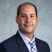
Panel Discussion: The Arizona MDM2 Consortium - Investing in the Medical Technology Manufacturing Renaissance
Moderator: Chris Yoo, Founder and CEO and Regional Innovation Officer, MDM2 Consortium Panelists: Kiran Avancha, Chief Innovation Officer, HonorHealth Rochelle Rivas, District Director for Healthcare Innovation, Maricopa Community Colleges Alex Tessmer, Associate Director, BD Peripheral Intervention, Ideation
9:45 am
-
10:10 am
Jonathon Parker
Neurosurgeon, Director of Device-Based Neuroelectronics Lab
Mayo Clinic, Arizona
Aman Verma
Hospitalist
Mayo Clinic, Arizona
FIRESIDE CHAT: How can wearables and implantables improve care of the acutely ill patient?
Moderator: Jonathon Parker , Neurosurgeon, Director of Device-Based Neuroelectronics Lab, Mayo Clinic - Arizona Participants: Aman Verma, Hospitalist, Mayo Clinic, Arizona
10:10 am
-
10:25 am
Break
10:25 am
-
11:10 am
Moderator
Kiran Avancha
Chief Innovation Officer
Honor Health Innovations
Craig Norquist
Chief Innovation Officer
Honor Health
Matthew Anderson
Chief Medical Information Officer - Ambulatory
Honor Health
PANEL DISCUSSION: Health Data 2035: How do we Capture, Integrate, and Secure Health Data Streams From Wearables and Implantables to Improve Patient Care?
Moderator: Kiran Avancha, Chief Innovation Officer, Honor Health Innovations Panelists: Craig Norquist, Chief Innovation Officer, Honor Health Matthew Anderson, Chief Medical Information Officer - Ambulatory, Honor Health
11:10 am
-
11:45 am
Jonathon Parker
Neurosurgeon, Director of Device-Based Neuroelectronics Lab
Mayo Clinic, Arizona
Bart M. Demaerschalk
Vascular Neurologist
Mayo Clinic, Arizona
Chandan Krishna
Neuro-endovascular Neurosurgeon
Mayo Clinic - Arizona
FIRESIDE CHAT: Stroke Care 2035- How Can Digital Health Data Transform Stroke Care?
Moderator: Jonathon Parker , Neurosurgeon, Director of Device-Based Neuroelectronics Lab, Mayo Clinic - Arizona Participants: Bart M. Demaerschalk, Vascular Neurologist, Mayo Clinic, Arizona Chandan Krishna, Neuro-endovascular Neurosurgeon, Mayo Clinic, Arizona
11:45 am
-
12:15 pm
Jonathon Parker
Neurosurgeon, Director of Device-Based Neuroelectronics Lab
Mayo Clinic, Arizona
Nandita Khera
Oncologist, Associate Chair of Digital Health
Mayo Clinic
FIRESIDE CHAT: Real-Time Oncology - How Can Wearables and Implantables Reshape Oncology Care in 2035?
Moderator: Jonathon Parker , Neurosurgeon, Director of Device-Based Neuroelectronics Lab, Mayo Clinic - Arizona Participants: Nandita Khera, Oncologist, Associate Chair of Digital Health, Mayo Clinic
12:15 pm
-
1:00 pm
Moderator
Randal Schulhauser
Founder and CEO
Schulhauser Associates LLC
Jonathon Parker
Neurosurgeon, Director of Device-Based Neuroelectronics Lab
Mayo Clinic
Allen Waziri
Neurosurgeon, Co-Founder iCE Neurosystems
iCE Neurosystems
Paul Gerrish
VP, Technology and Medtronic Fellow
Medtronic
Panel Discussion: The New Frontier of Long-Term Brain Monitoring: Brain Computer Interface Re-Imagined
Moderator: Randal Schulhauser, Founder and CEO, Schulhauser Associates LLC Panelists: Jonathon Parker, Neurosurgeon, Director of Device-Based Neuroelectronics Lab, Mayo Clinic Allen Waziri, Neurosurgeon, Co-Founder iCE Neurosystems, iCE Neurosystems Paul Gerrish, VP, Technology and Medtronic Fellow, Medtronic
Division Director, Integrative Health and Performance Sciences
BlueHalo
Deon Chen
Sr. Manager, HEOR Strategic Planning
BD
Panel Discussion: Digital Health Revolution: Insights and Innovations
Moderator: Douglas Kiehl, BioCrossroads/Purdue Panelists: Bharath Rajagopalan , Director – Strategic Marketing, Health & Wellness, STMicroelectronics Anirban Bandyopadhyay, Senior Director, Global Foundries Stephaney Shanks, Division Director, Integrative Health and Performance Sciences, BlueHalo Deon Chen, Sr. Manager, HEOR Strategic Planning, BD
4:30 pm
-
7:00 pm
Evening Program Hosted by Venture Café
850 Phoenix Bioscience Core
850 N 5th Street
Phoenix, AZ 85004 https://venturecafephoenix.org/
Venture Café Phoenix is a dynamic weekly gathering where entrepreneurs, innovators, and business leaders connect to exchange ideas and build meaningful relationships.
Note: Transportation to this program will not be provided (30+minute drive)
5:40 pm
-
6:30 pm
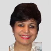
Nandini Tandon
Co-Founder of Silicon Valley based VC in HealthTech
IndUS Setu Global Foundation
Jami Mei
VP of Business Development
Arizona Commerce Authority
Douglas E. Kiehl
Sr. Vice President
BioCrossroads
Mark Dydyk
Director of Engineering & Operations
Medtronic
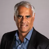
Fireside Chat: Harnessing Semiconductor For transformational Advancements in HealthTech
Abstract Moderator: Nandini Tandon Panelists: Jami Mei, VP of Business Development, Arizona Commerce Authority Douglas E. Kiehl, Sr. Vice President, BioCrossroads Mark Dydyk, Director of Engineering & Operations, Medtronic
Join us for a three-day workshop uniting FlexTech, NBMC, Smart MedTech, and the Medical Device Manufacturing Multiplier (MDM2) — a consortium of companies, institutions, and statewide organizations working to establish Greater Phoenix as a premier hub for medical device manufacturing. This collaborative event will drive innovation in electronics and medical technologies by bringing together industry leaders, innovators, and stakeholders.
The workshop will delve into advancements, challenges, and gaps in critical technologies such as flexible hybrid electronics, hybrid electronics, and bio-signal sensing for real-time cognitive and physical state monitoring and augmentation and will highlight the collaboration between the Smart MedTech Initiative and MDM2, focusing on the voice of the customer—clinicians and patients.
2025 Technology Workshop Shaping the Future of Advancing Electronics and Medical Technologies
- FHE Gap Analysis and NBMC Gap Analysis
- MDM2 and Smart Medtech Workshop
8:00 am - 6:00 pm
Off
Add to Calendar2025-04-22 08:00:002025-04-24 18:00:002025 Technology Workshops Shaping the Future of ElectronicsPresented By
Join us for a three-day workshop uniting FlexTech, NBMC, Smart MedTech, and the Medical Device Manufacturing Multiplier (MDM2) — a consortium of companies, institutions, and statewide organizations working to establish Greater Phoenix as a premier hub for medical device manufacturing. This collaborative event will drive innovation in electronics and medical technologies by bringing together industry leaders, innovators, and stakeholders.The workshop will delve into advancements, challenges, and gaps in critical technologies such as flexible hybrid electronics, hybrid electronics, and bio-signal sensing for real-time cognitive and physical state monitoring and augmentation and will highlight the collaboration between the Smart MedTech Initiative and MDM2, focusing on the voice of the customer—clinicians and patients. ASU Health Futures Center 6161 E Mayo Blvd Phoenix, AZ 85054 United StatesSEMI.org[email protected]America/Phoenixpublic
America/Phoenix
Register Now
This course offers a solid foundation in semiconductor manufacturing, from basic concepts to advanced techniques, providing practical insights into the tools, processes, and technologies driving the industry.
Learning Objectives
Gain a comprehensive understanding of the semiconductor industry and manufacturing process, design, and eco-system of the semiconductor industry
Understand the jargon, tools, and materials used in the design and fabrication of an integrated chip
Effectively be able to communicate semiconductor manufacturing concepts with other associates and industry professionals
Course Topics
Basic Electronics and Microelectronics: Definitions of essential electronic terms/concepts and introduction to microelectronics and integrated circuits
Process Nodes: Process nodes and their impact on device performance and cost
Device Physics and Transistor Operation: Principles of device operation and transistor functionality
Crystal Growth and Wafer Preparation: Crystal growth techniques and wafer preparation processes
Advanced Transistor Technologies: FDSOI, FinFETs, and Gate-All-Around (GAA) transistors and their impact on device performance
Circuit Design and Layout: Introduction to circuit design, layout techniques, and tools
Wafer Processing:
Mask Making and Lithography: Techniques and materials used in mask making and various lithographic methods (DUV, Immersion, EUV)
Clean Room Environments: Importance of clean rooms in semiconductor manufacturing and contamination issues
Etching and Cleaning Processes: Plasma and wet etching processes
Ion Implantation and Diffusion Techniques: Methods for doping and controlling diffusion in semiconductor fabrication
Deposition Techniques: RTP, CVD, ALD, and ALE techniques and their effect on device performance
Electroplating and Sputtering: Metal deposition techniques used in manufacturing
Packaging and Testing: Techniques such as wire bonding, die stacking, flip chip, and chiplets packaging, semiconductor testing processes
Metrology and Measurement Tools: Tools and methods used for precision measurement in semiconductor manufacturing
Semiconductor Industry Ecosystem: The major players in the industry
Who Should Attend
Anyone interested in understanding semiconductor manufacturing, including new employees, professionals in related industries, and those seeking to broaden their knowledge of the field.
Note that only the person who registered will receive a certificate of completion. This virtual training will not be recorded. Attendees must be present to access course knowledge.
Can't find the training link day of? After you register, you will receive the link to the live training via the email address you provided. In addition, you will receive email reminders about 24 hours in an advance and an hour before with the same link. Please keep these emails on hand to access the trainings on time. If you do not see any confirmation emails, please check your junk/spam folders before contacting SEMI U for support.
Holiday Inn (Portland West - Hillsboro) 2575 NE Aloclek Dr. Hillsboro, OR97124 United States
Gain a comprehensive understanding of the semiconductor industry and the integrated circuit (IC) manufacturing process. This course is designed for new personnel in the field or anyone seeking a well-rounded knowledge of the tools, materials, and terminology used in semiconductor manufacturing.
Pricing
Early Bird Special! $100 off until April 29th.
Members:$1,295 $1,195
Non-Members:$1,395 $1,295
* For group orders with 10+ attendees, and for Students/Veterans discounted pricing, please contact [email protected].
Overview of Semiconductor Manufacturing
In-Person Training
8:30 am - 5:00 pm
Off
Add to Calendar2025-05-13 08:30:002025-05-14 17:00:00Overview of Semiconductor Manufacturing (Portland, OR) Gain a comprehensive understanding of the semiconductor industry and the integrated circuit (IC) manufacturing process. This course is designed for new personnel in the field or anyone seeking a well-rounded knowledge of the tools, materials, and terminology used in semiconductor manufacturing.PricingEarly Bird Special! $100 off until April 29th. Members: $1,295 $1,195Non-Members: $1,395 $1,295* For group orders with 10+ attendees, and for Students/Veterans discounted pricing, please contact [email protected].Holiday Inn (Portland West - Hillsboro) 2575 NE Aloclek Dr. Hillsboro, OR 97124 United StatesSEMI.org[email protected]America/Los_Angelespublic
America/Los_Angeles
Register Now
Agileo Automation Launches The E84 PIO Box For The Enhanced Compliance Testing Of Semiconductor Equipment With SEMI Standards
Innovative plug-and-play device helps conduct comprehensive equipment compliance tests for automatic carrier delivery in automated fabs
SEMICON Europa, Munich, Germany, November 12, 2024 – Agileo Automation, a leading provider of control and connectivity solutions for global semiconductor equipment manufacturers, today launches the E84 PIO Box at Booth #C2848. This handheld device offers a new lightweight interface for fab staff to test semiconductor equipment software for compliance with SEMI’s E84 and GEM300 standards suite for automatic carrier delivery. It improves the readability, identification, and validation of E84 signal exchanges and functional aspects in cleanrooms or workshops. Integrated with Agileo Automation’s Speech Scenario software that emulates the fab host and validates the SECS/GEM interface with predefined test scenarios, the E84 PIO Box can easily emulate automated carrier delivery systems such as overhead hoist transport or automated guided vehicles. It is able to detect non-compliance and other functional issues thanks to its close alignment with SEMI’s E84 standard. The device features a DB25 connector for easy integration with E84 passive systems such as a load port and connects directly to a PC via a single USB cable for both data and power supply.
“In highly automated fabs, even minor carrier delivery issues can lead to costly downtime. Our E84 PIO Box is designed to rigorously validate nominal and error cases, ensuring seamless operations and fast recovery, benefiting both equipment manufacturers and facilities alike,” explains Marc Engel, CEO of Agileo Automation. “Early adopters have seen significant improvements in overall equipment software quality and now approach each software update with greater confidence, backed by consistent testing results.”
About Agileo Automation
Since its inception in 2010 in Poitiers, France, Agileo Automation has empowered global semiconductor equipment manufacturers to optimize their production machines with control, communication, data acquisition, and testing solutions, enabling their deployment in large-scale fabs worldwide. At the heart of Industry 4.0, Agileo’s A²ECF-SEMI framework provides a robust foundation for developing equipment controller software, leveraging the SEMI SECS/GEM and GEM300 standard suites. As a member of SEMI and the OPC Foundation, Agileo is a key contributor to the development and integration of industry standards such as SEMI standards and OPC Unified Architecture (OPC-UA). For more information, please visit our web site or follow us on LinkedIn.
PDF Solutions announces industry leaders speaking at its AI Executive Conference on Dec 12th, 2024, in San Francisco
PDF Solutions, Inc. (Nasdaq: PDFS), a leading provider of comprehensive data solutions for the semiconductor ecosystem, today announces the list of industry leaders speaking at its AI Executive Conference to be held on December 12th, 2024, in San Francisco, CA.
This event features keynotes, presentations, panels and demonstrations offering insights into the power of AI to transform semiconductor design and manufacturing. It includes talks on the state of art and best practices to design, deploy, scale and manage AI/ML solutions across the global semiconductor industry from PDF Solutions executives, other industry thought leaders, solutions experts and partners and users.
Three keynote presentations will look at how AI is currently being deployed in semiconductor manufacturing. Aziz Safa, Vice President and General Manager at Intel, will describe “How Analytics and AI are helping to transform a leading semiconductor company.” Smitha Mathews from ADI will discuss how semiconductor companies can “Get ready for AI” and the lessons learned from a real-life deployment. John Kibarian, PDF Solutions’ CEO will explain how AI is the next evolution of PDF Solutions portfolio.
Confirmed speakers include:
Aziz Safa Intel, VP and GM Analytics and Automation
Smitha Mathews Analog Devices, Senior Manager, Data & Analytics Strategy
Mike Campbell Qualcomm, Senior VP Engineering
Shyam Gooty Microsoft, Senior Director Product Engineering
Jean Philippe Fricker Cerebras, Founder and Chief System Architect
Anton Devilliers TEL, VP RnD
Jayant D’Souza Siemens, Principal Technical Product Manager
Marc Hunter Siemens, Director Product Management
Ken Butler Advantest, Senior Director Applications Marketing
Eli Roth Teradyne, Product Manager
Sunil Gandhi SAP, Sr Director Industry Executive, High Tech
Jason Schnitzer Yurts, CTO
Steve Mahoney Yurts, VP Product Management
Handel Jones International Business Strategies (IBS), founder and CEO.
Date: December 12, 2024
Following the 70th Annual IEEE International Electron Devices Meeting.
Location: St. Regis Hotel 125 3rd St San Francisco, CA 94103
About PDF Solutions
PDF Solutions (NASDAQ: PDFS) provides comprehensive data solutions designed to empower organizations across the semiconductor ecosystem to improve the yield and quality of their products and operational efficiency for increased profitability. The Company’s products and services are used by Fortune 500 companies across the semiconductor ecosystem to achieve smart manufacturing goals by connecting and controlling equipment, collecting data generated during manufacturing and test operations, and performing advanced analytics and machine learning to enable profitable, high-volume manufacturing.
Founded in 1991, PDF Solutions is headquartered in Santa Clara, California, with operations across North America, Europe, and Asia. The Company (directly or through one or more subsidiaries) is an active member of SEMI, INEMI, TPCA, IPC, the OPC Foundation, and DMDII. For the latest news and information about PDF Solutions or to find office locations, visit https://www.pdf.com/.
By focusing on the basics of each processing step and the issues surrounding them, participants will learn why certain techniques are preferred over others. Our instructors work hard to explain how semiconductor processing works without delving heavily into the complex physics and mathematical expressions that normally accompany this discipline.
Participants learn basic but powerful aspects about the semiconductor industry. This skill-building series is divided into three segments:
1. Basic Processing Steps. Each processing step addresses a specific need in IC creation. Participants learn the fundamentals of each processing step and why they are used in the industry today.
2. The Evolution of Each Processing Step. It is important to understand how wafer fab processing came to the point where it is today. Participants learn how each technique has evolved for use in previous and current generation ICs.
3. Current Issues in Wafer Fab Processing. Participants learn how many processing steps are increasingly constrained by physics and materials science. They also learn about the impact of using new materials in the fabrication process and how those materials may create problems for the manufacturers in the future.
Learning Objectives
Review of the semiconductor industry and its technical issues.
Understand the basic concepts behind the fundamental wafer fab processing steps.
Identify the key issues related to each of the processing techniques and their impact on the continued scaling of the semiconductor industry.
Identify the basic features and principles associated with each major processing step. These include processes like chemical vapor deposition, ion implantation, lithography, and etching.
Understand how processing, reliability, power consumption and device performance are interrelated.
Make decisions about how to construct and evaluate processing steps for CMOS, BiCMOS, and bipolar technologies.
Who Should Attend
This course is a must for every manager, engineer and technician working in the semiconductor industry, using semiconductor components or supplying tools to the industry.
Note that only the person who registered will receive a certificate of completion. This virtual training will not be recorded. Attendees must be present to access course knowledge.
Can't find the training link day of? After you register, you will receive the link to the live training via the email address you provided. In addition, you will receive email reminders about 24 hours in an advance and an hour before with the same link. Please keep these emails on hand to access the trainings on time. If you do not see any confirmation emails, please check your junk/spam folders before contacting SEMI U for support.
Semiconductor and integrated circuit developments continue to proceed at an incredible pace. The industry as a whole has gotten to this point of incredible complexity through the process of countless breakthroughs and developments in wafer fab processing. Today’s wafer fab contains some of the most complex and intricate procedures ever developed by mankind. Wafer Fab Processing is a 8 hour course (across two days) that offers an overview look into the semiconductor manufacturing process, and the individual processing technologies required to make them. We place special emphasis on the basics surrounding each technique, and we summarize the current issues related to manufacturing the next generation devices.
Pricing
Members: $599
Non-Members: $649
Students/Vets: $549
* For group orders with 10+ attendees, and for Students/Veterans discounted pricing, please contact [email protected].
Wafer Fab Processing
Virtual Training - US & EU
8:00 am - 12:00 pm
Off
Add to Calendar2025-04-14 08:00:002025-04-15 12:00:00Wafer Fab Processing (Virtual Training, US & EU) Semiconductor and integrated circuit developments continue to proceed at an incredible pace. The industry as a whole has gotten to this point of incredible complexity through the process of countless breakthroughs and developments in wafer fab processing. Today’s wafer fab contains some of the most complex and intricate procedures ever developed by mankind. Wafer Fab Processing is a 8 hour course (across two days) that offers an overview look into the semiconductor manufacturing process, and the individual processing technologies required to make them. We place special emphasis on the basics surrounding each technique, and we summarize the current issues related to manufacturing the next generation devices. PricingMembers: $599Non-Members: $649Students/Vets: $549* For group orders with 10+ attendees, and for Students/Veterans discounted pricing, please contact [email protected].United StatesSEMI.org[email protected]America/Los_Angelespublic
America/Los_Angeles
Sold Out
This course offers a solid foundation in semiconductor manufacturing, from basic concepts to advanced techniques, providing practical insights into the tools, processes, and technologies driving the industry.
Learning Objectives
Gain a comprehensive understanding of the semiconductor industry and manufacturing process, design, and eco-system of the semiconductor industry
Understand the jargon, tools, and materials used in the design and fabrication of an integrated chip
Effectively be able to communicate semiconductor manufacturing concepts with other associates and industry professionals
Course Topics
Basic Electronics and Microelectronics: Definitions of essential electronic terms/concepts and introduction to microelectronics and integrated circuits
Process Nodes: Process nodes and their impact on device performance and cost
Device Physics and Transistor Operation: Principles of device operation and transistor functionality
Crystal Growth and Wafer Preparation: Crystal growth techniques and wafer preparation processes
Advanced Transistor Technologies: FDSOI, FinFETs, and Gate-All-Around (GAA) transistors and their impact on device performance
Circuit Design and Layout: Introduction to circuit design, layout techniques, and tools
Wafer Processing:
Mask Making and Lithography: Techniques and materials used in mask making and various lithographic methods (DUV, Immersion, EUV)
Clean Room Environments: Importance of clean rooms in semiconductor manufacturing and contamination issues
Etching and Cleaning Processes: Plasma and wet etching processes
Ion Implantation and Diffusion Techniques: Methods for doping and controlling diffusion in semiconductor fabrication
Deposition Techniques: RTP, CVD, ALD, and ALE techniques and their effect on device performance
Electroplating and Sputtering: Metal deposition techniques used in manufacturing
Packaging and Testing: Techniques such as wire bonding, die stacking, flip chip, and chiplets packaging, semiconductor testing processes
Metrology and Measurement Tools: Tools and methods used for precision measurement in semiconductor manufacturing
Semiconductor Industry Ecosystem: The major players in the industry
Who Should Attend
Anyone interested in understanding semiconductor manufacturing, including new employees, professionals in related industries, and those seeking to broaden their knowledge of the field.
Note that only the person who registered will receive a certificate of completion. This virtual training will not be recorded. Attendees must be present to access course knowledge.
Can't find the training link day of? After you register, you will receive the link to the live training via the email address you provided. In addition, you will receive email reminders about 24 hours in an advance and an hour before with the same link. Please keep these emails on hand to access the trainings on time. If you do not see any confirmation emails, please check your junk/spam folders before contacting SEMI U for support.
Norris Conference Center 2525 W Anderson Ln. #365 Austin, TX78757 United States
Gain a comprehensive understanding of the semiconductor industry and the integrated circuit (IC) manufacturing process. This course is designed for new personnel in the field or anyone seeking a well-rounded knowledge of the tools, materials, and terminology used in semiconductor manufacturing.
Pricing
Members: $1,195
Non-Members: $1,295
* For group orders with 10+ attendees, and for Students/Veterans discounted pricing, please contact [email protected].
Overview of Semiconductor Manufacturing
In-Person Training
8:30 am - 5:00 pm
Off
Add to Calendar2025-04-29 08:30:002025-04-30 17:00:00Overview of Semiconductor Manufacturing (Austin, TX) Gain a comprehensive understanding of the semiconductor industry and the integrated circuit (IC) manufacturing process. This course is designed for new personnel in the field or anyone seeking a well-rounded knowledge of the tools, materials, and terminology used in semiconductor manufacturing.PricingMembers: $1,195Non-Members: $1,295* For group orders with 10+ attendees, and for Students/Veterans discounted pricing, please contact [email protected].Norris Conference Center 2525 W Anderson Ln. #365 Austin, TX 78757 United StatesSEMI.org[email protected]America/Chicagopublic
America/Chicago
Sold Out