Off
Add to Calendar2025-03-26 00:00:002025-03-26 00:00:00CDC Metaverse - Display on SiliconShanghai ChinaSEMI.org[email protected]America/Los_Angelespublic
Off
Add to Calendar2025-03-26 00:00:002025-03-26 00:00:00Advanced Material Conference(AMC)Shanghai ChinaSEMI.org[email protected]America/Los_Angelespublic
Compound Semiconductor Asia Conference (CS Asia) 2025
-
Off
Add to Calendar2025-03-25 00:00:002025-03-27 00:00:00Compound Semiconductor Asia Conference (CS Asia) 2025Shanghai ChinaSEMI.org[email protected]America/Los_Angelespublic
Heterogeneous Integration (Advanced Packaging) International Conference (HIIC)
Off
Add to Calendar2025-03-25 00:00:002025-03-25 00:00:00Heterogeneous Integration (Advanced Packaging) International Conference (HIIC)Shanghai ChinaSEMI.org[email protected]America/Los_Angelespublic
SiC—Silicon Carbide Webinar #7
Registration
Member: $49 Non-Member: $99
Registrants will receive the presentation recording and PDFs of Webinar #7.
SiC Planar and Trench MOSFETs: Design, Fabrication, and Key Applications
Silicon Carbide (SiC) MOSFETs exploit the material’s favorable properties, which allow for highly efficient power devices with reduced form-factor and cooling requirements. Having been commercially introduced in 2011, SiC MOSFETs have gone through several generations of improvements and are currently offered in planar and trench configurations by major semiconductor chip manufacturers. This webinar will provide an impartial overview of planar/trench design and fabrication aspects, highlight their key competitive advantages, and provide an independent overview of what real-world converters require in terms of application-specific performance parameters. Exemplary applications to be discussed include aviation, servo drivers, energy storage, and traction drives.
View other webinars in the SiC Series
Webinar #1—Silicon Carbide Material Properties, Key Applications, and Fabrication Basics: Making the Transition from Silicon
Webinar #2—Non-CMOS Compatible SiC Power Device Fabrication in Volume Si Fabs
Webinar #3—Bidirectional SiC and GaN Switch Technology
Webinar #4—Understanding SiC Chip Cost, the Impact of Defects, and the Case of Price Parity with Si at the System Level
With the world's growing reliance on semiconductor chips, the industry needs a more reliable solution to improve and innovate at a rapid pace while addressing manufacturing challenges such as temperature, chemistry, and mechanical issues.
One critical equipment in the industry is vacuum Pendulum Valves, a vacuum equipment incorporating plasma that are widely used in the semiconductor manufacturing process. The form, fit and function of these valves pose multiple challenges for the seals required in the valve's assemblies. Greene Tweed engineers have analyzed the most commonly used pendulum valves and broken down the various sealing challenges and have also created solutions to the challenges.
Join us to learn about the 6 W's—Who, What, When, Where, Why, & How—of these pendulum valve solutions.
Who—Anyone running a vacuum plasma chamber, etch and/or deposition
What—The pendulum valves, specifically the seals in the valve
Where—Every fabricator in the world
When—Now, as there are, tens of thousands that are currently operating
Why—The prevalent sealing challenges for pendulum valves
How—The sealing solutions and how we develop them, and the case study behind it to show in the 'How' part as well
Join our webinar where Greene Tweed engineers will discuss the most commonly used pendulum valves, the various sealing challenges and solutions to address them.
United States
Virtual Webinar | Tuesday, March 4, 2025 | Pacific Time
Cancellations received on or before August 16, 2025 are fully refunded with a $100 processing fee. Refunds will not be issued for cancellations (including no-shows) made after August 16, 2025, and only substitutions are accepted with a written note from the registered attendee. Please email your cancellations or substitutions on company letterhead to:
SEMI is proud to partner with the following media and associations to bring you news about this event. Click below to read, subscribe, or visit their website to learn more about each of them.
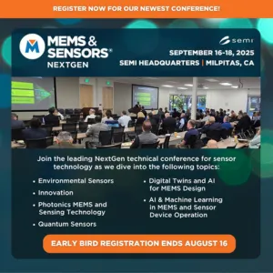
Speakers represent the MEMS and sensors supply chain and adjacent industries. The conference will explore cutting-edge topics including photonics, digital twins and AI, machine learning, environmental sensors, quantum sensors, entrepreneurialism, innovation and collaboration. The programming is curated to appeal to the “NextGen” MEMS and sensors professionals through programming features of the conference that include networking, problem-solving, and skill development.
TOPICS
Gain insights as we dive into the following topics:
Environmental Sensors
Innovation
Photonics MEMS and Sensing Technology
Quantum Sensors
Digital Twins and AI for MEMS Design
AI & Machine Learning in MEMS and Sensor Device Operation
WHO SHOULD ATTEND
This conference is open to all MEMS & sensors professionals interested in NextGen technology.
System Approach in Boosting Sensitivity, Selectivity, and Stability of Modern Environmental and Industrial Gas sensors to Deliver Broad Societal Impact
The Computer History Museum (CHM) is a computer museum in Mountain View, California. The museum presents stories and artifacts of Silicon Valley and the Information Age, and explores the computing revolution and its impact on society. Transportation will be provided.
MEMS & Sensors NextGen—MSNG 2025 is the leading NextGen sensor technology technical conference for NextGen professionals related to designing, building, and using sensors.
MEMS & Sensors NextGen 2025
September 16-18, 2025
SEMI HQ, Milpitas, CA
2:30 pm - 6:30 pm
Off
Add to Calendar2025-09-16 14:30:002025-09-18 18:30:00MEMS & Sensors NextGenMEMS & Sensors NextGen—MSNG 2025 is the leading NextGen sensor technology technical conference for NextGen professionals related to designing, building, and using sensors. SEMI HQ 673 South Milpitas Boulevard Seminars 1 & 2 Milpitas, CA 95035 United StatesSEMI.org[email protected]America/Los_Angelespublic
America/Los_Angeles
Sponsorships can be tailored to meet your branding and marketing objectives. Become a sponsor and brand your company at the Pacific Northwest Breakfast Forum.
Contact Tim Janes, [email protected] to learn about available sponsorship opportunities.
Powering the AI Era: Infrastructure, Integration & Policy
There has never been a more pivotal moment for the semiconductor industry. As AI adoption accelerates across every sector, the demands on infrastructure, technology integration, and policy frameworks have intensified. Companies across the Pacific Northwest and beyond are navigating rapid capacity expansion, new technical challenges, and the workforce transformation required to support the AI era.
This year’s SEMI Pacific Northwest Breakfast Forum brings together leaders from industry, government, academia, and regional organizations to explore how we build the resilient, intelligent, and scalable semiconductor ecosystem the AI future requires.
Join us as we examine energy infrastructurereadiness, advanced packaginginnovation, economic signals, and regional workforce development initiatives—all essential to powering the next decade of growth.
Intel - RA1 2501 NE Century Blvd Hillsboro, OR97124 United States
7:30 am
-
8:00 am
Check-In & Networking Breakfast
Host—Intel
8:00 am
-
8:05 am
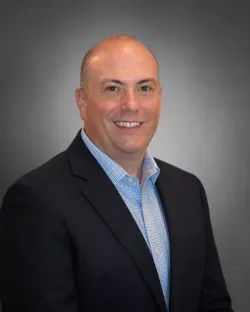
Damian Scandiffio
Co-Chair of SEMI Pacific Northwest Chapter
Acara Solutions
Matt Kleinke
Co-Chair of SEMI Pacific Northwest Chapter
Siltronic
SEMI Pacific Northwest Chapter Welcome Remarks
8:05 am
-
8:15 am
David Bloss
Corporate VP, Technology & Manufacturing Group General Manager, Global Sourcing for Equipment and Materials
Powering the AI Era: Infrastructure, Integration & Policy
SEMI Pacific Northwest Chapter
In-Person | April 30, 2026
7:30 am - 11:15 am
Off
Add to Calendar2026-04-30 07:30:002026-04-30 11:15:00Pacific Northwest Chapter Breakfast Forum—Powering the AI Era: Infrastructure, Integration & PolicyOrganizer: SEMI Pacific Northwest ChapterHosted by IntelIN-PERSONIntel - RA1 2501 NE Century Blvd Hillsboro, OR 97124 United StatesSEMI.org[email protected]America/Los_Angelespublic
America/Los_Angeles
2
The decisions made at the design stage of today's greenfield fabs will shape U.S. semiconductor performance for the next two decades. This webinar explores how organizations can move beyond traditional automation toward adaptive and ultimately autonomous fabs—starting with the foundational design of the built environment. Focusing on greenfield projects, Siemens experts will outline how early integration of power distribution, building systems, and automation technologies enables scalable, resilient, and future-ready facilities. Attendees will learn why designing autonomy requires a holistic approach—one that connects infrastructure, process, and production through a unified technology stack. The webinar will address challenges in adapting global fab designs to U.S. markets, highlighting the need for local expertise, regulatory alignment, and lifecycle planning. It will also explore how digitalization, predictive maintenance, and connected ecosystems drive efficiency in brownfield sites. Join the webinar and discover how to design facilities ready for autonomous, high-performance fabs.
Key takeaways: Shift from automation to autonomy starts with design Future fabs require rethinking the built environment upfront—not just layering automation later.
Early integration is critical for scalability and resilience Aligning power distribution, building systems, and automation from the start enables flexible, future-ready facilities.
A unified technology stack connects infrastructure to production Achieving autonomy depends on a holistic approach that links physical infrastructure, processes, and operations end-to-end.
Localization and lifecycle planning are key for U.S. fabs Adapting global designs requires navigating local regulations, leveraging regional expertise, and planning for long-term operations.
Digitalization drives performance across both greenfield and brownfield sites Technologies like predictive maintenance and connected ecosystems improve efficiency and enable continuous optimization.
This webinar is in collaboration with
United States
Virtual Webinar | Tuesday, August 25, 2025 | 11am Pacific Time
11:00 am
Ben Green
Senior Digitalization Consultant
Siemens Digital Industries
Matthew Hamilton
Semiconductor Market Leader
Siemens Smart Infrastructure
Opening Remarks
Early integration is critical for scalability and resilience
A unified technology stack connects infrastructure to production
Localization and lifecycle planning are key for U.S. fabs
Digitalization drives performance across both greenfield and brownfield sites
11:45 am
Q&A Session
12:00 pm
Closing Remarks
Ben Green
Ben Green is a Senior Digitalization Consultant at Siemens Digital Industries, where he leads strategic customer engagements focused on digital transformation and industrial innovation. He works with manufacturers to develop and execute digitalization strategies that integrate automation, control systems, and advanced software solutions. With nearly two decades of experience at Siemens, Ben has held a variety of customer-facing roles spanning sales, business development, and technical consulting. He previously led the Siemens Industrial Automation Solution Partner Program, collaborating with system integrators across the United States. Ben specializes in helping organizations define a clear vision for their digital future and translating that vision into practical, actionable steps that deliver measurable results. Ben holds a B.S. focused in Industrial Distribution from Texas A&M University.
Matthew Hamilton
Matthew Hamilton leads Siemens Smart Infrastructure's Semiconductor Vertical segment. A mechanical engineer by training, Matthew began his career in product development and manufacturing before spending a decade delivering complex energy and infrastructure programs at scale. His eight years at Siemens have centered on executive-level engagement with large-scale, mission-critical facilities where power resilience, decarbonization, and built-environment performance converge. His technical depth spans MV/LV power distribution, microgrid integration, solar and battery storage, central utility plants, building automation, fire and life safety, and enterprise digitalization — giving him a distinctive lens on how energy architecture and built-environment strategy shape fab performance, resilience, and the long path toward operational autonomy. Matthew holds a B.S. in Mechanical Engineering from the University of California Santa Barbara and an MBA in Finance from the Graduate School of Management at the University of California, Davis.
Register now to join the live webinar in collaboration with Siemens!
From Automated to Autonomous: Rethinking Fab Design for the Future
SIEMENS WEBINAR IN PARTNERSHIP WITH SEMI
11:00 am - 12:00 pm
Off
Add to Calendar Disabled
America/Los_Angeles
2
Register
Sponsorships can be tailored to meet your branding and marketing objectives. Become a sponsor and brand your company at the SEMI Arizona Breakfast Forum.
Contact Tim Janes, [email protected] to learn about available sponsorship opportunities.
Host—
Playbook for Winning
Arizona’s semiconductor ecosystem is at an inflection point—poised to transform rapid growth into sustainable global leadership. This forum convenes industry executives, policymakers and innovators to define strategies for making Arizona the premier global semiconductor resource. The SEMI Arizona Breakfast Forum is where Arizona’s semiconductor current and future playbook is defined, designed to mobilize leadership towards actionable strategies helping evolve Arizona’s semiconductor industry into an international winning playbook.
Arizona’s Rapid Rise as America’s Semiconductor Headquarters has attracted major global companies, with more than 60 expansions and over $200 billion in new investments since 2020, including TSMC, Intel, and ASM, all of whom are expanding operations or building new fabs in AZ due to strong business climate, strategic location and infrastructure. Statewide commitment through the Arizona Semiconductor Task Force, and the National Semiconductor Economic Roadmap (NSER) are enhanced by targeted incentives to attract companies and federal-state-industry alignments reinforce Arizona as a national leader in the next era of US semiconductor sovereignty.
Join Us at Edwards Vacuum's Facility in Chandler to Learn More About—
Building the Premier Semiconductor Hub
Powering the Ecosystem—Infrastructure as the Foundation
The right strategy is critical to success. Arizona’s must include water reliability, energy stability, long-term sustainability and cost-competitiveness. The game plan must include sustainable growth at the scale demanded by advanced nodes, packaging and AI-driven manufacturing.
Leading Regional & Global Supply Chain Resilience
Developing a World-Class Talent Team
Executive Panel Discussion—Investing in the Future: Capturing Long Range Goals
Questions?
Karen Popp—Sr. Program Manager, Programs & Committees [email protected]
Edwards Vacuum 2411 E. Germann Rd. Chandler, AZ95286 United States
Arizona is evolving from rapid expansion to ecosystem integration, ensuring every piece of the value chain connects efficiently. All the fundamental components, from research institutions to logistics and infrastructure partners to materials suppliers, packaging facilities to fabs are fundamental elements to this integration.
9:10 am
-
9:40 am
Kathryn Sorensen, PhD
Director of Research & Professor of Practice, Kyl Center for Water Policy at Morrison Institute;
Senior Global Futures Scientist, Arizona State University
Powering the Ecosystem—Infrastructure as the Foundation - Water Resources
Arizona is leading the way in becoming the most resilient, efficient semiconductor hub in North America. Through diversified sourcing, regional collaboration, logistics optimization, and flexible, shock-resistant supply models, Arizona will lead the way. Deployment of automated mitigation workflows, enabling alternate-site activation and faster recovery. Strong emphasis on transparent supplier collaboration, including exchange of validated data across tiers down to parts and materials.
Arizona’s strategic success depends upon its ability to produce, attract, and retain top-tier semiconductor talent. This plan includes investment in semiconductor training programs, securing next-gen engineering talent, research partnerships, on-the-job R&D exposure, and providing retraining and upscaling pathways.
Investment in semiconductor training programs, securing next-gen engineering talent, research partnerships, on-the-job R&D exposure, and providing retraining and upscaling pathways.
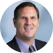
Vice President, Architecture, Advanced Design and Customer Enabling, Technology Development
Intel
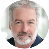
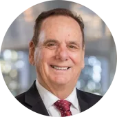
Richard Simoncic
Chief Operating Officer
Microchip Technology
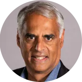
Nasser Peyghambarian, PhD
Professor of Optical Sciences and Materials Science and Engineering
University of Arizona
Executive Panel Discussion: Investing in the Future—Capturing Long Range Goals
The winning strategy will continue to require accelerated investments in R&D, creating new labs and testing capabilities, advanced packaging pilot lines, next-gen university research facilities, and sustainable infrastructure. Arizona is positioned to attract investments and to remain a market leader in 2026, 2030, and beyond.
SEMI Breakfast Forum Organized by SEMI Arizona Chapter
In-Person | Arizona Time
Arizona Breakfast Forum
In-Person | May 6, 2026
7:30AM–12:30PM Arizona Time
7:30 am - 12:30 pm
Off
Add to Calendar2026-05-06 07:30:002026-05-06 12:30:00SEMI Arizona Breakfast ForumSEMI Breakfast Forum Organized by SEMI Arizona ChapterIn-Person | Arizona TimeEdwards Vacuum 2411 E. Germann Rd. Chandler, AZ 95286 United StatesSEMI.org[email protected]America/Los_Angelespublic
America/Los_Angeles
2