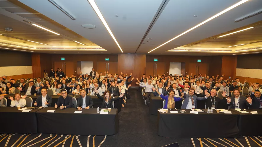
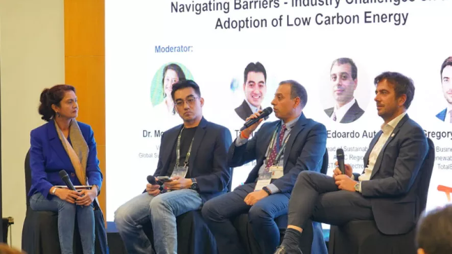
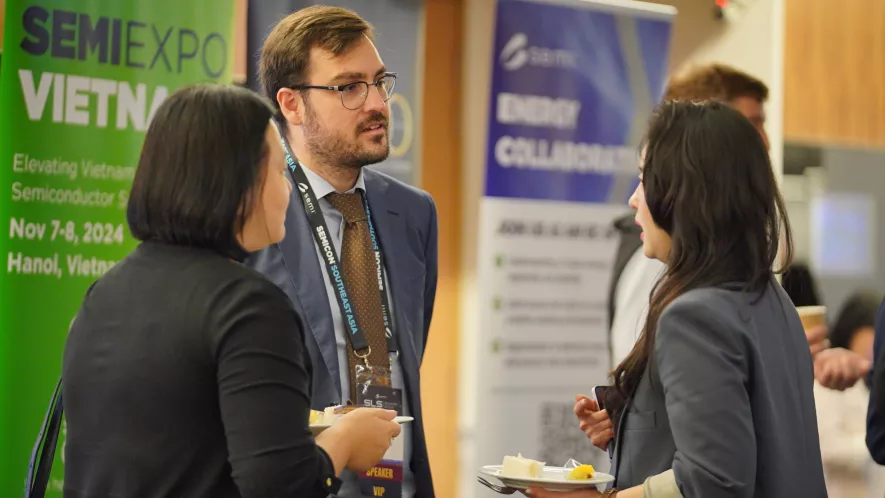
The summit will focus on the semiconductor industry's transition to renewable energy, bringing together leaders, policymakers, and experts to discuss its role in sustainable growth. Key topics include reducing carbon footprints, collaboration across the supply chain, and innovative solutions for achieving net-zero emissions. This initiative aims to strengthen the region's commitment to sustainability and position its semiconductor industry as a leader in green innovation and decarbonization.
1:30 pm - 5:30 pm
Off
Add to Calendar2024-10-10 13:30:002024-10-10 17:30:00SLS - SG Edition 2024Sustainability Transition: Collaboration - Innovation - TransitionThe summit will focus on the semiconductor industry's transition to renewable energy, bringing together leaders, policymakers, and experts to discuss its role in sustainable growth. Key topics include reducing carbon footprints, collaboration across the supply chain, and innovative solutions for achieving net-zero emissions. This initiative aims to strengthen the region's commitment to sustainability and position its semiconductor industry as a leader in green innovation and decarbonization.Meeting Room 300 - 301, Suntec Singapore Convention & Exhibition Centre 1 Raffles Boulevard Singapore 039593 SingaporeSEMI.org[email protected]Asia/Singaporepublic
Asia/Singapore
Register Now
Sponsoring the SEMI Silicon Valley Breakfast Forum offers unique opportunities to elevate your brand, connect with industry leaders, and influence the future of semiconductor innovation.
Contact Tim Janes, [email protected] to learn about available sponsorship opportunities.
Data Centers, Eat Your Vegetables: Building Sustainable Foundations for the AI Era
The industry has been feasting on AI growth, performance, and scale, but now must focus on the less glamorous necessities—efficiency, sustainability, materials, power, water, circularity, and supply chain resilience.
The AI boom has created unprecedented demand for compute, power, cooling, advanced materials, and infrastructure. While industry attention has focused on performance and scale, the next phase of growth will require discipline around resource efficiency, environmental impact, and long-term resilience. What are the "vegetables" the industry needs to consume today to ensure healthy growth tomorrow?
SEMI HQ 673 S. Milpitas Blvd. Milpitas, CA95035 United States
Thursday, November 5, 2026 | Pacific Time
7:00 am
-
8:00 am
Registration and Breakfast
8:00 am
-
8:10 am
Joe Stockunas
President
SEMI Americas
Welcome Remarks
8:10 am
-
8:20 am
Charlie Polidoro
Silicon Valley Co-Chair
Inventec
Introduction
8:20 am
-
9:20 am
Keynote Presentation
9:20 am
-
9:50 am
The AI Diet—Why Broccoli Matters More than Ever
9:50 am
-
10:20 am
The Energy Plate—Powering Growth Without Breaking the Grid
10:20 am
-
10:50 am
Hidden Ingredients—Which Resources will Become the Industry’s Biggest Bottleneck Over the Next Decade?
10:50 am
-
11:20 am
Networking Break
11:20 am
-
11:50 am
Healthy Growth—Sustainability to Business Imperatives
11:50 am
-
12:20 pm
Panel Discussion—From Chips to Chillers: The Sustainable Materials Stack Behind AI
12:20 pm
-
12:30 pm
Janell Centers
Marketing Manager
Macquarie
Closing Remarks
Presented by the SEMI Silicon Valley Chapter
Silicon Valley Breakfast Forum
November 5, 2026 | 7:30am–12:30pm | Pacific Time
7:30 am - 12:30 pm
Off
Add to Calendar2026-11-05 07:30:002026-11-05 12:30:00SEMI Silicon Valley Breakfast Forum Presented by the SEMI Silicon Valley Chapter SEMI HQ 673 S. Milpitas Blvd. Milpitas, CA 95035 United StatesSEMI.org[email protected]America/Los_Angelespublic
America/Los_Angeles
2
Convention Hall 3, 3F, Suwon Convention Center South Korea
9:00 am
-
9:30 am
Dae-Woo Kim
Samsung Electronics
The Journey of Semiconductor Industry and the Innovation of Advanced Packaging
Competition in the semiconductor industry is becoming fiercer and advanced package technology has become important for achieving low-power and high performance computing. As the Moore’s law reach the limitation, Si fabrication process need extremely high cost solutions such as multiple patterning and EUV (Extreme Ultra-Violet) lithography. In spite of high cost Si fabrication process, chip size is increased over the reticle size limit by adding more and more functional blocks for high performance computing. In particular, with the continuous demand for higher performance and capacity in memory products, the amount of data created, processed, stored and transferred is increasing tremendously. In order to overcome these challenges, advanced package based on RDL (Re-Distribution Layer), flip chip bonding, and TSV (Through Silicon Via) have been actively used for heterogeneous integration in electronic packages since the past decade. The heterogeneous integration and chiplet has been attracting a lot of attention since it enables higher bandwidth with low power consumption at reduced cost. 2.5D Si interposer architecture has been widely used for horizontal interconnection between logic to logic and logic to high bandwidth memory integration. 3D stacking architecture is for vertical interconnections enabling small form factor, increasing signal speed, reducing power consumption and power dissipation. In this talk, recent advanced package technology and key roadmap in Samsung Electronics will be shared for mobile and AI/HPC product.
Co-Process and Co-Development to Address Challenges in Co-Packaged Optics (CPO)
Co-Packaged Optics is the combination of photonic integrated circuits and electronic circuits at a system packaging level. The essential need is to get light in and out of the system, usually from optical fibers, with the least losses and ease of manufacturing. Photonic integrated circuits (PICs) are fabricated in CMOS semiconductor fabrication facilities, which allows manufacturers to take advantage of the large installed base of tools and processes. However, electronic packaging is currently not equipped to handle the challenges associated with packaging advanced photonic devices. In this presentation we explore some of these challenges for optical coupling such as sub-micron alignment tolerances, sensitivity to temperature variations, optical losses, and a lack of standards. The end objective is to have optical coupling look like electronic coupling. At NYCREATES/AIM Photonics, we have learned that the best results are obtained when the PIC manufacturing and packaging processes are co-designed to better achieve low-loss coupling, particularly between photonic integrated circuits and other elements in the system. A complete “end-to-end” approach includes customizing the PIC process, wafer manufacturing including interposers and heterogeneous integration, electronic photonic design automation, and electronic-photonic test, assembly and packaging capabilities. A complete approach will lead to reliable and affordable solutions that will ensure the manufacturing-readiness of this critical technology for decades to come.
Advanced Packaging Technology for HBM and 2.5D SiP
Rapid growth of generative AI at this moment has never been experienced for a few decades and it makes surprising impact to human experience and semiconductor industry as well. High bandwidth memory (HBM) which started from memory solution for high-end graphic applications has being emerged as a key driver accelerating the growth of AI industry due to remarkable advantages on the smaller latency between memory and GPU.
SK hynix has been the pioneer of HBM in all of history and firstly wrote a new record by the world-first development of HBM package in 2013. More remarkable footprint in the HBM history was the world-first adoption of the mass reflow bonding and molded underfill (MR-MUF) technology to the HBM 4Hi and 8Hi in 201, which nobody has never tried due to its notorious difficulties of process and material technologies. In this effort, SK hynix is providing a state-of-the-art of HBM products with highest memory bandwidth and memory capacity, highest power efficiency, and superior thermal dissipation ability and its package technology is a core competency leading the memory renaissance in the post-pandemic era.
In align with HBM technology innovation, there are continuous changes in 2.5D system-in-package (SiP) in order to improve the memory bandwidth and accommodate higher memory capacity. There has been many different types of proxy package structure to assure the HBM quality and reliability but it is obviously not certain whether HBM package can guarantee all the possible quality and reliability risks due to many possible changes of HBM and SiP packages in the future. In this paper, we would like to introduce several ways to evaluate the thermal and electrical characteristics of HBM and its package reliability.
The AI era has arrived and to enable and perpetuate it, the semiconductor advanced packaging (AP) industry needs to innovate in a torrid pace to keep in tandem the exponential growth of the Gen AI computing power.
Rising to the challenge, ASMPT has been leveraging its first mover market position in advanced packaging to continue innovating its end-to-end solutions to scale with the latest packaging architecture with the most demanding chiplet interconnects and heterogeneous integration formats.
Going forward, the AP industry shall undergo a “Power of N” transformation where interconnect pitch shall shrink rapidly along with thinner and bigger package formats, demanding new technologies in materials, process and equipment signaling a need for a complete and robust ecosystem to evolve for Gen AI to continue scaling.
As artificial intelligence (AI) continues to advance, the demand for high-performance computing has never been greater. Advanced packaging technologies play a pivotal role in meeting these demands by enhancing the performance, power efficiency, and integration density. This presentation explores the impact of various advanced packaging solutions, including 2.5D with Si interposers, 2.3D with RDL interposers, and 3D packaging technologies, on the development and optimization of AI systems.
We will delve into the specifics of 2.5D packaging, where Si interposers enable the integration of heterogeneous dies side by side, allowing for high-bandwidth communication and reduced latency. The presentation will also cover 2.3D packaging with RDL interposers, which offer a cost-effective alternative by utilizing advanced RDL processes to achieve similar benefits as 2.5D, but with potentially lower manufacturing complexity and cost.
Furthermore, we will examine 3D advanced packaging technology, which stacks dies vertically to further enhance integration density and performance. This approach not only maximizes space efficiency but also minimizes interconnect lengths, leading to significant improvements in speed and power consumption which are critical factors for AI applications.
Through a comprehensive analysis, this presentation will highlight how these advanced packaging technologies contribute to the acceleration of AI innovation, enabling more powerful, efficient, and compact AI packaging solutions.
Big data, artificial intelligence (AI), and high-performance computing (HPC) underscore the critical importance of advanced packaging technologies. Over the past decade, significant progress in 2.5D and 3D heterogeneous integration has led to notable improvements in I/O capacity, performance, cost efficiency, power consumption, and signal speeds for large-scale data processing.
In particular, 2.5D semiconductor packaging technologies such as EMIB and CoWoS are crucial for increasing I/O connections while reducing the interconnect length between logic and memory components, thereby enhancing performance and reducing latency.
However, FCBGA substrates used in AI/HPC packaging face considerable technical challenges. These substrates often need to be larger than 100mm x 100mm and consist of more than 20 layers. Furthermore, incorporating advanced technologies like silicon capacitor embedding and bridge integration into large-body FCBGA substrates presents additional hurdles as the industry moves towards next-generation packaging solutions.
This presentation thoroughly explores the latest technology trends in FCBGA substrates.
As the demand for higher performance, greater miniaturization, and improved thermal management continues to grow in the electronics industry, advanced packaging technologies are becoming increasingly critical. Glass substrates are emerging as a key material in this domain, offering unique advantages over conventional organic and silicon-based substrates. This talk explores the present and future potential of glass substrates in advanced packaging, focusing on their electrical, thermal, and mechanical properties that make them suitable for next-generation semiconductor devices.
It will also highlight recent innovations in glass substrate manufacturing, such as through-glass vias (TGVs) and surface modification techniques, which enhance the performance and reliability of electronic components.
Semiconductor Integration & Packaging: Powering AI and HPC The Advanced Packaging Summit is a conference dedicated to exploring the latest advancements in packaging technology for high-performance computing (HPC) and AI. The summit brings together leading experts, researchers, and industry professionals to share their insights and experiences on advanced packaging solutions that enable powering AI and HPC systems. Topics covered at the summit include 2.5D packaging, Chiplet packaging, CPO, FCBGA substrate technology and more. Attendees will gain valuable insights and have the opportunity to network with experts in the industry.
Advanced Packaging Summit 2024
9:00 am - 5:30 pm
Off
Add to Calendar2024-09-11 09:00:002024-09-11 17:30:00Advanced Packaging Summit 2024Semiconductor Integration & Packaging: Powering AI and HPCThe Advanced Packaging Summit is a conference dedicated to exploring the latest advancements in packaging technology for high-performance computing (HPC) and AI. The summit brings together leading experts, researchers, and industry professionals to share their insights and experiences on advanced packaging solutions that enable powering AI and HPC systems. Topics covered at the summit include 2.5D packaging, Chiplet packaging, CPO, FCBGA substrate technology and more. Attendees will gain valuable insights and have the opportunity to network with experts in the industry. Convention Hall 3, 3F, Suwon Convention Center South KoreaSEMI.org[email protected]America/Los_AngelespublicDiscover APS 2025
From Concept to Reality: Advancing Digital Twins in Semiconductor Manufacturing
Following up on the SEMI Digital Workshop 2023, this workshop will delve into the practical aspects of implementing digital twin technology in semiconductor manufacturing. The aim is to bridge the gap between theoretical concepts and real-world applications, providing participants with actionable insights and strategies to successfully develop and integrate digital twins into their operations. Further the workshop aims to address some of the future upcoming challenges in the areas of integration of multi-modal real time data sources, security, process complexity, scalability, and standards.
SEMI HQ 673 S Milpitas Blvd. Milpitas, CA95035 United States
Morning, Day 1: December 4, 2024
8:00 am
-
9:00 am
Registration & Breakfast
9:00 am
-
12:30 pm
Session #1 - Data Needs for Digital Twins - Data Sources, Integration & Interoperability
This session will explore the critical data requirements for creating and maintaining digital twins. Integrating multi-modal data sources (sensors, enterprise systems, equipment, etc.) that feed into digital twins, ensuring that they accurately reflect their physical counterparts is a minimum necessity. This session will also cover data integration techniques (from various factory systems), and interoperability to support dynamic digital twins.
9:00 am
-
9:10 am
Mark da Silva
Senior Director, Smart Manufacturing
SEMI
Welcome Remarks
9:10 am
-
9:35 am
Michael Neel
Director of Marketing
Inficon
Keynote - Enabling Autonomous Operations Through Integrated Digital Twins
9:35 am
-
10:00 am
Robert Baseman
Senior Technical Staff Member
IBM
Semantic Models for Microelectronic Manufacturing & Development
10:00 am
-
10:25 am
David McKee
Technology Leader & Managing Partner
Counterpoint Tech/DTC
Journey to Twins: A toolkit for Capabilities & Data to Digital Twins
10:25 am
-
10:40 am
Coffee Break - Sponsored by INFICON
10:40 am
-
11:05 am
Rad Desiraju
Director, WW Industry Advisory
Microsoft
Overcoming Data Interoperability Challenges for Effective Digital Twins
11:05 am
-
11:30 am
Wei Zhao
Head of Process Integration
Athinia
Chris Han-Adebekun
VP, Business Development
Athinia
Building Process & Supply Chain Digital Twins through Integrated Data Assets and Secure Data Sharing
11:30 am
-
12:30 pm
Dave Henshall
Vice President of Business Development and Government Relations
Semiconductor Research Corporation
Chris Ritter
CTO
Idaho National Lab
Special Session - SmartUSA – Semiconductor Digital Twin Manufacturing USA Institute
12:30 pm
-
2:00 pm
Lunch
Afternoon, Day 1: December 4, 2024
2:00 pm
-
5:00 pm
Session #2 - Data Standards for Digital Twins: Managing Unclean Factory Data
This session will focus on the importance of data standards for digital twins in semiconductor manufacturing, particularly in the context of dealing with unclean factory data. It will explore the challenges associated with unclean data and discuss strategies for cleaning and standardizing to ensure seamless ingestion into digital twins at various levels. Best practices for data validation, transformation, and integration as well as how to implement robust data standards to enhance reliability and accuracy of digital twins.
Sponsored by - Seeq
2:00 pm
-
2:25 pm
Dr. Joseph Ervin
Product Line Head of Semiverse Solutions Group
Lam Research
Keynote - Addressing Future Challenges in the Stochastics Era of Patterning with EUV Dry Resist
New patterning technologies will be needed to advance the device roadmap to 2 nm and beyond. Minimum pitch scaling will be exceptionally difficult to achieve at these advanced nodes, even with EUV patterning. Stochastic effects using wet resists during EUV patterning become problematic at the nanoscale, and can lead to line collapse, bridging, unacceptable line edge roughness (LER) and line width roughness (LWR). These stochastic effects present challenges when optimizing the tradeoffs between EUV resist resolution, dose, sensitivity, line edge / line width roughness, defectivity and cost.
In this talk, we will review the basics of dry resist technology, including dry resist equipment requirements, process flows and process integration modeling. In addition, we will present data that documents the advantages of dry resist technology over wet resist technology, demonstrating superior image quality, scaling and yield. We will conclude the talk by demonstrating a digital twin of the process integration and usage of optimization to achieve improved LER/LWR characteristics.
2:25 pm
-
2:50 pm
Alan Weber
Vice President, New Product Innovations
Cimetrix by PDF Solutions
Charting the Digital Twin Standardization Path: An Iterative Implementation and Abstraction Process
2:50 pm
-
3:15 pm
Brett Brimhall
Deloitte
3:15 pm
-
3:30 pm
Coffee Break - Sponsored by INFICON
3:30 pm
-
3:55 pm
Andres Torres
Engineer and Key Expert
Siemens
Feature Engineering as the bridge to Semantic Factory Data
3:55 pm
-
4:20 pm
Michael Bowcutt
Director of Sales Engineering for Romaric products at camLine
camLine USA
Control Software Integration with Digital Twins: How Virtual Data Aligns with Physical Reality
4:20 pm
-
5:20 pm
Moderator
Kenneth Smith
VP Growth Markets
Seeq
Sean Tropsa
Principal Analytics Engineer
Seeq
Panel: Harmonizing Standards for Semiconductor Digital Twins
5:30 pm
-
7:00 pm
Networking Reception - Sponsored by Sentient Cloud
Morning, Day 2: December 5, 2024
8:00 am
-
9:00 am
Registration & Breakfast
9:00 am
-
12:30 pm
Session #3 - Modeling High Complexity Semiconductor Processes
This session will explore the integration of digital twin technology in modeling high complexity semiconductor processes. As the semiconductor industry advances, the need for precise and efficient modeling techniques becomes crucial. Digital Twins offer a transformative approach to simulate and optimizes these processes, though challenges exist. Cases studies and future innovations will also be covered in this session.
9:00 am
-
9:05 am
Mark da Silva
Senior Director, Smart Manufacturing
SEMI
Welcome Remarks
9:05 am
-
9:30 am
Umesh Kelkar
Master/Vice President, Semiconductor Products Group
Applied Materials
Keynote: Key Enablers for Semiconductor Equipment and Process Digital Twins: Accelerated Computing (AC), Artificial Intelligence (AI) and Physics Modeling
9:30 am
-
9:55 am
Prith Bannerjee
Chief Technology Officer
Ansys
AI Driven Digital Twins for Semiconductor Manufacturing
9:55 am
-
10:20 am
Xi-Wei Lin
Executive Director, Applications Engineering
Synopsys
AI and Physics-based Models for Technological Development with High Complexity Semiconductor Processes
10:20 am
-
10:45 am
Coffee Break - Sponsored by PhysicsX
10:45 am
-
11:10 am
Amit Lal
Professor, Cornell University
Cornell
Peter Doerschuk
Professor
Cornell University
Ben Davaji
Assistant Professor
Northeastern University
Digital Twin Flow Using AI/ML Applied to Ferroelectric Memory
11:10 am
-
11:35 am
John Maculley
Semiconductor Industry Strategy Consultant
Dassault Systemes
Leveraging Virtual Twins and AI for Enhanced Fabrication Technology Co-Optimization in Semiconductor Manufacturing
11:35 am
-
12:30 pm
Pushkar Apte
Strategic Technology Advisor and Global Data-AI Lead
SEMI
Panel Discussion
12:30 pm
-
2:00 pm
Lunch - Sponsored by Dassault Systemes
Afternoon, Day 2: December 5, 2024
2:00 pm
-
5:00 pm
Session #4 - GenAI & AI/ML Role in the Development of Digital Twins - Implementation Strategies for DT
Integrating AI/GenAI & Digital Twins - Explore the cutting-edge integration of Generative AI (GenAI) and Artificial Intelligence/Machine Learning (AI/ML) in the creation and evolution of digital twins. This session will delve into how GenAI & AI/ML technologies are revolutionizing the simulation, prediction, and real-time replication of physical assets in semiconductors through case studies and practical applications.
2:00 pm
-
2:25 pm
Kamaljeet Ghotra
Senior Director, Go-To Market and Digital Strategy
PDF Solutions
Keynote - Accelerating Digital Twins with Gen AI
The rise of sophisticated AI tools, including generative AI, is revolutionizing the semiconductor industry by enabling the analysis of vast datasets to generate valuable insights. Executives in the sector see generative AI as a transformative force rather than just another tool. They believe it can deliver significant value, particularly in manufacturing, operations, and maintenance, its potential for process and equipment analysis, Predictive maintenance and smart diagnostics.
As fabs adopt smart manufacturing and virtual modeling it is pertinent for digital twins to leverage technologies like generative AI for data generation, Data Synthesis/Augmentation, Real Time Analysis, Model Optimization (AI enhanced physics models) , Rapid Prototyping and Accelerated Design and Development with data-driven model-based learning.
2:25 pm
-
2:50 pm
Peter Lendermann
CTO
D-SIMLAB
About Cross-Fertilization between Digital Twins and AI Techniques for Capacity Planning and WIP Flow Optimisation in Semiconductor Fabs
2:50 pm
-
3:15 pm
Kiran Karunakaran
Chief Technology Officer
Via Automation
Developing Explainable Digital Twins for the Semiconductor Industry Using GenAI, Knowledge Graphs, and ML Techniques
3:15 pm
-
3:30 pm
Coffee Break - Sponsored by PhysicsX
3:30 pm
-
3:55 pm
Mark Huntington
Managing Director of North America
PhysicsX
Real-Time Digital Twins for Semiconductor Manufacturing: Accelerating Multi-Physics Optimization with Physics-Based AI
3:55 pm
-
4:20 pm
Becky Kelderman
Solutions Sales Manager
Rockwell Automation
Advancing Industrial Data Architectures & Models for AI in Process Digital Twins
4:20 pm
-
5:20 pm
Moderator
Mithun Kamat
Partner
McKinsey
Panel - Rewiring organizations for AI / Digital twin: a business-backed view of successful implementation and challenges in adoption of Digital twins in the semiconductor industry
-
Following up on the SEMI Digital Workshop 2023, this workshop will delve into the practical aspects of implementing digital twin technology in semiconductor manufacturing. The aim is to bridge the gap between theoretical concepts and real-world applications, providing participants with actionable insights and strategies to successfully develop and integrate digital twins into their operations. Further the workshop aims to address some of the future upcoming challenges in the areas of integration of multi-modal real time data sources, security, process complexity, scalability, and standards.
Given the exclusivity and richness of discussions, please note that seats are capped at 80 attendees. Don’t wait to secure your spot.
From Concept to Reality: Advancing Digital Twins in Semiconductor Manufacturing
[IN-PERSON EVENT]
Dec 4-5, 2024
8:00 AM – 5:00 PM PT
8:00 am - 5:00 pm
Off
Add to Calendar2024-12-04 08:00:002024-12-05 17:00:00From Concept to Reality: Advancing Digital Twin in Semiconductor ManufacturingFollowing up on the SEMI Digital Workshop 2023, this workshop will delve into the practical aspects of implementing digital twin technology in semiconductor manufacturing. The aim is to bridge the gap between theoretical concepts and real-world applications, providing participants with actionable insights and strategies to successfully develop and integrate digital twins into their operations. Further the workshop aims to address some of the future upcoming challenges in the areas of integration of multi-modal real time data sources, security, process complexity, scalability, and standards. Given the exclusivity and richness of discussions, please note that seats are capped at 80 attendees. Don’t wait to secure your spot. SEMI HQ 673 S Milpitas Blvd. Milpitas, CA 95035 United StatesSEMI.org[email protected]America/Los_Angelespublic
America/Los_Angeles
Purchase On-Demand
INAUGURAL EVENT FOCUSED ON SMART MANUFACTURING & SMART MOBILITY
Join us for a groundbreaking Midwest conference and tradeshow on April 1-2, 2025, focused on Smart Manufacturing and Smart Mobility with an emphasis on the semiconductor industry! Automotive electronics and smart manufacturing are two of the key end markets on the path to $1T in semiconductor revenue.
A significant amount of both markets is concentrated in the Midwestern United States. SEMIEXPO in the Heartland will bring these two key markets together and provide an opportunity for collaboration and growth.
Smart Manufacturing
The program will focus on the deployment of Industry 4.0 or Smart Manufacturing tools, technologies, and methods for the semiconductors required for this growing market.
Smart Mobility
The program will unite stakeholders in the semiconductors/sensors and mobility ecosystems to identify and address technical issues and supply chain dynamics that are best addressed collectively.
Ways to Participate
Exhibit
Sponsor
Speak
Attend
MAKE YOUR MARK AT THE INAUGURAL SEMIEXPO HEARTLAND
Plan Now to Exhibit or Sponsor. Contact— Shane Poblete | +1 202-847-5983 | [email protected]
NEW EVENT!
April 1–2, 2025
Indiana Convention Center, Indianapolis, IN
Off
Add to Calendar2026-04-29 00:00:002026-04-30 00:00:00SEMIEXPO Heartland 2026Indiana Convention Center 100 S Capitol Ave Detroit, MI United StatesSEMI.org[email protected]America/Detroitpublic
America/Detroit
This webinar will introduce members of the military community to the semiconductor industry and connect them directly with veterans and recruiters. Employers recognize and need this skilled and talented community to join as the industry prepares for huge growth in the next few years. We will dive into the roles expected and qualifications needed to jump into an exciting new career. Opportunities nationwide!
About SEMI VetWorks
The SEMI VetWorks Initiative aims to address the microelectronics industry's need for attracting, developing, and retaining talent by tapping into the skills and experiences of military veterans and reservists. SEMI prioritizes connecting its members with this talented pool through initiatives that align industry hiring practices, internship, and apprenticeship programs. By leveraging existing training and credentialing opportunities, veterans gain access to well-paid technician and operator roles. The SEMI VetWorks Guidebook offers tools and recommendations for recruiting, hiring, and retaining veterans, while the SHRM Veterans at Work Certificate program provides additional resources for connecting with the military community.
Members of the Military Community, join us for an interactive and informative session about career opportunities in the semiconductor industry. Hear from employers and veterans in the industry directly!
SEMI VetWorks: Careers in Chips
The semiconductor industry needs your skills and experience!
Virtual Event #2
10:00am - 12:00pm PT, June 26th
10:00 am - 12:00 pm
Off
Add to Calendar2024-06-26 10:00:002024-06-26 12:00:00SEMI VetWorks: Careers in Chips Members of the Military Community, join us for an interactive and informative session about career opportunities in the semiconductor industry. Hear from employers and veterans in the industry directly!United StatesSEMI.org[email protected]America/Los_Angelespublic
America/Los_Angeles
Register Now
Your company has built a strong patent portfolio — now what? This webinar will discuss strategies for managing existing patents, including how to use IP to strengthen your business and maximize return on investment. Topics will include best practices for patent marking, controlling rising maintenance fees, and licensing, as well as insights into emerging trends in patent enforcement and litigation in the semiconductor sector.
ABOUT THE SPEAKER
Michael Jones, Partner, Rothwell Figg Michael H. Jones’s practice includes patent litigation, patent prosecution, and IP counseling. Michael advises clients who have developed a broad range of technologies, including semiconductor devices and manufacturing, integrated circuits and systems, green energy, terahertz electronics, hardware and protocols for wireless communications, and various online technologies. Although much of his work is with large multinational clients with complex patent portfolios, Michael also has a significant, and growing, practice with smaller high-technology clients, ranging from startups to growth companies dealing with patent issues for the first time in their evolution. Michael has a B.S. in Electrical and Computer Engineering from University of Virginia, a M.S. in Electrical and Computer Engineering from University of California, Santa Barbara, and a J.D. from The George Washington University Law School.
Best Practices for Semiconductor Patent Portfolio Management
Flexible Electronics Master Class #23
10:00 am - 12:00 pm
Off
Add to Calendar2024-11-06 10:00:002024-11-06 12:00:00FEMC #23 Best Practices for Semiconductor Patent Portfolio ManagementUnited StatesSEMI.org[email protected]America/Los_Angelespublic
America/Los_Angeles
Join this webinar to find out how companies across the semiconductor value chain are prioritizing employee-driven climate action and social impact,. Hear how employee-driven initiatives are enhancing sustainability and equity -- and gain ideas on how you and your organization might benefit.
With the Paris Climate Agreement and growing awareness of the climate crisis, many people are asking "how can I contribute in my private and professional life?"
This Employee Action Workshop, organized by the Climate Equity and Social Impact (CESI) workgroup of SEMI will focus on setting up sustainability-based employee groups within your company. How to engage speakers and attendees, and the resources that exist to help.
We will show you how to create an in-house, bottom-up sustainability network and offer concrete ideas for action. Industry leaders will share their experiences and successes, providing valuable insights into volunteerism, ESG innovation, and impactful employee initiatives.
For anyone who wants to use your biggest multiplier - your workplace - to make a difference in Climate Change.
This webinar takes place 8:00 AM - 9:00 AM Pacific Time Zone
How to Start & Grow an Employee Action Group for Sustainability
8:00 am - 9:00 am
Off
Add to Calendar Disabled
America/Los_Angeles
A high quality patent can turn an innovation into a valuable business asset. Strategic drafting of patent applications and the management of the prosecution of the application around the world is essential to obtaining maximum value. Learn how to ensure your valuable innovation remains protected while avoiding common pitfalls, including losing rights through errors like public disclosure or incomplete protection.
ABOUT THE SPEAKER
Brian Rosenbloom, Partner, Rothwell Figg With over two decades of experience in the intellectual property (IP) field and a strong technical background in the electrical and software arts, Rothwell Figg partner Brian Rosenbloom is an expert in patent prosecution, IP counseling, and patent litigation proceedings before the U.S. Patent and Trademark Office and in district courts across the country. Brian represents clients ranging from Fortune 100 companies to independent inventors, entrepreneurs, and emerging enterprises, and works with a broad range of technologies. Brian received a Bachelor’s degree in Electrical Engineering from Columbia University (Tau Beta Pi Engineering Honor Society, Eta Kappa Nu Electrical Engineering Honor Society), and worked as a software engineer at General Electric Information Services for several years. After working at GE, he pursued a law degree and received a J.D. from Georgetown University Law Center (cum laude).
How to Protect Your Valuable IP in the Microelectronics Industry
Flexible Electronics Master Class #22
10:00 am - 12:00 pm
Off
Add to Calendar2024-10-30 10:00:002024-10-30 12:00:00FEMC #22 How to Protect Your Valuable IP in the Microelectronics IndustryUnited StatesSEMI.org[email protected]America/Los_Angelespublic
The SEMI Supply Chain Management initiative is a unique global platform that brings together top industry leaders to advance a more resilient and agile electronics supply chain. Recent geopolitical and natural events have exposed vulnerabilities but also new opportunities that require industry-wide and precompetitive collaboration. That's where SEMI comes in. The initiative’s newly formed Industry Advisory Council is committed todriving engagement, creating tools and solutions through collaboration, and ensuring alignment in global end-to-end supply chain continuity, visibility, and transparency. Through deep dives, educational forums, benchmarking, standards development, and strategic partnerships, SEMI seeks to empower our members to anticipate and respond to future disruptions proactively.
If you are interested in learning more about how your company can participate in the SCM initiative, please contact us at [email protected].
Join us for an insightful webinar as we present the findings from the 2024 Semiconductor Supply Chain Survey, a collaborative effort between the SEMI Supply Chain Management initiative and McKinsey & Company.
The annual survey aims to establish benchmarks for operational agility metrics, covering the entire value chain from material suppliers to OEMs, offering a comprehensive view of the landscape.
During this webinar, we will share results from the survey uncovering key trends, challenges, and opportunities within the semiconductor supply chain. By attending, you'll gain valuable insights to benchmark your organization against peers, identify areas for improvement, and course-correct more effectively. Please contact us if you like to learn about how your company can participate in the SCM initiative.
Join us for a webinar on the 2024 Semiconductor Supply Chain Survey results, a collaboration between SEMI and McKinsey & Company. Discover key trends, challenges, and opportunities across the value chain. Gain insights to benchmark your organization and enhance your strategic planning.
Off
Add to Calendar2024-06-24 00:00:002024-06-24 00:00:00Benchmark Your Supply Chain AgilityJoin us for a webinar on the 2024 Semiconductor Supply Chain Survey results, a collaboration between SEMI and McKinsey & Company. Discover key trends, challenges, and opportunities across the value chain. Gain insights to benchmark your organization and enhance your strategic planning. Register now for one of the sessions:US/EU: 8:00 AM – 9:00 AM PT [Register Now] Asia: 5:00 PM – 6:00 PM PT [Register Now] United StatesSEMI.org[email protected]America/Los_Angelespublic