Worldwide, companies in the semiconductor value chain are undergoing paradigm shifts in how sustainable business is conducted, governed, and reported. From engineering to the board room, the number of interdependent corporate functions charged with improving corporate sustainability performance is growing rapidly, with implications for decision-making across the enterprise.
New global sustainability regulations mean that key decisions regarding a company's sustainability strategy can now have significant regulatory implications. Understanding how one decision affects (or forecloses) another is critical, and companies must think several steps ahead to put themselves in a position to achieve their sustainability objectives without painting themselves into a corner.
This webinar will focus on discrete examples where such an approach is paramount – including making climate risk materiality determinations, adopting a climate transition plan, making product-related sustainability claims, disclosing conflict minerals smelter names, and selecting a double materiality assessment methodology. For each example, we will leverage data to examine industry trends, identify the specific potential issues, and suggest practical strategies to navigate those issues.
To ground the conversation, we will illustrate various ways in which these issues can come up in practice by discussing a set of hypothetical sustainability decisions, the related regulatory implications, and approaches that balance sustainability objectives and regulatory considerations.
As the semiconductor industry prepares for the coming wave of new sustainability laws and regulations, companies have an opportunity to develop a regulatory strategy for sustainability that takes an integrated approach to regulatory requirements, encourages coordination and collaboration between the sustainability and legal departments, minimizes regulatory burden and compliance risk, and enables sustainable and responsible business. We will share common features of strategies that have been successful in this regard and provide our recommendations regarding operationalizing such a strategy in your organization.
This event inaugurates the SEMI webinar series, “Global State of Play: Sustainability Regulations, Reporting, & Incentives.” New in 2024, this series offers semiconductor industry professionals the chance to interact with top-tier experts on the most pressing challenges in compliance, disclosure, and strategy for sustainable business.
Speaker
Ashley Walter is Partner & Chief Sustainability Officer at Orrick, Herrington & Sutcliffe LLP, where he advises large technology companies, leading apparel brands, multinational retailers, and renewable energy project developers on business-critical climate, product sustainability, human rights and responsible sourcing issues. As Orrick’s Chief Sustainability Officer, he also oversees Orrick’s strategic sustainability initiatives.
Ashley focuses on developing innovative methods of supporting clients in achieving ESG objectives, including designing novel systems to manage supply chain risk; forming and guiding management-level ESG Steering Committees; and helping clients address the ESG requirements of major customers by engaging with those customers on his clients’ behalf.
Ashley is also heavily involved in ESG initiatives at Stanford Law School, where he has served as a moderator at the Stanford Directors’ College, has lectured on ESG at business law courses, and will be teaching the course “Law and Governance in ESG Strategy” in the spring of 2025.
Worldwide, companies in the semiconductor value chain are undergoing paradigm shifts in how sustainable business is conducted, governed, and reported. From engineering to the board room, the number of interdependent corporate functions charged with improving corporate sustainability performance is growing rapidly, with implications for decision-making across the enterprise.
Join us for this first event in our series, “Global State of Play: Sustainability Regulations, Reporting, & Incentives.” The series offers semiconductor industry professionals the chance to interact with top-tier experts on the most pressing challenges in compliance, disclosure, and strategy for sustainable business.
Times
Multiple sessions available!
EMEA: Monday, November 18, 2024 5:30-6:30 pm Central European Time (=8:30-9:30 am Pacific)
America: Monday, November 18, 2024 8:30-9:30 am or 4-5 pm Pacific Time
Asia Pacific: Tuesday, November 19, 2024 9-10 am Japan Standard Time (=4-5 pm Pacific)
Developing a Regulatory Strategy for Sustainability
Hours for Drop-off: 10:00 am - 3:30 pm (receipts available)
Lunch: 11:30 am - 12:30 pm
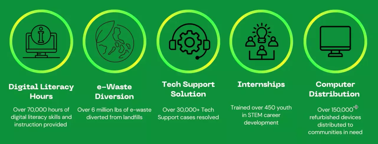
Program: 12:30 pm - 1:00 pm - Hear from Tech Exchange how the equipment will be refurbished and distributed and how recipients will receive the equipment, training and internet skills and access.
Tech Exchange's Highest Needs Current top priorities are laptops, desktops, and mini-computers. Other tech items are welcome, such as mice, keyboards, speakers, monitors, SSD drives, hard drives, cables, chargers, and networking equipment (including servers). All of these can be refurbished for use by students, families, or in classrooms.
In addition, we accept new or gently used tech accessories like laptop bags, tablet bags, and tech cases, as well as consumer technology such as Apple Watches, small speakers, digital/video cameras, audio equipment, drones, tablets, iPhones, iPads, and more.
All apple products that are donated must have their apple iCloud deactivated so we can reuse/repurpose it.
If an item is not on this list, please send Tech Exchange an email at [email protected].
For large lots (>100 laptops) please contact Tech Exchange to arrange a pick up at your location, visit Pickup.techexchange.org to schedule.
Together, we can help close the digital divide!
Join many other companies, including: SAP, Prospera, SmartZip, Snowflake, Sonic, Shell, Lonely Planet, Kaiser, Gap, ETrade, Benchmark Electronics, and many more.
Bring your decommissioned computer equipment to SEMI and change a life!
The SEMI Sustainability Climate Equity and Social Impact group is partnering with Tech Exchange to recycle, refurbish and reclaim your old or unusable computers and transform them into usable equipment for those without in the Bay Area. Tech Exchange secures the equipment, and then wipes all data from memory according to DOD standards, just like third-party e-waste firms do, and issues certificates as requested.
Drop off only, or join us for lunch and learn more about the program!
SEMI Members' Tech Donation Day
10:00 am - 3:30 pm
Off
Add to Calendar2024-10-25 10:00:002024-10-25 15:30:00SEMI Members' Tech Donation DayBring your decommissioned computer equipment to SEMI and change a life! The SEMI Sustainability Climate Equity and Social Impact group is partnering with Tech Exchange to recycle, refurbish and reclaim your old or unusable computers and transform them into usable equipment for those without in the Bay Area. Tech Exchange secures the equipment, and then wipes all data from memory according to DOD standards, just like third-party e-waste firms do, and issues certificates as requested. Drop off only, or join us for lunch and learn more about the program!SEMI 673 South Milpitas Blvd. Milpitas, CA 95035 United StatesSEMI.org[email protected]America/Los_Angelespublic
America/Los_Angeles
Register Here
[Northeast Forum 2024] What's Going on in the Northeast Region? Opportunities and Growth Outlook in the Semiconductor Sector
Registration
Member $100 / Non-Member $125
Student $15*
*Please contact Taylor Zhao ([email protected]) to receive a promo code
WHAT’S GOING ON IN THE NORTHEAST REGION? OPPORTUNITIES AND GROWTH OUTLOOK IN THE SEMICONDUCTOR SECTOR
The CHIPS Act helps the U.S. regain semiconductor manufacturing leadership. The bill also advances the nation’s strengths in the semiconductor and microelectronics arena. Join us to hear executive experts share how their company is helping to boost the industry in the Northeast Region.
SEMI Northeast Forum is an excellent opportunity to LEARN, NETWORK, and SHARE your business solutions and ideas.
Host Sponsor—
SEMI Northeast Fall Forum 2024
In-Person
October 10, 2024
10:00 am - 2:30 pm
Off
Add to Calendar2024-10-10 10:00:002024-10-10 14:30:00[Northeast Forum 2024] What's Going on in the Northeast Region? Opportunities and Growth Outlook in the Semiconductor SectorThe SEMI Northeast Chapter Presents—WHAT’S GOING ON IN THE NORTHEAST REGION? OPPORTUNITIES AND GROWTH OUTLOOK IN THE SEMICONDUCTOR SECTORThe CHIPS Act helps the U.S. regain semiconductor manufacturing leadership. The bill also advances the nation’s strengths in the semiconductor and microelectronics arena. Join us to hear executive experts share how their company is helping to boost the industry in the Northeast Region.SEMI Northeast Forum is an excellent opportunity to LEARN, NETWORK, and SHARE your business solutions and ideas.Host Sponsor—
Teradyne 600 Riverpark Drive North Reading, MA 01864 United StatesSEMI.org[email protected]America/New_Yorkpublic
America/New_York
Register Now
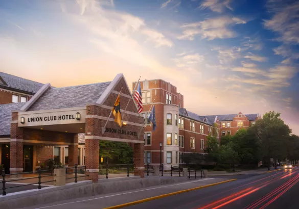
Parking on-campus can be often a challenge. Whether you stay at the Union Club Hotel, or another hotel, parking in the Grant Street Parking Garage will be the best option for the day.
Sponsorships can be tailored to meet your branding and marketing objectives. Become a sponsor and brand your company at the Midwest Breakfast Forum.
Contact Lin Tso, [email protected] to learn about available sponsorship opportunities.
Join us for the Midwest Chapter Breakfast Forum—
The Growing Semiconductor Ecosystem and U.S. Innovation in the Midwest
Join us to hear from industry leaders on their pivotal role in America’s semiconductor innovation. Listen in on discussions about how Indiana and our Midwest partners are bolstering the semiconductor industry, and how they are leveraging the exceptional talent pipeline to drive forward key innovations that will impact global markets.
SEMI Midwest Breakfast Forum is an excellent opportunity to LEARN, NETWORK, and SHARE your business solutions and ideas—Register Today!
This new regional chapter was formed to serve SEMI Members in the Midwest region. Its goal is to support member companies to grow and prosper collectively. Future chapter forums will identify, discuss, and find solutions to current topics impacting our industry.
SEMI Breakfast Forum Organized by SEMI Midwest Chapter
In-Person
Eastern Time
Hosted and Breakfast Forum Sponsored by Purdue University
The Growing Semiconductor Ecosystem and U.S. Innovation in the Midwest
In-Person | October 29, 2024
Purdue University
8:00–12:00pm ET
8:00 am - 12:00 pm
Off
Add to Calendar2024-10-29 08:00:002024-10-29 12:00:00Midwest Chapter Breakfast Forum—The Growing Semiconductor Ecosystem and U.S. Innovation in the MidwestSEMI Breakfast Forum Organized by SEMI Midwest ChapterIn-PersonEastern TimeHosted and Breakfast Forum Sponsored by Purdue UniversityIn-Person—Eastern Time Purdue Memorial Union, North Ballroom 101 North Grant Street West Lafayette, IN 47906-3574 United StatesSEMI.org[email protected]America/New_Yorkpublic
America/New_York
2
The summit will focus on the semiconductor industry's transition to renewable energy, bringing together leaders, policymakers, and experts to discuss its role in sustainable growth. Key topics include reducing carbon footprints, collaboration across the supply chain, and innovative solutions for achieving net-zero emissions. This initiative aims to strengthen the region's commitment to sustainability and position its semiconductor industry as a leader in green innovation and decarbonization.
1:30 pm - 5:30 pm
Off
Add to Calendar2024-10-10 13:30:002024-10-10 17:30:00SLS - SG Edition 2024Sustainability Transition: Collaboration - Innovation - TransitionThe summit will focus on the semiconductor industry's transition to renewable energy, bringing together leaders, policymakers, and experts to discuss its role in sustainable growth. Key topics include reducing carbon footprints, collaboration across the supply chain, and innovative solutions for achieving net-zero emissions. This initiative aims to strengthen the region's commitment to sustainability and position its semiconductor industry as a leader in green innovation and decarbonization.Meeting Room 300 - 301, Suntec Singapore Convention & Exhibition Centre 1 Raffles Boulevard Singapore 039593 SingaporeSEMI.org[email protected]Asia/Singaporepublic
Asia/Singapore
Register Now
Fueling Innovation: How California Is Still Leading the Charge in Next-Gen Semiconductor Development
REGISTRATION
EARLY BIRD PRICING—Before August 7, 2025
SEMI Members: $75 (Use your corporate email address during log in to be recognized as a SEMI Member)
Non-Members: $100
REGULAR PRICING
SEMI Members: $100
Non-Members: $125
For any questions about the event, please contact:
Sponsoring the SEMI Silicon Valley Breakfast Forum offers unique opportunities to elevate your brand, connect with industry leaders, and influence the future of semiconductor innovation.
Contact Tim Janes, [email protected] to learn about available sponsorship opportunities.
Fueling Innovation: How California Is Still Leading the Charge in Next-Gen Semiconductor Development
California has long been the heartbeat of tech innovation—where visionary R&D, strategic investment, and collaborative public-private partnerships are accelerating the future of next-generation chip technologies.
Join fellow industry leaders, engineers, researchers, and investors for a high-impact event that explores how California continues to drive global leadership in semiconductor design, fabrication, and supply chain resilience. From advanced node development to heterogeneous integration and AI-driven architectures, this event will highlight the innovations, infrastructure, and initiatives pushing the boundaries of what’s possible.
Why Attend?
Discover how California’s innovation economy and policy landscape are driving chip leadership and national security
Engage with experts across design, fabrication, packaging, and systems integration
Hear from thought leaders shaping the future of semiconductor innovation
Explore cutting-edge advances in design, materials, and manufacturing—from quantum to AI
Connect with key decision-makers across one of the industry’s most dynamic ecosystems
Whether you're scaling a startup, investing in new tech, managing supply chains, or driving state or federal policy, this is your front-row seat to the ideas, infrastructure, and innovators redefining the future of semiconductors in California—and beyond.
Don't miss this opportunity to see how California is not just keeping up—but leading the charge.
SEMI Silicon Valley Breakfast Forum—your chance to connect with top industry leaders, spark game-changing conversations, and build the relationships that drive innovation.
In-Person—Pacific Time SEMI HQ 673 S. Milpitas Blvd. Milpitas, CA95035 United States
Pacific Time | Thursday, August 21, 2025 | In-Person
8:00 am
-
8:30 am
Networking Breakfast & Check-In
8:30 am
-
8:40 am
Ajit Manocha
CEO
SEMI
Welcome Remarks
8:40 am
-
8:45 am
Na Yang
Vice President, Business Management
SCREEN & SEMI Silicon Valley Chapter Committee Member
8:00 am - 11:50 am
Off
Add to Calendar2025-08-21 08:00:002025-08-21 11:50:00Fueling Innovation: How California Is Still Leading the Charge in Next-Gen Semiconductor DevelopmentSEMI Silicon Valley Breakfast Forum In-Person—Pacific Time SEMI HQ 673 S. Milpitas Blvd. Milpitas, CA 95035 United StatesSEMI.org[email protected]America/Los_Angelespublic
America/Los_Angeles
2
Convention Hall 3, 3F, Suwon Convention Center South Korea
9:00 am
-
9:30 am
Dae-Woo Kim
Samsung Electronics
The Journey of Semiconductor Industry and the Innovation of Advanced Packaging
Competition in the semiconductor industry is becoming fiercer and advanced package technology has become important for achieving low-power and high performance computing. As the Moore’s law reach the limitation, Si fabrication process need extremely high cost solutions such as multiple patterning and EUV (Extreme Ultra-Violet) lithography. In spite of high cost Si fabrication process, chip size is increased over the reticle size limit by adding more and more functional blocks for high performance computing. In particular, with the continuous demand for higher performance and capacity in memory products, the amount of data created, processed, stored and transferred is increasing tremendously. In order to overcome these challenges, advanced package based on RDL (Re-Distribution Layer), flip chip bonding, and TSV (Through Silicon Via) have been actively used for heterogeneous integration in electronic packages since the past decade. The heterogeneous integration and chiplet has been attracting a lot of attention since it enables higher bandwidth with low power consumption at reduced cost. 2.5D Si interposer architecture has been widely used for horizontal interconnection between logic to logic and logic to high bandwidth memory integration. 3D stacking architecture is for vertical interconnections enabling small form factor, increasing signal speed, reducing power consumption and power dissipation. In this talk, recent advanced package technology and key roadmap in Samsung Electronics will be shared for mobile and AI/HPC product.
Co-Process and Co-Development to Address Challenges in Co-Packaged Optics (CPO)
Co-Packaged Optics is the combination of photonic integrated circuits and electronic circuits at a system packaging level. The essential need is to get light in and out of the system, usually from optical fibers, with the least losses and ease of manufacturing. Photonic integrated circuits (PICs) are fabricated in CMOS semiconductor fabrication facilities, which allows manufacturers to take advantage of the large installed base of tools and processes. However, electronic packaging is currently not equipped to handle the challenges associated with packaging advanced photonic devices. In this presentation we explore some of these challenges for optical coupling such as sub-micron alignment tolerances, sensitivity to temperature variations, optical losses, and a lack of standards. The end objective is to have optical coupling look like electronic coupling. At NYCREATES/AIM Photonics, we have learned that the best results are obtained when the PIC manufacturing and packaging processes are co-designed to better achieve low-loss coupling, particularly between photonic integrated circuits and other elements in the system. A complete “end-to-end” approach includes customizing the PIC process, wafer manufacturing including interposers and heterogeneous integration, electronic photonic design automation, and electronic-photonic test, assembly and packaging capabilities. A complete approach will lead to reliable and affordable solutions that will ensure the manufacturing-readiness of this critical technology for decades to come.
Advanced Packaging Technology for HBM and 2.5D SiP
Rapid growth of generative AI at this moment has never been experienced for a few decades and it makes surprising impact to human experience and semiconductor industry as well. High bandwidth memory (HBM) which started from memory solution for high-end graphic applications has being emerged as a key driver accelerating the growth of AI industry due to remarkable advantages on the smaller latency between memory and GPU.
SK hynix has been the pioneer of HBM in all of history and firstly wrote a new record by the world-first development of HBM package in 2013. More remarkable footprint in the HBM history was the world-first adoption of the mass reflow bonding and molded underfill (MR-MUF) technology to the HBM 4Hi and 8Hi in 201, which nobody has never tried due to its notorious difficulties of process and material technologies. In this effort, SK hynix is providing a state-of-the-art of HBM products with highest memory bandwidth and memory capacity, highest power efficiency, and superior thermal dissipation ability and its package technology is a core competency leading the memory renaissance in the post-pandemic era.
In align with HBM technology innovation, there are continuous changes in 2.5D system-in-package (SiP) in order to improve the memory bandwidth and accommodate higher memory capacity. There has been many different types of proxy package structure to assure the HBM quality and reliability but it is obviously not certain whether HBM package can guarantee all the possible quality and reliability risks due to many possible changes of HBM and SiP packages in the future. In this paper, we would like to introduce several ways to evaluate the thermal and electrical characteristics of HBM and its package reliability.
The AI era has arrived and to enable and perpetuate it, the semiconductor advanced packaging (AP) industry needs to innovate in a torrid pace to keep in tandem the exponential growth of the Gen AI computing power.
Rising to the challenge, ASMPT has been leveraging its first mover market position in advanced packaging to continue innovating its end-to-end solutions to scale with the latest packaging architecture with the most demanding chiplet interconnects and heterogeneous integration formats.
Going forward, the AP industry shall undergo a “Power of N” transformation where interconnect pitch shall shrink rapidly along with thinner and bigger package formats, demanding new technologies in materials, process and equipment signaling a need for a complete and robust ecosystem to evolve for Gen AI to continue scaling.
As artificial intelligence (AI) continues to advance, the demand for high-performance computing has never been greater. Advanced packaging technologies play a pivotal role in meeting these demands by enhancing the performance, power efficiency, and integration density. This presentation explores the impact of various advanced packaging solutions, including 2.5D with Si interposers, 2.3D with RDL interposers, and 3D packaging technologies, on the development and optimization of AI systems.
We will delve into the specifics of 2.5D packaging, where Si interposers enable the integration of heterogeneous dies side by side, allowing for high-bandwidth communication and reduced latency. The presentation will also cover 2.3D packaging with RDL interposers, which offer a cost-effective alternative by utilizing advanced RDL processes to achieve similar benefits as 2.5D, but with potentially lower manufacturing complexity and cost.
Furthermore, we will examine 3D advanced packaging technology, which stacks dies vertically to further enhance integration density and performance. This approach not only maximizes space efficiency but also minimizes interconnect lengths, leading to significant improvements in speed and power consumption which are critical factors for AI applications.
Through a comprehensive analysis, this presentation will highlight how these advanced packaging technologies contribute to the acceleration of AI innovation, enabling more powerful, efficient, and compact AI packaging solutions.
Big data, artificial intelligence (AI), and high-performance computing (HPC) underscore the critical importance of advanced packaging technologies. Over the past decade, significant progress in 2.5D and 3D heterogeneous integration has led to notable improvements in I/O capacity, performance, cost efficiency, power consumption, and signal speeds for large-scale data processing.
In particular, 2.5D semiconductor packaging technologies such as EMIB and CoWoS are crucial for increasing I/O connections while reducing the interconnect length between logic and memory components, thereby enhancing performance and reducing latency.
However, FCBGA substrates used in AI/HPC packaging face considerable technical challenges. These substrates often need to be larger than 100mm x 100mm and consist of more than 20 layers. Furthermore, incorporating advanced technologies like silicon capacitor embedding and bridge integration into large-body FCBGA substrates presents additional hurdles as the industry moves towards next-generation packaging solutions.
This presentation thoroughly explores the latest technology trends in FCBGA substrates.
As the demand for higher performance, greater miniaturization, and improved thermal management continues to grow in the electronics industry, advanced packaging technologies are becoming increasingly critical. Glass substrates are emerging as a key material in this domain, offering unique advantages over conventional organic and silicon-based substrates. This talk explores the present and future potential of glass substrates in advanced packaging, focusing on their electrical, thermal, and mechanical properties that make them suitable for next-generation semiconductor devices.
It will also highlight recent innovations in glass substrate manufacturing, such as through-glass vias (TGVs) and surface modification techniques, which enhance the performance and reliability of electronic components.
Semiconductor Integration & Packaging: Powering AI and HPC The Advanced Packaging Summit is a conference dedicated to exploring the latest advancements in packaging technology for high-performance computing (HPC) and AI. The summit brings together leading experts, researchers, and industry professionals to share their insights and experiences on advanced packaging solutions that enable powering AI and HPC systems. Topics covered at the summit include 2.5D packaging, Chiplet packaging, CPO, FCBGA substrate technology and more. Attendees will gain valuable insights and have the opportunity to network with experts in the industry.
Advanced Packaging Summit 2024
9:00 am - 5:30 pm
Off
Add to Calendar2024-09-11 09:00:002024-09-11 17:30:00Advanced Packaging Summit 2024Semiconductor Integration & Packaging: Powering AI and HPCThe Advanced Packaging Summit is a conference dedicated to exploring the latest advancements in packaging technology for high-performance computing (HPC) and AI. The summit brings together leading experts, researchers, and industry professionals to share their insights and experiences on advanced packaging solutions that enable powering AI and HPC systems. Topics covered at the summit include 2.5D packaging, Chiplet packaging, CPO, FCBGA substrate technology and more. Attendees will gain valuable insights and have the opportunity to network with experts in the industry. Convention Hall 3, 3F, Suwon Convention Center South KoreaSEMI.org[email protected]America/Los_AngelespublicDiscover APS 2025