Suzhou Shi
Jiangsu Sheng
China
Suzhou Shi
Jiangsu Sheng
China
Event Host
“How Will Agentic AI Change Chip Design and Verification?” features EDA and emerging agentic AI company executives and entrepreneurs discussing changes within chip design and verification as agentic AI tools become more mainstream. Panelists will distill the excitement surrounding the innovation in chip design and verification, collaboration between traditional EDA and agentic AI startups and broader implications for technological advancements.
Cadence Design Systems
2655 Seely Avenue
Building 10
San Jose, CA 95134
United States
Registration and Networking with Dinner and Beverages
Welcome and Speaker Introductions
Moderated panel discussion and Q&A
Join ESDA for our Executive Outlook event, "How Will Agentic AI Change Chip Design and Verification?"
5:30 pm - 8:30 pm Off Add to Calendar Disabled America/Los_AngelesRegistration
- Early-Bird Registration Deadline: Wed, May 7, 5PM (KST)
- Group Registration Deadline: Fri, May 2, 5PM (KST)
Registration Fee
- Early Bird
- SEMI Member: KRW 308,000
- Non Member: KRW 363,000
- On site
- SEMI Member : KRW 385,000
- Non Member: KRW 385,000
- Group
- SEMI Member : KRW 275,000
- Non Member: KRW 330,000
*Group registration fee applies to groups of five or more from the same company.
*For group registration inquiries, please contact SEMI Korea Program Team([email protected]).
OVERVIEW
- Date: May 14(Wed), 2025
- Time: 9:00-16:20
- Venue: Convention Hall 2, 3F, Suwon Convention Center
NOTICE
- The agenda is subject to change at the discretion of the speakers.
- Registration fee includes a boxed lunch provided at the venue.
- Simultaneous interpretation will be provided.
- Presentation files agreed by speakers will be provided to attendees after the event through SEMI registration website.
SPONSORS
![]() | ![]() | ![]() | ![]() |
![]() | ![]() | ![]() | ![]() |
![]() | ![]() |
![]()
CONTACT
- SEMI Korea Program Team ([email protected])
Convention Hall 2, 3F, Suwon Convention Center
South Korea
Welcome Reception
Materials Innovation for 3D DRAM/ CFET
As the era of lateral shrink is coming to a cliff, the need for looking at the remaining axis is uprising - the Z-axis. For DRAM, the introduction of vertical channel is very near, and even the introduction of a full 3D-DRAM is not far away. Fortunately, we have experience of VNAND, which could tell us many things about the difficulties following the 3D stacking structures. Starting from the change in the material we've gone through regarding the conversion of planar to vertical NAND, prospection of the material innovation for 3D-DRAM will be shared. The introduction of materials for the construction of deep holes and lengthy lines will be addressed. Also, needs for innovative sacrificial and auxiliary materials will be presented.
Memory technologies : Status and Scaling
As DRAM scaling approaches fundamental limits, advanced architectures such as 3D DRAM and 4F² DRAM have emerged as promising solutions. The industry initially anticipated the adoption of these technologies around the 1d to 0a nm nodes; however, they remain in development, with mass production likely postponed until the 0b node. For instance, current 3D DRAM samples feature 8–12 layers, while the target is approximately 90 layers. Recent advancements include 3D DRAM with vertical bit-line architecture, demonstrating improved on-current performance and gate control through 5-layered cell stacks utilizing Si/SiGe sacrificial layers and hybrid bonding. Meanwhile, novel 4F² DRAM transistor structures exhibit enhanced operational margins and mitigate floating body effects through dual-gate designs. Additionally, a 3D stackable DRAM architecture with horizontally stacked transistors has been proposed to address challenges such as gate-induced drain leakage (GIDL) and row hammer effects, supported by both experimental and simulation results. Collectively, these innovations underscore the potential of 3D and 4F² DRAM as next-generation solutions to overcome scaling bottlenecks and meet the growing demand for high-density, low-power memory.
Materials and Process Technology Perspectives for CFET Device
The development of semiconductor technology can be continuously achieved through the collaboration of materials, processes, devices, and systems, and 3D devices and 3D integration process technologies will be essential in the future. From this perspective, the structural change of semiconductor transistors is expected to evolve from the current Gate-All-Around FET (GAAFET) to a new Complementary FET (CFET) device. This structural change of semiconductor devices requires new materials and process technologies. Various technologies are required, such as Monolithic or Sequential 3D integration, Si/Si or Si/Non-Si substrates, new low-resistivity metals, CMP, Bonding, TSV, and Back-Side Power Network Delivery (BSPDN). In this presentation, we will examine the technological trends from the materials and process perspectives for the development of CFET device technology.
Si, Ge, B Hydrides for Next Generation Semiconductor Devices – Challenges and Perspectives
For the past six decades, hazardous gas hydrides like GeH4, Si2H6, and B2H6 have been essential to the semiconductor industry. Their high reactivity, strong reducing power, and ability to grow high-quality, carbon-free layers have made them vital for applications ranging from Si and SiGe epitaxy to tungsten metallization. In recent years, new applications and integration schemes have emerged, demanding higher-performance hydride sources for low-temperature Chemical Vapor Deposition (CVD) and epitaxy. This increased global demand drives production investments, despite the challenges of handling, facilitating, and logistics constraints such as limited shelf-life, pyrophoricity, and toxicity. In this talk, we will provide an overview of the current gaseous hydrides landscape and its challenges. We will discuss how the gas industry can ensure the semiconductor industry's continued safe access to these critical materials through enhanced stewardship, optimized supply chains, packaging, and manufacturing techniques. Furthermore, we will provide insights into technology trends towards new-generation, extra-low-temperature epitaxy and high dopant sources, and their potential use in future transistor architectures.
Networking Break
Panel Discussion
Lunch
Materials Engineering Innovations to Address HBM Challenges for AI Applications
Emergence of artificial intelligence (AI) is predicted to drive global chip sales to ~$1 trillion revenue by 2030. This surge of AI-targeted chip demand is driving ever-increasing requirement in compute speed to >109 petaFLOPS. High-bandwidth memory (HBM) architecture is well-suited to fulfill this requirement, currently offering >1TB/s bandwidth. To continue improving HBM performance, materials engineering innovations are required in critical packaging building blocks, such as TSV and Hybrid Bonding. Solutions from equipment manufacturer standpoint were presented, in relation to TSV gapfill, low-temperature (<300˚C) hybrid bonding enablement, and bond strength consideration for higher I/O count in the future. Timely solutions to the dynamic HBM integration challenges should be seen holistically and to this end, active partnerships and collaboration across the ecosystem are encouraged.
Semiconductor Materials Supply Chain and Market Development Trends
The semiconductor industry continues to advance, propelled by growing demand for AI-driven computing and storage technologies and diverse digital applications. However, this growth is tempered by rising economic uncertainty and escalating trade tensions, particularly due to recent U.S. tariff policies, which threaten to disrupt global supply chains. The semiconductor materials sector faces multifaceted challenges, including increasing rapid technological innovation, geopolitical volatility, large-scale capacity expansions and climate change actions. While the market remains relatively stagnant in 2024 compared to 2023, a rebound is anticipated in 2025–2026, driven by long-term demand for advanced computing and storage solutions. A shifting supplier landscape is emerging, marked by the rise of regional players—notably in China—and consolidation among multinational corporations pursuing economies of scale through mergers and acquisitions. Geopolitical pressures are driving localization and dual sourcing, which raise costs, reduce efficiency, and complicate supply chains. This talk highlights the need for a delicate balance between innovation-driven growth and the escalating operational challenges in the semiconductor materials industry.
Networking Break
Technological Trends and Necessity of Material Contamination & Filtration for Wafer Defectivity Control in HBM Manufacturing
As the commercialization of artificial intelligence (AI) and the advancement of technologies such as high-performance computing (HPC) and deep learning (DL) progress, the need to process large amounts of data quickly has emerged. Traditional DDR and GDDR memory have limited bandwidth, so HBM, which offers higher performance, has been commercialized, driving the development of new technologies.
Compared to traditional memory chips, HBM has increased chip size and higher defectivity vulnerability due to chip stacking processes. This has led to new technical approaches for wafer defectivity control across the entire material ecosystem.
This presentation reviews the latest trends in filtration/purification technologies aimed at minimizing the impact of particles and impurities in this material ecosystem. By examining current HVM devices and next-generation HBM-related technologies, we aim to contribute to wafer defect control.
Advancing ALD Tool Qualification Using Ultra-High-Aspect-Ratio Test Structures
As semiconductor manufacturers continue the vertical scaling of 3D memory devices, advanced metrology and process control strategies are becoming increasingly essential for maintaining yield and reliability. The rising aspect ratios (AR > 100) of device features present significant challenges for conformal thin-film deposition via atomic layer deposition (ALD). Ultra-thin dielectric films and multilayer stacks—widely used in 3D memory channel holes—are particularly sensitive to process variations. Even minor deviations in ALD process conditions can result in non-uniform film coverage, defect formation, or electrical performance issues, all of which are difficult to detect and monitor within high-aspect-ratio structures.
To address these challenges, Chipmetrics has developed a novel method based on lateral ultra-high-aspect-ratio test structures (PillarHall®) for ALD process development, monitoring, and tool qualification. In the PillarHall® test wafers, the aspect ratio exceeds 1000, enabling practical and non-destructive measurement of film conformality. The method offers a sensitive and scalable solution for improving ALD process qualification, benchmarking tool performance, and enhancing production stability.
This presentation will highlight recent advancements in PillarHall® technology, with a focus on its application in ALD tool qualification and ALD process window control.
The Role and the Challenge of the Process Material for the Future of Semiconductor
There have been lots of technical advances in the fileld of semiconductor industry for the last dacades ever since DRAM and NAND were invented and commercialized. Meanwhile, form factor was changed from 8F2 to 6F2 in DRAM, and the concept of 3D stacking was adopted in NAND flash memory. Furthermore, EUV tool has been adopted and are being successfully used to make the fine pattern in logic and DRAM as well. And also, it has been very long since ALD was taken as a new advanced depostion technology to meet the need for excellent conformality. But all these new process technologies couldn’t have been possible without the advances in process materials such as advanced photo resist, precursors, functional chemicals and CMP slurries. Recently, those process materials are beginning to open the new possibilities for the innovation of process integations, resulting in cost reduction and giving an extra performance to the process tools. In this talk, the role, the current issues and future challenges will be discussed focusing on the process materials in semiconductor industry.
Starting from photo resist, thin and etch resistant resist has been cosistantly required to suppress the pattern collapse and wiggling during the patterning process. Since the EUV was adopted in DRAM and Logic, high sensitivity EUV resist is now being intensively explored to obtain low DtS as well as good CD uniformity to make the best use of the enomoursly high-priced EUV tool in a cost effective way. For the sake of that, even metal-containing resist is also being tried for high quality patterning. Additionally, thick KrF resist is also required at 3D NAND flash memory with the increase of ON stack and especially for the new platform to be. And for the future, the new concept of PR based on small sized polymer will be worth trying and dry type developer would be also necessary to keep the pattern stable without collapse or wiggling.
With regard to the wet chemicals and CMP slurries, advanced functional chemicals are getting more and more important rather than convetnional cleaning chemicals that are used after etch and CMP process. W or Mo recess chemical in 3D NAND would be that very case. Those chemicals should assure the good uniformity in terms of recess amount in the vertical direction. Most of all etch and CMP prcesses need post cleaning steps to clean the residue, but during that, some unwanted part of the surroundings is apt unavoidably to be removed deteriorating the device proformance in the end. Therefore, special clean chemical will be also needed to minimize the unwanted film loss as well as residue removal. When it comes to the slurry, the shape of the abbrasive particles consistently has been changing from sharp and pointed to the rounded one by adopting colloidal synthesis to suppress the scratch during CMP. The size of the abrasive particle tends to get smaller but slurry is required to make up the decreased removal rate by properly regulating components within slurry. With the change of material to be polished such as Mo or Carbon, new slurry for those new materials will be a new drive for CMP related materials.
Precursor and some functional gases have been contributing to the quality improvement or deposition modication of functional materials such as high-k materials in DRAM. As always, there should be more technical areas, in which precursor and gas will be able to play an important role in ASD(Areal Selective Deposition) or ALE(Atomic Layer Etching) process.
Since process materials needs to be considered from the operation of FAB line unlike the process tools, it must be managed well from the aspect of consistent quality control and risk management of supply chain and safety. In the past, process material used to play a simple and supporting role in the process and tools as well. But now, it is becoming a time for the process materials to play a more active role in cost reduction and risk management as well as providing technology for semiconductor industry. Especially, new process materials are also required to meet the needs for low carbon emission during the process and safety issues from the using PFAS containg materials that are hazardous to human body. Way of doing work needs to be also changed in a way that R&D activities have to be shifted to the earlier engagement. And plus, the collaboration between device maker and process material supplier shoud be much closer and earlier than before so that the developed materials can be successfully adopted at a targeted process and a tool for it. As the material supply chain has been becoming very unstable since corona pandemic and US-China trade conflict, it needs to be managed with a good predictability and balance as well in order for consistent and stable supply in case of unexpected issues at a supply chain.
Adjourn
Empowering the AI Era: Advancements in Next-Generation Memory and Materials
The arrival of the AI era demands transformative advancements in memory technology and semiconductor materials. This year, SMC (Strategic Materials Conference) Korea will focus on the innovative materials and manufacturing technologies driving the development of next-generation memory technologies in response to the AI-driven technological revolution. The first session will explore material innovations emerging from the evolution of next-generation memory semiconductor technologies, such as 3D DRAM and CFET. The second session will offer in-depth discussions on the future of semiconductor materials related to cutting-edge memory manufacturing, such as HBM, from diverse perspectives, including global equipment and material suppliers, integrated device manufacturers (IDMs), and semiconductor research institutions. Additionally, a panel discussion featuring all speakers will provide an opportunity for deeper exchanges of valuable insights. We encourage your active participation in this conference to engage in meaningful discussions and gain a more comprehensive understanding of the topics.
9:00 am - 4:20 pm Off Add to Calendar 2025-05-14 09:00:00 2025-05-14 16:20:00 SMC (Strategic Materials Conference) Korea 2025 Empowering the AI Era: Advancements in Next-Generation Memory and Materials The arrival of the AI era demands transformative advancements in memory technology and semiconductor materials. This year, SMC (Strategic Materials Conference) Korea will focus on the innovative materials and manufacturing technologies driving the development of next-generation memory technologies in response to the AI-driven technological revolution. The first session will explore material innovations emerging from the evolution of next-generation memory semiconductor technologies, such as 3D DRAM and CFET. The second session will offer in-depth discussions on the future of semiconductor materials related to cutting-edge memory manufacturing, such as HBM, from diverse perspectives, including global equipment and material suppliers, integrated device manufacturers (IDMs), and semiconductor research institutions. Additionally, a panel discussion featuring all speakers will provide an opportunity for deeper exchanges of valuable insights. We encourage your active participation in this conference to engage in meaningful discussions and gain a more comprehensive understanding of the topics. Convention Hall 2, 3F, Suwon Convention Center South Korea SEMI.org [email protected] Asia/Seoul public Asia/SeoulRegistration
Please be sure to check / understand the followings before applying
- Due to the nature of this product, we do not accept cancellations or refunds after the application has been made. Please understand this in advance.
- When applying for this event, please register using a corporate email address.
- SEMI Member Price is avilable for those who work for a SEMI member company or a wholly owned subsidiary that is registered as a subsidiary. If you are unsure, please click HERE to inquire. Please note that if your membership status cannot be confirmed, you will be charged the general price.
- Payment is only possible by credit card. You can download your receipt from Receipt / Application History in your My Page.
Please note that places will be allocated on a first-come, first-served basis, so please apply as soon as possible.
First deadline: June 6 (Fri)
Final deadline: June 25 (Wed)
- Symposium Fee
SEMI Members : 230,000 JPY / Non-Members : 460,000JPY
Please note that you will be responsible for the cost of local accommodation, transportation and participation in the golf competition.
A shuttle bus service is scheduled to run between New Chitose Airport and the venue. - Accommodation Charge
45,600JPY ~ 48,600JPY per night (Include Breakfast) - Golf Competition Participation [option]
25,000JPY - Travel Expenses
Please bear your own travel and transportation expenses to New Chitose Airport.
SEMI Japan Event Registration
Email: [email protected]
Accommodation and Shuttle Bus
Please see below for details on accommodations and shuttle buses.
The Windsor Hotel Toya Resort & Spa
336 Shimizu, Toyako-cho, Abuta-gun, Hokkaido 049-5722
Superior Room Sea Side (40㎡) (Non-Smoking)
1 person usage: 50,460 JPY / night (per person)
2 people usage: 27,800 JPY / night (per person)Superior Room Lake Side (40㎡) (Non-smoking)
1 person usage: 53,760 JPY / night (per person)
2 people usage: 29,450 JPY / night (per person)*Breakfast, consumption tax, bathing tax, and service charge are included.
[Outbound] July 10 (Thu) New Chitose Airport → Windsor Hotel Toya Resort & Spa
- Duration: 120 minutes
- Fare: Free (application is required)
- Meeting/departure time: 8:30-10:00 Please arrive at New Chitose Airport on your flight. We offer multiple flights to suit your flight arrival time.
[For reference] Flight Schedule
New Chitose Airport / ANA / JAL
[Return] July 12 (Sat) Windsor Hotel Toya Resort & Spa → New Chitose Airport
<Those who do not participate in the ISS Golf Competition>
- Duration: 120 minutes
- Fare: Free (application is required)
- Meeting/departure time: 9:00 / 10:00 / 11:00
<Participants in the ISS Golf Competition>
Buses from the hotel to the golf course and from the golf course to the airport are available separately.
Details such as meeting time will be announced at a later date.
JTB Global Marketing & Travel
SEMI ISS Hokkaido 2025 Desk
*Inquiries can be received only by e-mail.
E-mail: [email protected]
Office Hours: 10:00-16:30 (Mon-Fri except Saturdays, Sundays and Holidays)
Platinum Sponsor

Gold SAKURA Sponsor


Overview
We will be holding “ISS Hokkaido 2025”, a conference to discuss strategies and issues with an eye on the future of the industry.
As digital technology supports global prosperity, we will provide opportunities for exchanging opinions and networking on important issues such as sustainability, energy issues, and the latest technology, in order for Japan to demonstrate leadership as an important base for semiconductor manufacturing.
(includes Government Officials, Top Executives of Semiconductor Device, Equipment, Material, and Component Companies)
Symposium Agenda
[Simultaneous interpretation]
*Titles omitted
*Please note that the program is subject to change.
Thursday, July 10, 2025
Conference Check-In, Lunch


Session 1 Opening
Jim Hamajima
President
SEMI Japan
Opening Remarks

Ajit Manocha
President & CEO
SEMI
SEMI Industry Update

Satoshi Nohara
Director-General, Commerce and Information Policy Bureau
Ministry of Economy, Trade and Industry
Coffee Break


Session 2 Global Leaders of Semiconductor Industry


Thomas Piliszczuk
Worldwide Strategic Partnerships & Strategy
Executive Vice President
imec
The Versatile Future of Semiconductor Systems
The last few decades have seen a remarkable increase in technology applications, culminating in the AI revolution. Thanks to Moore's Law, technological advances are enabling more powerful applications, especially for the rapidly growing computing needs of AI. Maintaining Moore's Law and adopting new architectural approaches are key to efficiently handling the exponential increase in computing power required, leading to a demand for more flexible chip architectures and platforms. Significant advances in the semiconductor industry have been driven by state-of-the-art infrastructure, a global ecosystem and skilled talent. Legislative initiatives such as the Chips Acts provide an ideal framework for increasing collaboration and impact in the semiconductor sector. These elements are essential for the advancement of various technology platforms, laying the foundation for advanced computing systems in future applications.

Masataka Osaki
Japan Country Manager, VP Worldwide Field Operations
NVIDIA
NVIDIA AI Revolution
How we build Sovereign AI is the another hot topic in Japan as well. By introducing early success stories in Japan will bring another light to our path for the future.

Tomoharu Watanabe
Executive Vice President and Executive Officer
Kioxia
Kioxia’s Growth Strategy and Manufacturing
Coffee Break

Session 3 Economic & Market Trends

Josephine Lau
Senior Market & Technology Analyst
Yole Group
Future of the Semiconductor Market Through AI, Memory, and Supply Chain Resiliency
This presentation explores how AI is not only a catalyst but a long-term compounder of semiconductor demand - driving exponential growth in compute-intensive applications and fueling the need for advanced memory solutions. At the heart of this AI - driven surge lies memory - specifically High Bandwidth Memory (HBM) and 3D DRAM—which are emerging as critical enablers and strategic differentiators in the race for performance, efficiency, and scale.
We will examine the market size and trajectory of memory technologies, unpack the technology roadmap for HBM and 3D DRAM, and highlight how these innovations are becoming the new battlegrounds for leadership in the semiconductor value chain. Finally, the session will address the imperative of supply chain resiliency, showcasing how cross-border memory production strategies and ecosystem collaboration are creating durable competitive moats in an increasingly fragmented global landscape.

Clark Tseng
Sr. Director,
Market Intelligence Team
SEMI Taiwan
Navigating Semiconductor Growth in Uncertainty: Opportunities and Challenges for Japan through the Lens of Fab Investment
A key focus of this presentation will be an in-depth analysis of SEMI's World Fab Forecast reports, providing insights into the latest capital equipment forecasts by region and key segments. We will examine the fab investment outlook, capacity growth projections through 2028, and the regional distribution of fab projects, with particular attention to leading-edge logic technologies and mainstream nodes. Furthermore, we will discuss the impact of government incentives on global fab investments, a crucial factor in the evolving semiconductor ecosystem. Finally, we will share SEMI’s latest forecasts on wafer fab materials, providing a comprehensive view of the industry's material requirements.
In this presentation, we aim to provide valuable insights to assist industry stakeholders in navigating the opportunities and challenges of the semiconductor industry's growth wave. We will explore how Japan can leverage its strengths in technology to capitalize on the burgeoning demand for advanced semiconductors and contribute to the industry's continued advancement.
Welcome Reception & Dinner


Friday, July 11, 2025
Session 4 Japan's International Competitiveness

Daishiro Yamagiwa
Member, House of Representatives
Liberal Democratic Party

Masaru Tsuchiya
Partner, Japan Office
McKinsey & Company
Paving the Way for a Semiconductor Renaissance in Japan

Lily Feng
President
SEMI China
Exploring Promising Opportunities of China Semiconductor Industry
Coffee Break


Session 5 Geopolitics and Economic Security

Takahide Kiuchi
Executive Economist
Nomura Research Institute
Trump’s Tariffs and the Japanese Economy

Shingo Yamagami
Special Advisor
TMI Associates
Strategic Challenges Facing Japan

Lin Chen-wei
Senior Advisor
Pacific Solutions, LCC
From Chip War to Global Security: Taiwan's Strategic Value
Lunch


Session 6 Round Table Discussion
①Geopolitics
②International Competitiveness
③Supply chain Resilience
Coffee Break


Session 7 The Insights from Round Table Discussion
Session 8 Session 8 Grand Finale

Atsuyoshi Koike
CEO
Rapidus
Jim Hamajima
President
SEMI Japan
Closing Remarks
Dinner Party
ISS Networking Golf

Golf course
New Chitose Country Club Hamanasu Course
(1392 Kyowa, Chitose City, 066-0005)
Date
Saturday, July 12
Schedule
05:00 Departure from the hotel
07:00 Arrive at the golf course
07:35 Start of Group 1
13:30 Last group ends
14:00 Competition Party
14:45 Competition party ends
15:00 Depart from golf course
15:30 Arrive at the airport
*Please book a return flight departing from New Chitose Airport after 16:30.
The Windsor Hotel TOYAResort & Spa
Shimizu, Toyako-cho, Abuta-gun
Hokkaido
049-5722
Japan
ISS (Industry Strategy Symposium)
Hokkaido 2025
[For Those Who Applied]
For detailed information on the day of the event, please click here.
To issue a receipt or check or correct your registered information, please visit My Page.
Related blogs
2025-05-26
Europe’s Semiconductor Strategy: Navigating Geopolitics, Building Resilience
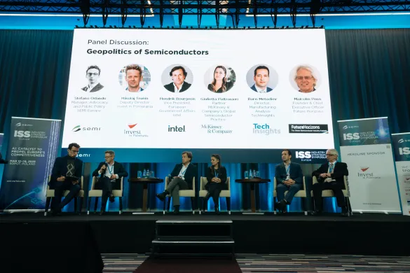
As geopolitical dynamics continue to influence global industries, the semiconductor sector finds itself at a pivotal crossroad. During the SEMI Industry Strategy Symposium (ISS Europe) held in Sopot, Poland, a high-level panel on the Geopolitics of Semiconductors brought together leaders from across the ecosystem to explore Europe’s role in an increasingly fragmented world shaped by strategic dependencies and evolving alliances.
Message

From July 10 to 12, SEMI hosts the symposium “ISS (International Strategy Symposium) Hokkaido 2025” in the summery setting of Toya, Hokkaido.
As the name “International Strategy” suggests, this symposium was established as a forum to discuss global strategic issues in the semiconductor industry from a management perspective. It is being held in three regions—the United States, Europe, and Japan—including Japan for the first time.
For this event in Japan, we have selected the Windsor Hotel, which previously hosted the Toyako Summit, as the venue. We believe this location is ideal for closed-door
discussions on global management strategies that are not typically possible on a regular basis.
At this venue, we will invite leading figures in the semiconductor industry to discuss sustainability, energy issues, and the latest technologies. Participants will include Mr. Masataka Oosaki, Representative Director of NVIDIA Japan; Mr. Yuji Watanabe of Kioxia; Mr. Thomas Piliszczuk of imec; Mr. Daishiro Yamagiwa, Chairman of the Liberal Democratic Party's Semiconductor Strategy Promotion Parliamentary League; Mr. Shinji Yamagami, an expert in diplomacy; and Mr. Seong-Woo Lim, who has played a key role in Taiwan's semiconductor strategy, among other top industry leaders.
We will also provide opportunities for attendees to participate in discussions. The discussion themes, aligned with the symposium's objectives, are “geopolitical risks,” “supply chain resilience,” and “enhancing international competitiveness.”
“ISS Hokkaido” is an excellent opportunity to discuss strategic plans for the future of the semiconductor industry. We hope that you will take this opportunity to deepen your understanding of the future of the semiconductor industry alongside executives at the forefront of the industry and contribute to the further development of the semiconductor industry in our country.
The first deadline for applications is June 6. We sincerely look forward to your participation.
Jim Hamajima
President
SEMI Japan

SEMI’s Industry Strategy Symposiums bring together executives from across the global semiconductor design and manufacturing ecosystem to examine key industry trends, forge new partnerships and relationships, and share knowledge and expertise. Generally, I have leveraged our ISS events to make calls-to-action to the assembled leaders on our programs to collaborate on key industry challenges and advance the industry. I encourage you to join us at our first ISS in Japan to be a part of these crucial discussions to secure our industry’s future growth.
Ajit Manocha
President & CEO
SEMI
Why ISS?
ISS (Industry Strategy Symposium) is, as its name suggests, a forum for in-depth discussion of strategies for industry.
With the advent of an era in which digital technology will drive global prosperity, semiconductors, which form the foundation of this technology, are indispensable to all industries. Japan, as a key hub for semiconductor manufacturing, aims to maintain its position as a global leader in cutting-edge technology.
ISS provides a platform where executive leaders can share insights from global visionaries and experts on critical issues such as sustainability, the future of miniaturization technology, evaluating new technologies, AI-driven efficiency, geopolitical tensions, and market changes driven by DX and AI implementation, and engage in direct dialogue.
Why Hokkaido?
Japan is at the forefront of this transformation, with Hokkaido emerging as a prime location for semiconductor manufacturing due to its well-developed infrastructure, favorable climate, and policy incentives. The formation of a next-generation semiconductor ecosystem is underway. Hokkaido is also a renowned resort destination, attracting visitors from around the globe with its winter landscapes of pristine powder snow and summer scenes of vibrant flower fields and majestic natural beauty. Discussions held in the private, natural surroundings of this region are sure to yield innovative and exceptional outcomes that could never be achieved in a conventional meeting room.
Invitations and Registration
REGISTRATION FOR GCSW is CLOSED.
All sessions are free of charge to Semiconductor Climate Consortium (SCC) and Energy Collaborative (EC) members. Others will be admitted by invitation on a case-by-case basis. Multiple attendees (up to 3) from your company are welcome, but must be invited. Exceptions can be made to the 3 persons limit to have the RIGHT people, with direct responsibility for subjects being discussed.
Objective of GCS Workshops
A gathering of the semiconductor value chain in one place to most efficiently share solutions and tools and workshop solutions, thereby optimizing your time and resources dedicated to addressing the specific challenges we face. The GCS Workshops are co-hosted by SEMI, the Semiconductor Climate Consortium, Apple, and Google.
The Workshops are focused on revealing the right details and data that will support action on decarbonization recommendations. The Workshops will NOT focus solely on the issue and roadblocks, but rather the solutions, including (1) sharing examples of successful paths, (2) provide possible tools you need to help address the gaps, and (3) active workshopping on further solution spacing towards emission reductions. We have identified leaders with the experience and knowledge to move toward answers during each Workshop.
Bring your experience, critical thinking skills, and share with your fellow sustainability travelers.
Workshop Themes and Layout
5/15 – Opening + Facilities Abatement Tours (Tours are now full)
5/16 (AM) - Manufacturing Scope 1 Emissions – brownfield abatement retrofits, low GWP gas substitution and emission measurements reduction solutions, toolkits, roadblocks
5/16 (PM) - Manufacturing Energy Efficiency – fab/subfab interoperability, toolkits and ROI calculations
5/19 (AM) - Renewable Energy Education & Advocacy – global state-of-play, market breakouts for education and solution short listing
5/19 (PM) - Manufacturing Scope 3 Materials Decarbonization – partner paths, impacts and tools
5/20 (AM) - Data & Reporting Alignment – ROI and roadblocks + Closing (PM)
Synergies with the Semiconductor Climate Consortium
Many themes of the GCS Workshops are outcomes of the discoveries in the SCC Working Groups and previous Supplier Day presentations. The GCS Workshops will allow for greater depth of discussions and face-to-face solutioning opportunities. With the right information and the right audience, attendees will depart with tools to operationalize for action. Across the ecosystem, we want to see those benefits show up in our Scope 3 calculations.
Microsoft Offices & Sands Convention Center
Singapore
Singapore
Registration & Networking Lunch
Meet and connect with key industry stakeholders, policy leaders, and Microsoft’s sustainability leadership.
SEMI Global Climate Summit Workshops: Welcome
Energy in the APAC Region: Outlook & Strategies
Journey to Carbon Neutral - Supply Chain Focus
Reflections on Microsoft Supplier Days & Looking Forward
Overview of GCSW Workshops
Facilities Abatement Tours
(Tours are full and no longer available to new registrants.)
Workshop 1: Manufacturing Fab Scope 1 Emissions
Breakfast and Networking
Collaborative solutions for emissions challenges
Fabs Deploying new abatement tech; brownfield retrofits
Innovative ways to complete brownfield retrofits while minimizing fab disruption
New abatement tech for both greenfield & brownfield fabs
Samsung's journey to net zero & Scope 1 strategies
Workshop 1
- Retrofits: Learnings; forward-looking; benchmark projects; modular approaches
- Abatement Technology / Performance Roadmap: accelerating timelines; trends; alignment
Low GWP Gases
Workshop 2: Risk assessment & Methodology
Emissions Measurement
Workshop 3: Real-time monitoring, calibration variation, regulatory
Readouts & Lunch Break
Workshop 2: Manufacturing Energy Efficiency – fab/subfab interoperability, toolkits and ROI calculations
IDM perspective, state of the art sensor deployment & best practices for energy efficiency
Immediate Opportunities around Energy Efficiency
ASM Energy Efficiency Story
Net Zero Operations through Innovation and Collaboration
EE Workshop 1: Sensor Deployment for Equipment
From energy sensor to harmonics & power quality detection and remediation
Operations Energy Efficiency Opportunities, Process and Recommendations
State-of-the-art Sub-Fab Interoperability
EE Workshop 2: Communication & Interoperability
Current Solutions - Data Aggregation & Dashboard: Case Study
Future Solution - Digital Twin (Design, Build, Operate & Maintain a Fab)
Workshop 3: Data Management & Reporting
Read out
Workshop 3: Renewable Energy Education & Advocacy – global state-of-play, market breakouts for education and solution short listing
Networking & Breakfast
The Net Zero Imperative and Singapore's Role
One Goal, One Grid; Unlocking Clean Power Together
Global state of play on accessible RE
Friendly Policies to Renewable Energy
Procurement Hub
Breakouts/Workshop: RE Education & Awareness
Two parallel sessions will be held.
Group A - Room 3111: South Korea (45 min) and Japan (45 min)
Group B - Room 3112: Singapore/Malaysia (45 min) and Taiwan (45 min)
How to Procure: Japan
How to Procure: South Korea
How to Procure: Singapore/Malaysia
How to Procure: Taiwan
Workshop Readout
Achieving 100% RE in Asia: Market Highlights and Corporate Sourcing
(a working lunch)
How to leverage the power of buyers’ groups for renewable electricity adoption in key markets - Korea, Singapore, and Japan
(a working lunch)
Workshop 4: Manufacturing Scope 3 Materials Decarbonization – partner paths, impacts and tools
The importance of scope 3 for Apple and the Path Forward Together
Gaining transparency on Fab Scope 3 upstream emissions
How to drive upstream FAB decarbonization
Examples of upstream suppliers taking accountability, decarbonizing
Smart decarbonization of wet process solutions
How to hold your supply chain accountable, educate them on decarbonization, and implement solutions
Responsible Supply Chain Management
GHG Survey; Inventory and tool for supplier outreach
Advancing Supplier Emissions Reporting: RBA’s Emissions Management Tool
Change Management
Workshop - Scope 3 - Materials | Gases | Chemicals | Wafers decarbonization
• Are these the right problems?
• What are 3 solutions that you can commit to working on this year?
• Where do you need help from the consortium or customers?
• What can we collectively commit to for 2030?
Workshop 5: Data & Reporting Alignment – ROI and roadblocks
Big Picture & Objective
Industry Case Study
Scope 1 Data Audits
Scope 2 Reporting
The power of collaboration in GHG management
Product Carbon Footprints: Why we need to agree on system-level and component-level calculation and reporting rules
Live Survey & Roundtable
Closing & Next Steps / Readout
Close out & Next Steps
Plan now to attend the Global Climate Summit (GCS) Workshops in Singapore! We invite you - and every leading company in the semiconductor value chain – to identify and send the right people to collaborate with your customers and vendors alike on finding solutions to the sector’s emission challenges. The event will be spread over 4 days to take advantage of 2 other important events: Microsoft Supplier Days and SEMICON SouthEast Asia.
8:00 pm - 5:30 pm Off Add to Calendar 2025-05-15 20:00:00 2025-05-20 17:30:00 Global Climate Summit (GCS) Workshops Singapore Plan now to attend the Global Climate Summit (GCS) Workshops in Singapore! We invite you - and every leading company in the semiconductor value chain – to identify and send the right people to collaborate with your customers and vendors alike on finding solutions to the sector’s emission challenges. The event will be spread over 4 days to take advantage of 2 other important events: Microsoft Supplier Days and SEMICON SouthEast Asia. Microsoft Offices & Sands Convention Center Singapore Singapore SEMI.org [email protected] Asia/Singapore public Asia/SingaporeUnited States
Welcome
Keynote: Low Carbon Energy in the Semiconductor Sector
Member Lightning Talks!
Werner Haberstock, Advantest
Robin Connell, Applied Materials
Amanda Shing, Lam Research
Lélia Devinoy, NXP
Clea Edwards, STMicroelectronics
David Sandal, Tokyo Electron
SEMI Forest for Empowering Youth and Communities
Closing & Announcements
Join the Climate & Social Impact working group in celebrating Earth Month 2025, themed "Our Power, Our Planet"! The webinar will feature an update on the worldwide state of low-carbon energy, and particularly the status of the semiconductor ecosystem in using renewables and other sources of power. In addition, several SEMI members will present a lightning round of their progress and programs in the renewables and social impact space. A great place for gathering ideas on how you as a professional can have an impact.
8:00 am - 9:00 am Off Add to Calendar 2025-04-24 08:00:00 2025-04-24 09:00:00 Earth Month Webinar 2025 Join the Climate & Social Impact working group in celebrating Earth Month 2025, themed "Our Power, Our Planet"! The webinar will feature an update on the worldwide state of low-carbon energy, and particularly the status of the semiconductor ecosystem in using renewables and other sources of power. In addition, several SEMI members will present a lightning round of their progress and programs in the renewables and social impact space. A great place for gathering ideas on how you as a professional can have an impact. United States SEMI.org [email protected] America/Los_Angeles public America/Los_Angeles
Preliminary agenda
Climate risk in 2025: why now and what’s next?
Regulation and Business Case Rationale
A Fireside chat: Risilience and SEMI member perspective: Lam Research
Strategic approach to climate risk evaluation and measurement
Risilience Case Study: Semiconductor value chain company risk assessment
About the SEMI Environmental Risk Mitigation and Reporting Working Group
Q&A
To Register, Email Jordan Famularo, [email protected]
United States
- SustainabilityThis exclusive event for SEMI members will help companies understand how to identify and measure climate risks in the semiconductor value chain, and develop strategies for integrating climate risk into internal business decisions. Join us for this 45-minute virtual session and strengthen your grasp of the leading edge of data-driven strategy and quantification for climate risk across our industry.
Times
2 Sessions available for global business hours:
EMEA: April 1, 2025 - 5:00-5:45 pm CET
America: April 1, 2025, 8:00-8:45 am or 5:00-5:45 pm Pacific Time
Asia Pacific: April 2, 2025 8-8:45 am Singapore
Off Add to Calendar 2025-04-01 00:00:00 2025-04-02 00:00:00 Navigating Climate Risk This exclusive event for SEMI members will help companies understand how to identify and measure climate risks in the semiconductor value chain, and develop strategies for integrating climate risk into internal business decisions. Join us for this 45-minute virtual session and strengthen your grasp of the leading edge of data-driven strategy and quantification for climate risk across our industry.Times2 Sessions available for global business hours:EMEA: April 1, 2025 - 5:00-5:45 pm CETAmerica: April 1, 2025, 8:00-8:45 am or 5:00-5:45 pm Pacific TimeAsia Pacific: April 2, 2025 8-8:45 am Singapore United States SEMI.org [email protected] America/Los_Angeles public America/Los_AngelesThis event has sold out!
If you would like to be put on the waitlist, please click on the interest form.

Suggested Hotels:
Embassy Suites by Hilton Milpitas Silicon Valley
901 East Calaveras Boulevard
Milpitas, CA 95035
(408) 942-0400
Courtyard by Marriott Milpitas Silicon Valley
1480 Falcon Dr.
Milpitas, CA 95035
(408) 719-1966
Milpitas, CA
United States
Morning, Day 1: June 11, 2025
Registration & Breakfast
Session #1 – Overview of Agentic AI in Semiconductor Manufacturing
The session introduces Agentic AI and its applications in semiconductor manufacturing, addressing critical challenges like defect detection, yield enhancement, and process variability. Through real-world case studies, it will demonstrate how AI-driven solutions can significantly improve in fab efficiency and accuracy. The discussion will highlight the transformative potential of Agentic AI in optimizing semiconductor production, setting the stage for deeper exploration in future discussions.

Welcome Remarks
Keynote Speaker - Agentic AI: Opportunity, Technologies & Risks
Keynote Speaker - Industrial Co-Pilots and Agentic AI
Coffee Break
Real World Manufacturing Applications
Leveraging Physics-Based Digital Twins for Efficient Semiconductor Manufacturing
Sponsor Presentation - SEEQ
Panel Discussion
Lunch
Afternoon, Day 1: June 11, 2025
Session #2 – Process Control with Agentic AI
The session will focus on leveraging Agentic AI for process optimization, including Smart FDC, YMS, ML Ops, and recipe optimization. Key topics will include look-ahead scheduling, line balancing, virtual metrology, and smart inspection strategies. Energy and gas management strategies are highlighted alongside AI-driven sampling optimization. Practical methods for seamlessly integrating AI into existing manufacturing systems will be explored, with an emphasis on streamlining operations to achieve autonomous manufacturing.
Keynote Speaker - Agentic AI in Process Control: A Practical Roadmap for Fab Transformation
Autonomous Process Control & Optimization
Purpose-Specific Automatic Learning Machine for Fab-Wide Virtual Metrology
Coffee Break
AI Agents as Troubleshooting Partners & Knowledge Managers
Automate the Mundane or Achieve the Incredible (or Both): The Dawn of Agents in the Fab
Panel Discussion
SEMI Smart Mfg NA Chapter introduction with the Smart Mfg Roadmap pyramid
Networking Dinner Reception
Sponsored by SEEQ
Morning, Day 2: June 12, 2025
Registration & Breakfast
Session #3 – Predictive Maintenance in Semiconductor Fabs
The session will highlight the use of Agentic AI for equipment health monitoring and predictive maintenance in fabs and sub-fabs, exploring benefits such as cost savings, improved uptime, and enhanced operational efficiency. Key topics will include smart maintenance, prognosis health monitoring, anomaly detection and techniques for estimating the remaining useful life (RUL) of equipment. The session will emphasize AI's role in optimizing maintenance practices.
Keynote Speaker – Agentic AI for Industry 4.0 (Smart Manufacturing)
From Engineer Assistant to Virtual Engineer
AI Agents for Factory Maintenance: Using Factory Data for Automated Decisions
Coffee Break
Predictive Maintenance in Semiconductor Fabs
Enhancing Predictive Maintenance Algorithms through Equipment Failure Analysis
AI agents in a few-shot learning for autonomous fault detection and prediction in semiconductor fabrication
Building observable and scalable Multi Agent Workflows for Predictive Maintenance
Lunch
Afternoon, Day 2: June 12, 2025
Session #4 – Data Integration & Supply Chain
Efficiency in supply chains can be significantly enhanced by deploying AI agents for fundamental tasks such as factory-level planning, floor scheduling, real-time dispatching, and monitoring manufacturing processes at remote or contract facilities. These agents can quickly issue alerts for variations in yields or shipping schedules, taking corrective actions, such as expediting or rerouting shipments to prevent delays. Given the complexity of extended global supply chains—especially those involving multiple fabrication, assembly, and testing cycles compounded by chiplet production and advanced packaging—AI agents substantially improve coordination and operational efficiency.
Agentic AI in Factory Planning & Scheduling Digital Twin Solutions
Data Integration & Supply Chain - Challenges & Opportunities
Orchestrating Data for Agentic AI: Transforming Semiconductor Manufacturing
Coffee Break
Agentic AI and Advanced Optimization for Production Planning and Scheduling
Multi-Agent Reinforcement Learning and Tool Processing Time Prediction for Optimized Semiconductor Manufacturing
Wrap-Up
This workshop will delve into the transformative impact of Agentic AI on semiconductor manufacturing. Agentic AI refers to AI Systems that can act with a certain level of autonomy and are capable of making decision to achieve specific objectives. In this workshop, the focus will be on how Agentic AI can revolutionize various stages of semiconductor manufacturing. Aligned with SEMI Smart Manufacturing’s roadmap vision Agentic AI systems are poised to significantly enhance areas such as process control (FDC, APC, etc.), Virtual Metrology, predictive maintenance, and more - including reducing energy and material usage. This workshop will provide an in-depth look as to how Agentic AI can optimize factory systems and improve outcomes. It's ideal for semiconductor manufacturing professionals, AI enthusiasts, and business leaders seeking to leverage Agentic AI for a competitive edge.
Off Add to Calendar 2025-06-11 00:00:00 2025-06-12 00:00:00 Agentic AI For Next-Generation Semiconductor Manufacturing This workshop will delve into the transformative impact of Agentic AI on semiconductor manufacturing. Agentic AI refers to AI Systems that can act with a certain level of autonomy and are capable of making decision to achieve specific objectives. In this workshop, the focus will be on how Agentic AI can revolutionize various stages of semiconductor manufacturing. Aligned with SEMI Smart Manufacturing’s roadmap vision Agentic AI systems are poised to significantly enhance areas such as process control (FDC, APC, etc.), Virtual Metrology, predictive maintenance, and more - including reducing energy and material usage. This workshop will provide an in-depth look as to how Agentic AI can optimize factory systems and improve outcomes. It's ideal for semiconductor manufacturing professionals, AI enthusiasts, and business leaders seeking to leverage Agentic AI for a competitive edge. Milpitas, CA United States SEMI.org [email protected] America/Los_Angeles public America/Los_Angeles Registration—SOLD OUT!Registration
For questions, please contact [email protected]
SEMI University celebrates its second-year anniversary! Our pledge remains unwavering: providing comprehensive, technical education to equip you with the skills needed for a prosperous journey in the semiconductor sector.
Are you ready to take your semiconductor industry knowledge to the next level? We're thrilled to invite you to our upcoming webinar titled "SEMI University - Overview and 2025 Roadmap." This webinar promises to be an informative session where you'll gain insights into the latest updates, exciting live trainings, new certifications, and courses offered by SEMI U in 2025.
During this webinar, you can expect to:
- Discover the latest updates and enhancements to SEMI U's course catalog.
- Learn about the exciting live, in-person training courses scheduled for this year.
- Get insights into new courses designed to keep you ahead in the industry.
- Gain access to a special 10% discount on ALL on-demand courses.
Choose your session:
US/EU: 8:00 AM – 9:00 AM PT [Registration Open]
Asia: 5:00 PM – 6:00 PM PT [Registration Open]
United States
Join us to discover our current course offerings, upcoming in-person and virtual trainings, and more! Engage in a Q&A session. Plus, by attending this free webinar, you'll receive a 10% discount code for all on-demand courses. Please scroll down below to "Choose Your Session" and register for the webinar time that works best for you!
Off Add to Calendar 2025-05-15 00:00:00 2025-05-15 00:00:00 SEMI University - Overview & 2025 Roadmap Join us to discover our current course offerings, upcoming in-person and virtual trainings, and more! Engage in a Q&A session. Plus, by attending this free webinar, you'll receive a 10% discount code for all on-demand courses. Please scroll down below to "Choose Your Session" and register for the webinar time that works best for you! United States SEMI.org [email protected] America/Los_Angeles public Register Now