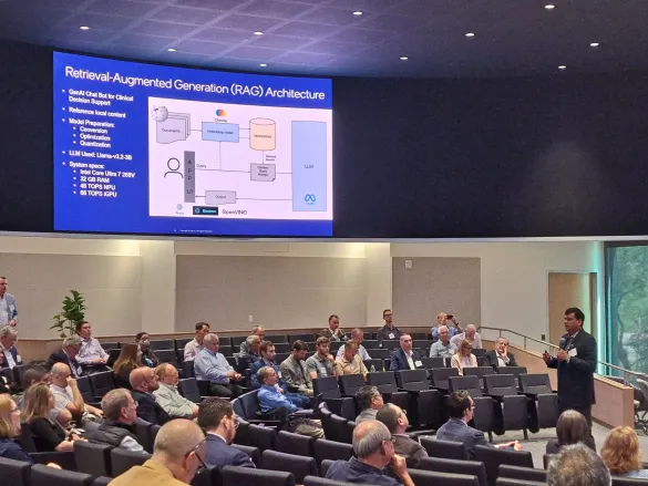
Designing functionally correct, high-performance, and provably secure system-on-chips (SoCs) has become a strategic imperative for modern computing infrastructure. Yet traditional design and verification methodologies are increasingly strained by escalating complexity, massive design scales, heterogeneous integration, and rapidly evolving security threats. Ensuring correctness, scalability, comprehensiveness, and adaptability across the full SoC lifecycle now exceeds the practical limits of conventional toolchains and human-centric workflows.
The emergence of large language models (LLMs) introduces a transformative opportunity for SoC design automation. Beyond natural language understanding and code generation, advanced LLMs demonstrate capabilities in architectural reasoning, specification refinement, vulnerability analysis, and design-space exploration. However, monolithic models alone are insufficient for the multidisciplinary and iterative nature of chip design. An agentic paradigm—where specialized LLM-driven agents collaborate within a coordinated framework—enables modular reasoning, cross-layer verification, security validation, and adaptive decision-making throughout the design process.
This talk will present a multi-agent intelligent assistant system architected to automate and augment SoC design and security verification. The framework integrates design synthesis, threat modeling, formal reasoning, runtime monitoring strategies, and hardware–software co-verification into a cohesive workflow. Looking ahead, such agentic systems point toward a future of self-optimizing, security-aware, and continuously verified silicon—where AI-driven design environments not only accelerate innovation but also fundamentally redefine how we conceive, build, and trust next-generation microelectronic systems.
United States
9:00 am
-
9:10 am
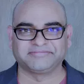
Warren Savage
Researcher
University of Maryland Applied Research Laboratory for Intelligence and Security
This webinar will present a multi-agent intelligent assistant system architected to automate and augment SoC design and security verification.
ESD Alliance Webinar: Gen-AI for Chip Design and Security
A Look Into the Future
9:00 am - 10:00 am
Off
Add to Calendar2026-09-10 09:00:002026-09-10 10:00:00ESD Alliance Webinar: Gen-AI for Chip Design and SecurityThis webinar will present a multi-agent intelligent assistant system architected to automate and augment SoC design and security verification.United StatesSEMI.org[email protected]America/Los_Angelespublic
America/Los_Angeles
Register Now
Standards meetings are open to all, but you must be a SEMI Standards Program Member to attend.
If you are not a Member, please register for the International SEMI Standards Program and start making a big contribution to the industry’s progress, complete an application form today!
Questions? Contact your local staff coordinator: Click here
1:30 pm - 3:00 pm
Off
Add to Calendar2026-06-19 13:30:002026-06-19 15:00:00Automation Technology Japan TC Chapter MeetingAutomation Technology Japan TC Chapter Meeting Date: Friday, June 19, 2025Time: 1:30 PM - 3:00 PM (JST)via Official Virtual TC Chapter Meeting + SEMI Japan (Hybrid)Please note that the meeting venue might be changed due to room capacity. If there is any change, we will inform you once it is confirmed. AGENDA Standards Contact Information:Nahoko KogaCoordinator, Standards & EHS, SEMI JapanEmail: [email protected] NOTE:Standards meetings are open to all, but you must be a SEMI Standards Program Member to attend.If you are not a Member, please register for the International SEMI Standards Program and start making a big contribution to the industry’s progress, complete an application form today! Questions? Contact your local staff coordinator: Click hereSEMI Japan 26F, xLINK Marunouchi Eiraku Bldg. 1-4-1 Marunouchi, Chiyoda-ku Chiyoda-ku, Tokyo 1000005 JapanSEMI.org[email protected]Asia/Tokyopublic
Asia/Tokyo
Standards meetings are open to all, but you must be a SEMI Standards Program Member to attend.
If you are not a Member, please register for the International SEMI Standards Program and start making a big contribution to the industry’s progress, complete an application form today!
Questions? Contact your local staff coordinator: Click here
2:00 pm - 4:00 pm
Off
Add to Calendar2026-06-05 14:00:002026-06-05 16:00:003D Packaging & Integration Japan TC Chapter Meeting3D Packaging & Integration Japan TC Chapter Meeting Date: Friday, June 5, 2026Time: 2:00 PM - 4:00 PM JSTvia OVTCCM/ SEMI Japan Office (Hybrid) AGENDA Standards Contact Information:Akiko YoshidaManager, SEMI JapanEmail: [email protected] NOTE:Standards meetings are open to all, but you must be a SEMI Standards Program Member to attend.If you are not a Member, please register for the International SEMI Standards Program and start making a big contribution to the industry’s progress, complete an application form today!Questions? Contact your local staff coordinator: Click hereSEMI Japan 26F, xLINK Marunouchi Eiraku Bldg. 1-4-1 Marunouchi Chiyoda-ku, Tokyo 1010005 JapanSEMI.org[email protected]Asia/Tokyopublic
Asia/Tokyo
This workshop is designed to help participants understand:
The real-world deployment, impact, and lessons learned from AI techniques
Strategies for building observable and scalable multi-agent workflows
The industry transition from restrictive data silos toward autonomous discovery.
Methods for achieving tangible business results and automation through diverse AI applications
We’ve curated a technical agenda featuring Topics such as:
Agentic AI
Gaussian Process Regression
Time Series Modeling
Bayesian Optimization
And more...
You will walk away with actionable insights on:
Yield Enhancement through Edge-Driven Defect Detection and Classification
Demonstrates how edge AI leverages real-time sensor and image data—through virtual metrology, anomaly detection, and SPC-integrated feedback loops—to enable early defect detection, classification, and yield optimization.
From Prediction to Action: Causal AI for Real-Time Root-Cause Analysis in Semiconductor Manufacturing
How causal AI unifies multi-modal fab data into an intelligence layer to move beyond predictive alerts toward rapid root cause identification, prescriptive actions, and continuous improvement—significantly reducing RCA time and improving yield and operational efficiency.
From Data Silos to Autonomous Discovery: Agentic AI in Semiconductors
Agentic AI in semiconductor workflows as autonomous, decision-making systems (beyond RAG) that orchestrate multi-agent reasoning across complex fab data—requiring robust data foundations, domain-grounded algorithms, SME-driven knowledge (including reasoning traces), and structured evaluation frameworks (agentic harness) to ensure reliable, scalable deployment.
Making Sense of Equipment Time‑Series Data: From Signals to Insight
Introduces how semiconductor equipment time-series data (sensor signals, traces, run-to-run data) can be processed and modeled to uncover equipment behavior over time, enabling engineers to detect drift, changes, and anomalies for improved monitoring and troubleshooting.
Achieving Business Results from Air-gapped Agentic AI Automation in Semiconductor Manufacturing - Lessons from the Field
Highlights real-world deployment of agentic AI in fabs, demonstrating how autonomous systems are driving yield, capacity, and operational gains across engineering workflows (FDC, yield, test, maintenance) while navigating constraints like data privacy and legacy integration—along with practical adoption strategies and hands-on use cases.
And more...
SEMI HQ 673 S Milpitas Blvd. Milpitas, CA95035 United States
Morning, Day 1: December 4, 2024
8:00 am
-
9:00 am
Registration & Breakfast
9:00 am
-
12:30 pm
Session #1 - Data Needs for Digital Twins - Data Sources, Integration & Interoperability
This session will explore the critical data requirements for creating and maintaining digital twins. Integrating multi-modal data sources (sensors, enterprise systems, equipment, etc.) that feed into digital twins, ensuring that they accurately reflect their physical counterparts is a minimum necessity. This session will also cover data integration techniques (from various factory systems), and interoperability to support dynamic digital twins.
9:00 am
-
9:10 am
Mark da Silva
Senior Director, Smart Manufacturing
SEMI
Welcome Remarks
9:10 am
-
9:35 am
Michael Neel
Director of Marketing
Inficon
Keynote - Enabling Autonomous Operations Through Integrated Digital Twins
9:35 am
-
10:00 am
Robert Baseman
Senior Technical Staff Member
IBM
Semantic Models for Microelectronic Manufacturing & Development
10:00 am
-
10:25 am
David McKee
Technology Leader & Managing Partner
Counterpoint Tech/DTC
Journey to Twins: A toolkit for Capabilities & Data to Digital Twins
10:25 am
-
10:40 am
Coffee Break - Sponsored by INFICON
10:40 am
-
11:05 am
Rad Desiraju
Director, WW Industry Advisory
Microsoft
Overcoming Data Interoperability Challenges for Effective Digital Twins
11:05 am
-
11:30 am
Wei Zhao
Head of Process Integration
Athinia
Chris Han-Adebekun
VP, Business Development
Athinia
Building Process & Supply Chain Digital Twins through Integrated Data Assets and Secure Data Sharing
11:30 am
-
12:30 pm
Dave Henshall
Vice President of Business Development and Government Relations
Semiconductor Research Corporation
Chris Ritter
CTO
Idaho National Lab
Special Session - SmartUSA – Semiconductor Digital Twin Manufacturing USA Institute
12:30 pm
-
2:00 pm
Lunch
Afternoon, Day 1: December 4, 2024
2:00 pm
-
5:00 pm
Session #2 - Data Standards for Digital Twins: Managing Unclean Factory Data
This session will focus on the importance of data standards for digital twins in semiconductor manufacturing, particularly in the context of dealing with unclean factory data. It will explore the challenges associated with unclean data and discuss strategies for cleaning and standardizing to ensure seamless ingestion into digital twins at various levels. Best practices for data validation, transformation, and integration as well as how to implement robust data standards to enhance reliability and accuracy of digital twins.
Sponsored by - Seeq
2:00 pm
-
2:25 pm
Dr. Joseph Ervin
Product Line Head of Semiverse Solutions Group
Lam Research
Keynote - Addressing Future Challenges in the Stochastics Era of Patterning with EUV Dry Resist
New patterning technologies will be needed to advance the device roadmap to 2 nm and beyond. Minimum pitch scaling will be exceptionally difficult to achieve at these advanced nodes, even with EUV patterning. Stochastic effects using wet resists during EUV patterning become problematic at the nanoscale, and can lead to line collapse, bridging, unacceptable line edge roughness (LER) and line width roughness (LWR). These stochastic effects present challenges when optimizing the tradeoffs between EUV resist resolution, dose, sensitivity, line edge / line width roughness, defectivity and cost.
In this talk, we will review the basics of dry resist technology, including dry resist equipment requirements, process flows and process integration modeling. In addition, we will present data that documents the advantages of dry resist technology over wet resist technology, demonstrating superior image quality, scaling and yield. We will conclude the talk by demonstrating a digital twin of the process integration and usage of optimization to achieve improved LER/LWR characteristics.
2:25 pm
-
2:50 pm
Alan Weber
Vice President, New Product Innovations
Cimetrix by PDF Solutions
Charting the Digital Twin Standardization Path: An Iterative Implementation and Abstraction Process
2:50 pm
-
3:15 pm
Brett Brimhall
Deloitte
3:15 pm
-
3:30 pm
Coffee Break - Sponsored by INFICON
3:30 pm
-
3:55 pm
Andres Torres
Engineer and Key Expert
Siemens
Feature Engineering as the bridge to Semantic Factory Data
3:55 pm
-
4:20 pm
Michael Bowcutt
Director of Sales Engineering for Romaric products at camLine
camLine USA
Control Software Integration with Digital Twins: How Virtual Data Aligns with Physical Reality
4:20 pm
-
5:20 pm
Moderator
Kenneth Smith
VP Growth Markets
Seeq
Sean Tropsa
Principal Analytics Engineer
Seeq
Panel: Harmonizing Standards for Semiconductor Digital Twins
5:30 pm
-
7:00 pm
Networking Reception - Sponsored by Sentient Cloud
Morning, Day 2: December 5, 2024
8:00 am
-
9:00 am
Registration & Breakfast
9:00 am
-
12:30 pm
Session #3 - Modeling High Complexity Semiconductor Processes
This session will explore the integration of digital twin technology in modeling high complexity semiconductor processes. As the semiconductor industry advances, the need for precise and efficient modeling techniques becomes crucial. Digital Twins offer a transformative approach to simulate and optimizes these processes, though challenges exist. Cases studies and future innovations will also be covered in this session.
9:00 am
-
9:05 am
Mark da Silva
Senior Director, Smart Manufacturing
SEMI
Welcome Remarks
9:05 am
-
9:30 am
Umesh Kelkar
Master/Vice President, Semiconductor Products Group
Applied Materials
Keynote: Key Enablers for Semiconductor Equipment and Process Digital Twins: Accelerated Computing (AC), Artificial Intelligence (AI) and Physics Modeling
9:30 am
-
9:55 am
Prith Bannerjee
Chief Technology Officer
Ansys
AI Driven Digital Twins for Semiconductor Manufacturing
9:55 am
-
10:20 am
Xi-Wei Lin
Executive Director, Applications Engineering
Synopsys
AI and Physics-based Models for Technological Development with High Complexity Semiconductor Processes
10:20 am
-
10:45 am
Coffee Break - Sponsored by PhysicsX
10:45 am
-
11:10 am
Amit Lal
Professor, Cornell University
Cornell
Peter Doerschuk
Professor
Cornell University
Ben Davaji
Assistant Professor
Northeastern University
Digital Twin Flow Using AI/ML Applied to Ferroelectric Memory
11:10 am
-
11:35 am
John Maculley
Semiconductor Industry Strategy Consultant
Dassault Systemes
Leveraging Virtual Twins and AI for Enhanced Fabrication Technology Co-Optimization in Semiconductor Manufacturing
11:35 am
-
12:30 pm
Pushkar Apte
Strategic Technology Advisor and Global Data-AI Lead
SEMI
Panel Discussion
12:30 pm
-
2:00 pm
Lunch - Sponsored by Dassault Systemes
Afternoon, Day 2: December 5, 2024
2:00 pm
-
5:00 pm
Session #4 - GenAI & AI/ML Role in the Development of Digital Twins - Implementation Strategies for DT
Integrating AI/GenAI & Digital Twins - Explore the cutting-edge integration of Generative AI (GenAI) and Artificial Intelligence/Machine Learning (AI/ML) in the creation and evolution of digital twins. This session will delve into how GenAI & AI/ML technologies are revolutionizing the simulation, prediction, and real-time replication of physical assets in semiconductors through case studies and practical applications.
2:00 pm
-
2:25 pm
Kamaljeet Ghotra
Senior Director, Go-To Market and Digital Strategy
PDF Solutions
Keynote - Accelerating Digital Twins with Gen AI
The rise of sophisticated AI tools, including generative AI, is revolutionizing the semiconductor industry by enabling the analysis of vast datasets to generate valuable insights. Executives in the sector see generative AI as a transformative force rather than just another tool. They believe it can deliver significant value, particularly in manufacturing, operations, and maintenance, its potential for process and equipment analysis, Predictive maintenance and smart diagnostics.
As fabs adopt smart manufacturing and virtual modeling it is pertinent for digital twins to leverage technologies like generative AI for data generation, Data Synthesis/Augmentation, Real Time Analysis, Model Optimization (AI enhanced physics models) , Rapid Prototyping and Accelerated Design and Development with data-driven model-based learning.
2:25 pm
-
2:50 pm
Peter Lendermann
CTO
D-SIMLAB
About Cross-Fertilization between Digital Twins and AI Techniques for Capacity Planning and WIP Flow Optimisation in Semiconductor Fabs
2:50 pm
-
3:15 pm
Kiran Karunakaran
Chief Technology Officer
Via Automation
Developing Explainable Digital Twins for the Semiconductor Industry Using GenAI, Knowledge Graphs, and ML Techniques
3:15 pm
-
3:30 pm
Coffee Break - Sponsored by PhysicsX
3:30 pm
-
3:55 pm
Mark Huntington
Managing Director of North America
PhysicsX
Real-Time Digital Twins for Semiconductor Manufacturing: Accelerating Multi-Physics Optimization with Physics-Based AI
3:55 pm
-
4:20 pm
Becky Kelderman
Solutions Sales Manager
Rockwell Automation
Advancing Industrial Data Architectures & Models for AI in Process Digital Twins
4:20 pm
-
5:20 pm
Moderator
Mithun Kamat
Partner
McKinsey
Panel - Rewiring organizations for AI / Digital twin: a business-backed view of successful implementation and challenges in adoption of Digital twins in the semiconductor industry
The SEMI Smart Manufacturing Initiative is hosting a two-day workshop titled "AI Techniques in Semiconductor Manufacturing" at SEMI HQ in Milpitas, CA, on August 5–6, 2026. This event is part of a continuing series focused on integrating advanced AI into the semiconductor landscape. The workshop is designed to help participants understand: The real-world deployment, impact, and lessons learned from AI techniques. Strategies for building observable and scalable multi-agent workflows. The industry transition from restrictive data silos toward autonomous discovery. Methods for achieving tangible business results and automation through diverse AI applications.
AI Techniques in Semiconductor Manufacturing
[IN-PERSON EVENT]
Aug 5-6, 2026
8:00 am - 5:00 pm
Off
Add to Calendar2026-08-05 08:00:002026-08-06 17:00:00AI Techniques in Semiconductor Manufacturing The SEMI Smart Manufacturing Initiative is hosting a two-day workshop titled "AI Techniques in Semiconductor Manufacturing" at SEMI HQ in Milpitas, CA, on August 5–6, 2026. This event is part of a continuing series focused on integrating advanced AI into the semiconductor landscape. The workshop is designed to help participants understand: The real-world deployment, impact, and lessons learned from AI techniques. Strategies for building observable and scalable multi-agent workflows. The industry transition from restrictive data silos toward autonomous discovery. Methods for achieving tangible business results and automation through diverse AI applications.SEMI HQ 673 S Milpitas Blvd. Milpitas, CA 95035 United StatesSEMI.org[email protected]America/Los_Angelespublic
America/Los_Angeles
Register Now
Cancellation request received on or before August 12 will be eligible for a refund. After this date, only substitutions will be accepted. Please email your cancellation request to AgnesCobar at [email protected]. Substitutions will only be accepted with written permission from the originally registered attendee.
Artificial intelligence (AI) continues to grow rapidly, driving unprecedented transformation. And for all the hype, the best is yet to come! But AI's energy footprint is growing rapidly and the global “data center gold rush” is already straining energy grids and natural resources around the world. This is a formidable challenge that cannot be ignored.
For industry, this is a strategic business imperative. AI access costs are mounting, and there is increasing stakeholder pressure to show ROI on AI investments. Competitive advantage derives from running AI systems as efficiently as possible, maximizing performance and minimizing energy consumption. And for the next big application of physical AI, efficiency becomes absolutely critical.
No entity can address this alone. The SEMI Smart Data-AI Initiative has been working to build a meaningful collaboration across the entire AI ecosystem to “bend the curve.” In this workshop, together with our alliance partner San Jose, we bring together distinguished leaders across the spectrum to share insights and chart the future course. Please join us at this exciting interactive event.
Mexican Heritage Plaza 1700 Alum Rock Ave San Jose, CA95116 United States
From AI to Quantum, the Future is Now in California
9:45 am
-
10:05 am
David Fried
Chief AI Officer & Corporate VP
Lam Research
Keynote: Lam Research
10:05 am
-
10:25 am
Dr. Mahmut Ersin Sinangil
Distinguished Research Scientist
NVIDIA
Keynote: NVIDIA
10:25 am
-
10:45 am
Yvonne Ferrier
Associate Principal
McKinsey & Co
Keynote: McKinsey & Co
Unlocking Efficient AI Inference at Scale
Break
10:45 am
-
11:05 am
Networking Coffee Break
11:05 am
-
11:10 am
Gity Samadi
Sr. Director R&D Programs
SEMI
Session Introduction: SEMI
11:10 am
-
11:30 am
Vikrant Lal
Fellow
Optical Networks Division
Session Keynote: Nokia
At the Intersection of Photonics Innovation and AI's Energy Challenge
11:30 am
-
12:15 pm
Panel Discussion
Photonics Panel - System Technology Co-Optimization – Chair, Gity Samadi
• Nokia – Vikrant Lal
• Aelumna - Jonathan Klamkin, CEO
• Avicena – Nigel Alvares, VP of Product & Marketing
• Veeco – Peter Porshnev, CTO
• ASE - Speaker TBD
Networking Break
12:15 pm
-
1:30 pm
Lunch
1:30 pm
-
1:40 pm
Melissa Grupen-Shemansky
VP & CTO
SEMI
Introduction to SEMI Technology Coalitions and Afternoon Sessions
1:40 pm
-
2:00 pm
Christopher Wellise (CW)
VP-Sustainability
Equinix
Session Keynote: Equinix
2:00 pm
-
2:10 pm
Sundeep Bajikar
CVP Corporate Strategy & Marketing
Applied Materials
Panel Introduction: Applied Materials
Chip-to-Grid
2:10 pm
-
3:00 pm
Chip-to-Grid Panel
Panel Discussion – Chair, Sundeep Bajikar
• Equinix - Christopher Wellise (CW), VP-Sustainability
• City of San Jose Erica Garaffo, Large-Load Energy Cust. Dev. Lead.
• PG&E - Karen Khamou Ornelas, Data Center Power Supply Mgmt
• Deloitte, Craig Lobdell, Senior Manager
Networking Break
3:00 pm
-
3:20 pm
Coffee Break
3:20 pm
-
3:40 pm
Nuwan Jayasena
Fellow
AMD
Session Keynote: AMD
Managing Memory Architecture
3:40 pm
-
4:00 pm
Cliff Young
TPU & Anton Architect, MLPerf co-founder
Google
Session Keynote: Google
Bounded Revolutionary Jumps
4:00 pm
-
4:45 pm
Efficient Systems Panel Discussion
Panel Discussion – Chair, Pushkar Apte
• Google – Cliff Young
• AMD – Nuwan Jayasena
• SK Hynix – John Kim
• Siemens/Mentor – Mark Malinoski
• Qualcomm - Vinish Sukumar, VP & AI Product Mgmt Head
Bending the Curve for Power & Performance [In-Person Event]
8:00 am - 6:45 pm
Off
Add to Calendar Disabled
America/Los_Angeles
Alliance Partner
The SEMI Smart Data-AI Initiative is organizing this workshop with our Alliance Partner, the City of San Jose. We are uniting the entire AI ecosystem including devices, materials, packaging, photonics, quantum, architectures and algorithms. Please join us in this exciting interactive workshop.
Standards meetings are open to all, but you must be a SEMI Standards Program Member to attend.
If you are not a Member, please register for the International SEMI Standards Program and start making a big contribution to the industry’s progress, complete an application form today!
Questions? Contact your local staff coordinator: Click here
Liquid Chemicals Japan TC Chapter Meeting
3:30 pm - 5:30 pm
Off
Add to Calendar2026-05-21 15:30:002026-05-21 17:30:00Liquid Chemicals Japan TC Chapter MeetingLiquid Chemicals Japan TC Chapter Meeting Date: Thursday, May 21, 2026Time: 3:30 pm - 5:30 pm JSTVenue: SEMI Japan Office + OVTCCM (Hybrid) AGENDA Standards Contact Information:Takeaki HirabaraStandards & EHS, SEMI JapanEmail: [email protected] NOTE:Standards meetings are open to all, but you must be a SEMI Standards Program Member to attend.If you are not a Member, please register for the International SEMI Standards Program and start making a big contribution to the industry’s progress, complete an application form today!Questions? Contact your local staff coordinator: Click hereSEMI Japan 26F, xLINK Marunouchi Eiraku Bldg. 1-4-1 Marunouchi Chiyoda-ku, Tokyo 1000005 JapanSEMI.org[email protected]Asia/Tokyopublic
Asia/Tokyo
Standards meetings are open to all, but you must be a SEMI Standards Program Member to attend.
If you are not a Member, please register for the International SEMI Standards Program and start making a big contribution to the industry’s progress, complete an application form today!
Questions? Contact your local staff coordinator: Click here
Physical Interfaces & Carriers Japan TC Chapter Meeting
9:00 am - 12:00 pm
Off
Add to Calendar2026-05-21 09:00:002026-05-21 12:00:00Physical Interfaces & Carriers Japan TC Chapter MeetingPhysical Interfaces & Carriers Japan TC Chapter Meeting Date: Thursday, May 21, 2026Time: 9:00 am - 12:00 pm JSTVenue: Room 102 @ Otemachi PLACE HALL & CONFERENCE + OVTCCM (Hybrid) AGENDA Standards Contact Information:Takeaki HirabaraStandards & EHS, SEMI JapanEmail: [email protected] NOTE:Standards meetings are open to all, but you must be a SEMI Standards Program Member to attend.If you are not a Member, please register for the International SEMI Standards Program and start making a big contribution to the industry’s progress, complete an application form today!Questions? Contact your local staff coordinator: Click hereOtemachi PLACE HALL & CONFERENCE Otemachi PLACE East Tower 2-3-1 Otemachi, Chiyoda-ku, Tokyo 1000004 JapanSEMI.org[email protected]Asia/Tokyopublic
Asia/Tokyo
This comprehensive course will cover the underlying fundamentals, the interrelationship between materials and processes, and the hardware used in printed electronics. The masterclass will also explore how printed electronics can be applied currently in example applications including practical aspects of the technology, its highlights and challenges and scalability. We will also explore emerging new technologies at the cutting edge of FHE, semiconductor packaging, photonics and quantum materials. Throughout the course there will be opportunities for Q/A and discussions and case studies based on participant's interest.
ABOUT THE SPEAKER
J. Devin MacKenzie, PhD Dr. Devin MacKenzie is the Washington Research Foundation Professor and an Assoc. Prof. of Materials Science and Engineering and Mechanical Engineering at UW. He is also the Technical Director of the Washington Clean Energy Testbeds, a lab that provides open-access to world-class advanced manufacturing and characterization tools for printed optoelectronics, sensors and energy device research and scale-up. Devin also has 25 years of entrepreneurial experience in sustainable materials and manufacturing of semiconductors, optoelectronics and energy devices. Prior to UW he was CEO and co-founder of printed battery company, Imprint Energy (acquired CCL/Avery), Previously, as the CTO of Add-Vision, Inc. (acquired Sumitomo Chemical), Dr. MacKenzie led R&D for roll-to-roll printed flexible OLEDs at Add-Vision with licensing in Europe and Asia. Prior to Add-Vision, he led printed silicon RF device and product engineering at Kovio, Inc. a Si Valley MIT spin-out (acquired Thin Film Electronics). Dr. MacKenzie also co-founded, Plastic Logic, from Cambridge University as a postdoc and subsequently a visiting scientist in Physics at the Cavendish Laboratory. Prior to that he worked at Bell Labs and NASA. Dr. MacKenzie has authored over 240 publications and patents that have been licensed globally and has been cited over 12,900 times in fields ranging from rare earth-doped nitrides to quantum materials. He holds Ph.D, MS, and undergraduate degrees in Materials Science and Engineering from the University of Florida and the Massachusetts Institute of Technology.
United States
J. Devin MacKenzie, PhD
Washington Research Foundation Professor of Clean Energy, Associate Professor
Join us for a comprehensive Master Class with Dr. Devin MacKenzie, as he dives into the fundamentals and real-world applications of printed and flexible hybrid electronics (FHE). This session will explore the critical interrelationship between materials, processes, and hardware used in printed electronics, providing a strong foundation for understanding how these systems are designed and manufactured.
Participants will gain insight into current applications of printed electronics, along with practical considerations such as performance, scalability, and manufacturing challenges. The course will also highlight emerging technologies at the forefront of innovation, including advances in FHE, semiconductor packaging, photonics, and quantum materials
Advancing Printed Electronics Technology: From Macroelectronics to Quantum Devices
Flexible Electronics Master Class #31
10:00 am - 12:00 pm
Off
Add to Calendar2026-09-30 10:00:002026-09-30 12:00:00FEMC#31 Advancing Printed Electronics Technology: From Macroelectronics to Quantum DevicesJoin us for a comprehensive Master Class with Dr. Devin MacKenzie, as he dives into the fundamentals and real-world applications of printed and flexible hybrid electronics (FHE). This session will explore the critical interrelationship between materials, processes, and hardware used in printed electronics, providing a strong foundation for understanding how these systems are designed and manufactured.Participants will gain insight into current applications of printed electronics, along with practical considerations such as performance, scalability, and manufacturing challenges. The course will also highlight emerging technologies at the forefront of innovation, including advances in FHE, semiconductor packaging, photonics, and quantum materialsUnited StatesSEMI.org[email protected]America/Los_Angelespublic
America/Los_Angeles
REGISTER NOW
Join the SEMI Water Management team and document authors for a webinar discussing their research and findings for the Water Management Strategy Reports. The reports are guides for water managers for understanding their water balance, baseline, potential savings and a general maturity scale for several solutions to be considered to move up the maturity scale to Zero Liquid Discharge (ZLD). The webinar will provide an overview on how the documents should be used to work with water solutions providers and provide strategies for both new and legacy facilities with end-of-pipe solutions as well as treatments for individual process stage water discharge.
The webinar will include a discussion of next steps for the continued development of the reports, including how they interact with SEMI Standards and the industry roadmaps.
9:00 am - 10:00 am
Off
Add to Calendar2026-05-21 09:00:002026-05-21 10:00:00Water Management Strategies WebinarJoin the SEMI Water Management team and document authors for a webinar discussing their research and findings for the Water Management Strategy Reports. The reports are guides for water managers for understanding their water balance, baseline, potential savings and a general maturity scale for several solutions to be considered to move up the maturity scale to Zero Liquid Discharge (ZLD). The webinar will provide an overview on how the documents should be used to work with water solutions providers and provide strategies for both new and legacy facilities with end-of-pipe solutions as well as treatments for individual process stage water discharge. The webinar will include a discussion of next steps for the continued development of the reports, including how they interact with SEMI Standards and the industry roadmaps.Reports can be downloaded HERE.United StatesSEMI.org[email protected]America/Los_Angelespublic
America/Los_Angeles
Register Here
Cancellations received on or before July 27, 2026, are fully refunded with a $50 processing fee. Refunds will not be issued for cancellations (including no-shows) made after July 27, 2026, and only substitutions are accepted with a written note from the registered attendee. Please email your cancellations or substitutions on company letterhead to [email protected].
From integration to intervention: the whole is greater than the sum of its parts.
Healthcare is rapidly entering an era where nearly every physiological parameter can be measured. Though there has been a proliferation of advanced sensors, improved sensing alone has not consistently translated into meaningful improvement in outcomes. This talk highlights the opportunity to strengthen clinically-relevant integration and implementation across the health-technology ecosystem—from sensors platforms to analytics, workflows, and clinical care delivery. It touches on how advances in interoperability, contextualized data interpretation, workflow-aware design, and validation strategies can help translate clinically relevant measurement into meaningful, actionable intervention.
11:10 am
Panel Discussion
Panel discussion around integration.
12:00 pm
-
1:00 pm
Lunch
Innovation
1:00 pm
-
1:20 pm
Gregg Bartlett
Chief Technology Officer
GlobalFoundries
Presentation - GlobalFoundries
Gregg Bartlett, CTO GlobalFoundries
1:20 pm
-
1:40 pm
Pieris Berreitter
Director of Engineering
HP
Presentation
Pieris Berreitter, HP
1:40 pm
-
2:00 pm
Mauro Ferrari
Chief Executive Officer
BrYet
Presentation
Mauro Ferrari, CEO BrYet
2:00 pm
-
2:45 pm
Panel Discussion
2:45 pm
-
3:00 pm
Break
3:00 pm
-
3:15 pm
Bharat Rajagopalan
Director of Strategic Marketing
ST Microelectronics
Presentation
Bharat Rajagopalan, Director of Strategic Marketing ST Microelectronics
This Smart MedTech Summit brings together semiconductor and medical device leaders to address shared challenges, strengthen supply chain collaboration, and enable the next generation of medical devices. Designed for leaders at the forefront of a rapidly evolving landscape, it provides a focused forum for dialogue and cross-industry collaboration. Participants will engage with peers and experts to exchange perspectives and gain actionable insights into how advanced semiconductor technologies are enabling smarter, more connected medical solutions.
Semiconductor-MedTech Ecosystem Summit
A Smart MedTech event sponsored by GlobalFoundries
8:00 am - 6:00 pm
Off
Add to Calendar2026-08-27 08:00:002026-08-27 18:00:00Semiconductor-MedTech Ecosystem SummitThis Smart MedTech Summit brings together semiconductor and medical device leaders to address shared challenges, strengthen supply chain collaboration, and enable the next generation of medical devices. Designed for leaders at the forefront of a rapidly evolving landscape, it provides a focused forum for dialogue and cross-industry collaboration.Participants will engage with peers and experts to exchange perspectives and gain actionable insights into how advanced semiconductor technologies are enabling smarter, more connected medical solutions. SEMI Headquarters 673 S. Milpitas Boulevard Milpitas, CA 95035 United StatesSEMI.org[email protected]America/Los_Angelespublic