downloadGroupGroupnoun_press release_995423_000000 copyGroupnoun_Feed_96767_000000Group 19noun_pictures_1817522_000000Member company iconResource item iconStore item iconGroup 19Group 19noun_Photo_2085192_000000 Copynoun_presentation_2096081_000000Group 19Group Copy 7noun_webinar_692730_000000Path
Skip to main content
Default Banner Image

Business

Registration

Group Discounts Codes—

  • SMC3 - Register 3: 15% off (must register all 3 on same order)
  • SMC5 - Register 5: 20% off (must register all 5 on same order)
  • SMC10 - Register 10: 25% off (must register all 10 on same order)

NOTE:  For Group Discounts, Attendees must be registered within the same order.

For more information, please contact Karen Popp, Senior Program Manager, at [email protected].

Registration is final. Cancellations will not be accepted. No refunds provided. Substitutions are only accepted with written permission from the original registrant.

+
United States REGISTER NOW SEMI SMC Strategic Materials Conference Business Executive

Hotel

SMC24 Hayes Mansion San Jose Photo

HAYES MANSION
200 Edenvale Avenue
San Jose, CA, CA 95136

Book your hotel room before the link expires on June 26, 2026.


HEALTH & SAFETY

Your health and safety are our top priority. The personal preference of the attendees to wear masks is respected at all SEMI events. SEMI Americas (“SEMI") monitors developing federal, state, and local health and safety recommendations as well as requirements regarding COVID to determine the most appropriate safety protocols for our in-person events.

SMC24 Hayes Mansion San Jose Photo

Gold

Edwards Vacuum Logo 170x65
EFC Gases & Advanced Materials NEW
Huntsman

Silver

Applied Materials
Lam Research
SCREEN Logo 170x65

Event

EMD Electronics Logo 170x65
Entegris 170x65
JSR Micro
Mitsubishi Chemical Group Logo 170x65
Sundt

BECOME A SPONSOR FOR SMC

Sponsorship opportunities can be tailored to meet your specific branding and marketing objectives. Become a sponsor and brand your company to an influential audience at SMC.


CONTACT

Shane Poblete
Director, Sales & Business Development - Expo and Events, SEMI
Tel: +1 202-847-5983
Email: [email protected]

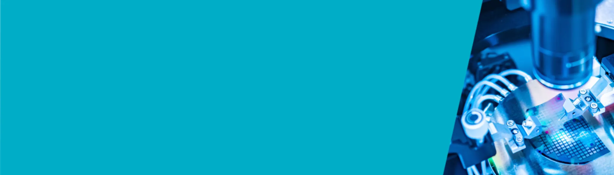
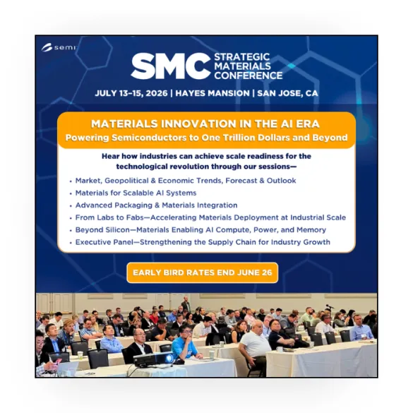
Materials Innovation in the AI Era: Powering Semiconductors to One Trillion Dollars and Beyond

Beyond the AI boom lies a challenge—and opportunity—that is far more foundational: ensuring the materials ecosystem underpinning a $2.5 trillion industry is resilient enough to support the next era of innovation. As artificial intelligence accelerates demand for advanced hardware, energy infrastructure, and high‑performance components, the pressure on global materials supply chains has never been greater.

This year, SMC explores how industries can achieve scale readiness through smarter design, diversified sourcing, sustainable processes, and breakthrough materials science. It invites leaders to look past the excitement of AI itself and toward the essential building blocks that will determine whether this technological revolution is secure and sustainable.

The Strategic Materials Conference—SMC offers valuable content and unprecedented networking opportunities for semiconductor industry professionals who share common strategic objectives on materials innovation, management, and business success. 

Sessions

  • ​Market, Geopolitics & Outlook 
  • ​Materials for Scalable AI Systems​
  • Advanced Packaging & Materials Integration​
  • From Labs to FabsAccelerating Materials Deployment at Industrial Scale
  • ​Quantum & Emerging Devices

Executive Panel–Strengthening the Supply Chain​

REGISTRATION INCLUDES

  • Approved speaker PDF presentations
  • Breakfast, lunch, coffee breaks
  • Two networking receptions
  • Tabletop exhibits

WHO SHOULD ATTEND

SMC offers valuable content and unprecedented networking opportunities for semiconductor industry professionals who share common strategic objectives on materials innovation, management, and business success. 

CEO  ●  CTO  ●  Presidents & General Managers  ●  Executive VP & Senior Executives  ●  Engineering & Fab Managers ●  Academia  ●  Startup Founders  ●  Financial Analysts  ●  Market Researchers  ●  Consulting Firms  ●  Consortiums
 

2026 ORGANIZING COMMITTEE
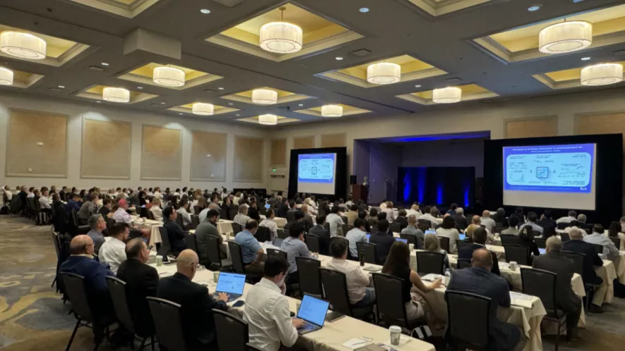
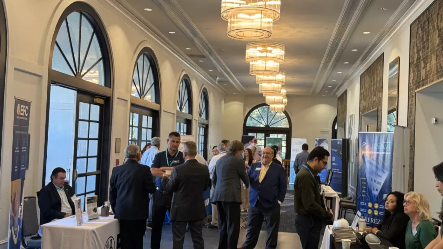
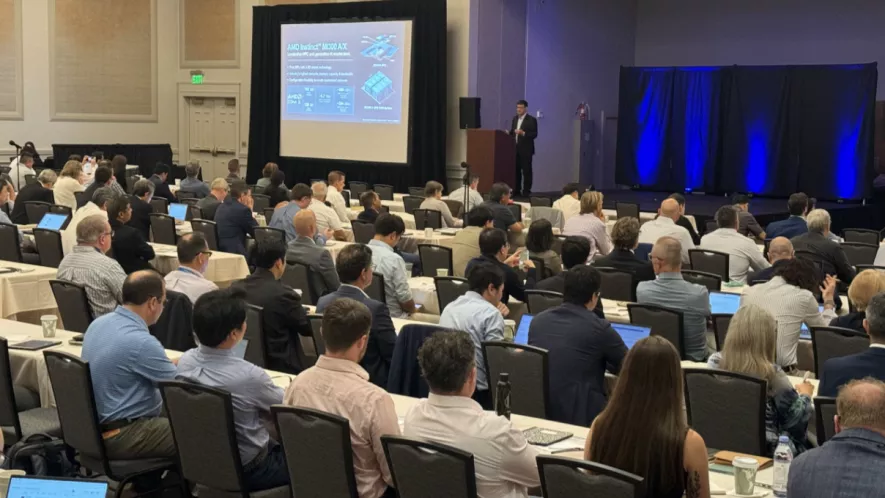
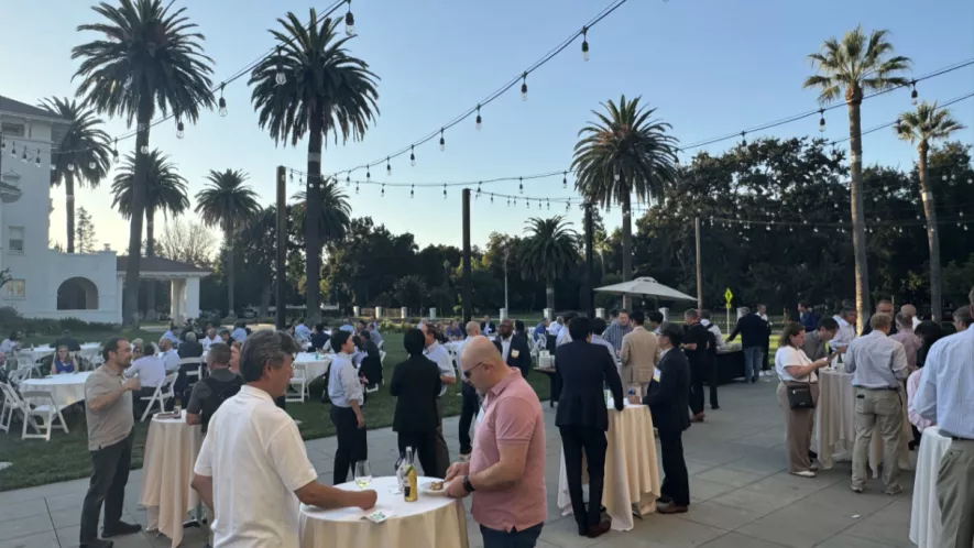
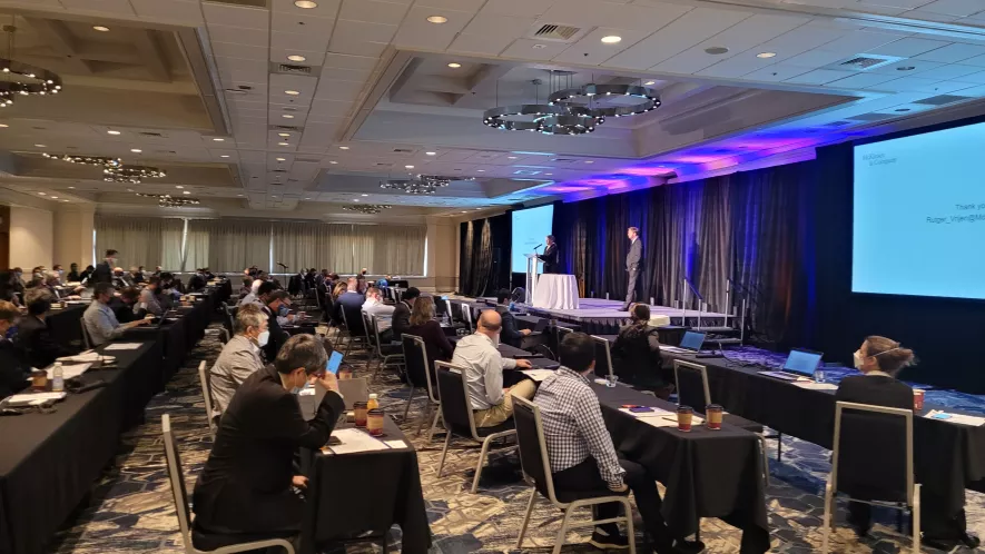
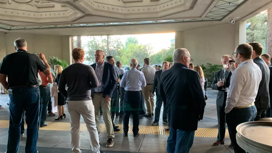
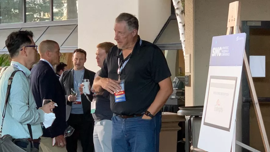
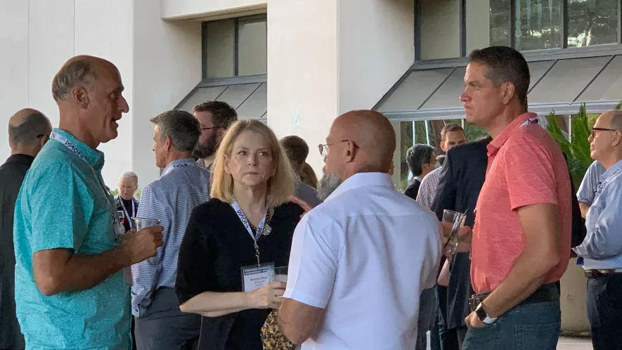
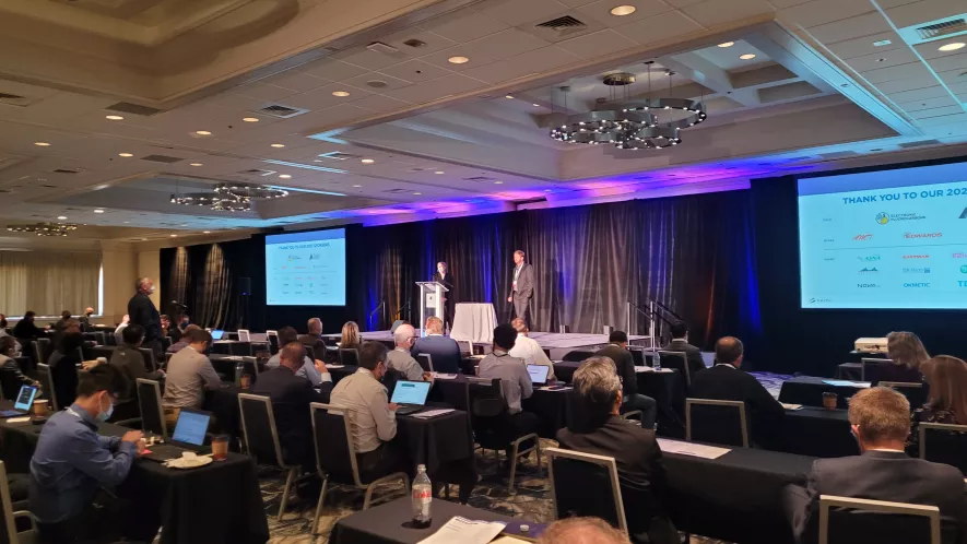
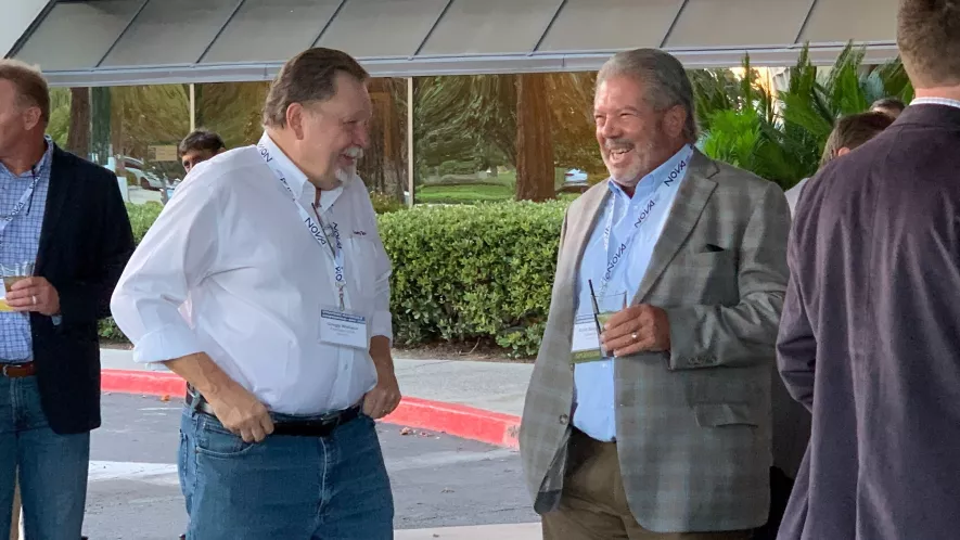
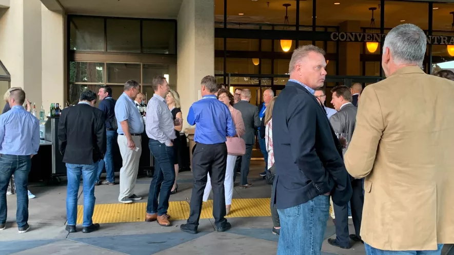
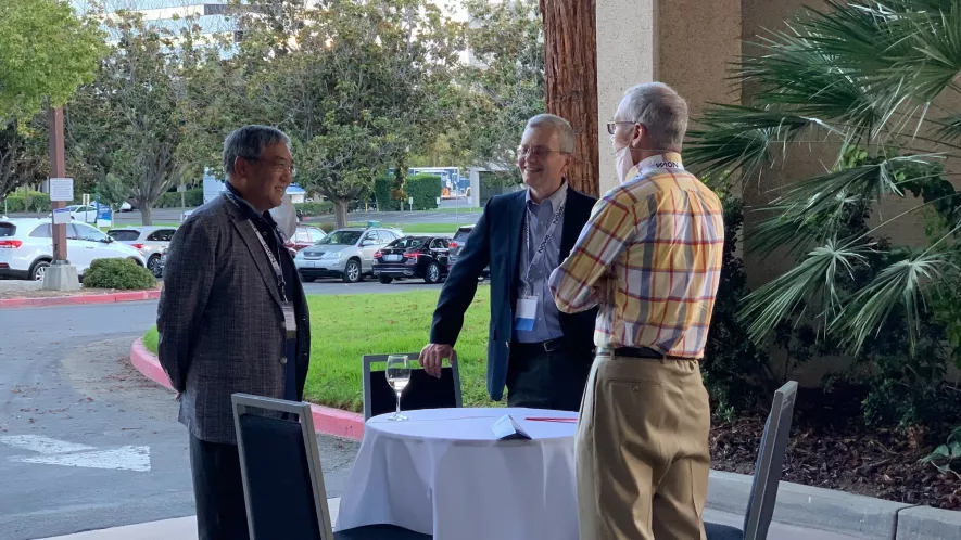
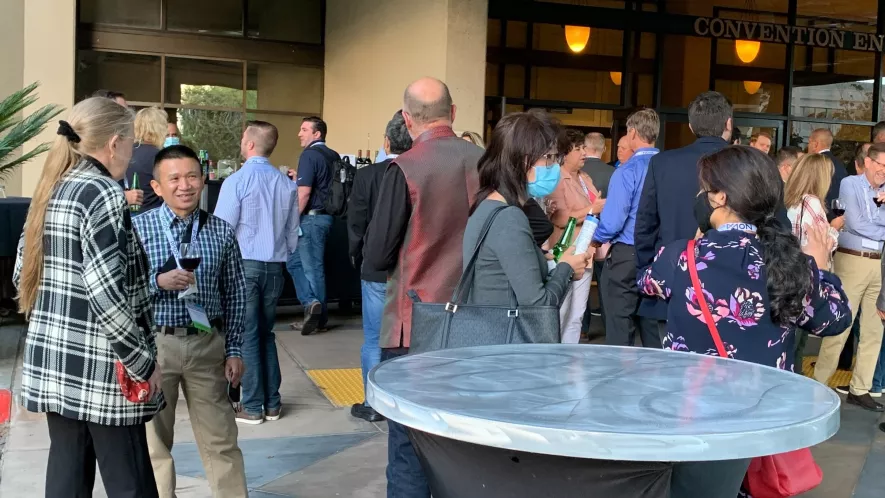
SMC Photo Gallery

Hayes Mansion
200 Edenvale Avenue
San Jose, CA, CA 95136
United States

MONDAY, JULY 13, 2026

5:30 pm - 7:00 pm

Welcome Reception

Entegris 170x65
Joe Stockunas, SEMI Americas
Joe Stockunas
President
SEMI Americas

Welcome Remarks

TUESDAY, JULY 14, 2026

8:00 am - 8:30 am

Registration, Check-In/Continental Breakfast

Mitsubishi Chemical Group Logo 170x65
8:30 am - 8:40 am
Joe Stockunas, SEMI Americas
Joe Stockunas
President
SEMI Americas

Welcome Remarks

8:40 am - 8:50 am
Sanjiv Bhatt, Mitsubishi
SMC Co-Chair
Sanjiv Bhatt
Director, OEM
Mitsubishi Chemical Advanced Materials

Opening Remarks

8:50 am - 9:20 am
Hideaki Okamoto, Mitsubishi Headshot
Hideaki Okamoto
Director, New Generation Business Development
Mitsubishi Chemical

Keynote—A Strategic Approach in the Era of Materials Innovation

9:20 am - 9:50 am
Prahalad Parthangal, Lam Research
Prahalad Parthangal, PhD
Technical Director, Advanced Packaging
Lam Research

Keynote—Co-Engineering the AI Era: How Materials, Process and Equipment Innovations Converge in Advanced Packaging

9:50 am - 10:20 am

Networking Break

JSR Micro

Session 1—Market, Geopolitical & Economic Trends, Forecast & Outlook

10:20 am - 10:25 am
Aldo Orsi, Momentive Technologies
Aldo Orsi
Global Business Director, Quartz Solids
Momentive Technologies

Opening Remarks

Sundt
10:25 am - 10:55 am
Charles Shi, Needham & Company
Charles Shi, PhD
Managing Director
Needham & Company
11:25 am - 11:55 am
Joe Stockunas, SEMI Americas
Joe Stockunas
President
SEMI Americas

News from Washington and Beyond

11:55 pm - 1:15 pm

Lunch

Mitsubishi Chemical Group Logo 170x65

Session 2—Materials for Scalable AI Systems

1:15 pm - 1:20 pm
Lu Gan, EMD Electronics
Lu Gan, PhD
Head of Technology Strategy & Roadmap
EMD Performance Materials, a subsidiary of Merck KGaA

Opening Remarks

EMD Electronics Logo 170x65
1:20 pm - 1:50 pm
Katherine Hutchinson, EMD Electronics
Katherine Hutchinson, PhD
Vice President and General Manager, Metallics, Thin Film Business
EMD Electronics

Materials Discovery in the Era of Scientific Super Intelligence

1:50 pm - 2:20 pm
Mark O'Neill, Entegris
Mark O'Neill
Vice President, R&D and Engineering
Entegris

Taming AI Scaling Stresses—Digital Materials Discovery for Manufacturing-Ready Adoption

2:20 pm - 2:50 pm
Mingqi Li, Qnity Electronics
Mingqi Li, PhD
Technical Fellow
Qnity Electronics

Pioneering Lithographic Materials for the AI Era—Next Generation EUV materials and Path to Sustainable Patterning

2:50 pm - 3:20 pm

Networking Break

3:20 pm - 3:50 pm
Chris Baldwin, Boston Materials
Chris Baldwin
Vice President, Product
Boston Materials

Thermal Materials Implications of the Explosion in AI Compute Demand

Session 3—Advanced Packaging & Materials Integration

3:50 pm - 3:55 pm
Kamran Akhtar, Samsung Semiconductor
Kamran Akhtar, PhD
Senior Director, Process Development
Samsung

Opening Remarks

3:55 pm - 4:25 pm
Sony Varghese, Applied Materials
Sony Varghese
Managing Director
Applied Materials

Materials Engineering for Improved Stacking in HBM and Chiplet Integration

4:25 pm - 4:55 pm
Kazuyuki Mitsukura, Resonac
Kazuyuki Mitsukura, PhD
Technical Director
Resonac America
4:55 pm - 5:25 pm
Rozalia Beica, Rapidus Design Solutions
Rozalia Beica
Field CTO, Packaging Technologies
Rapidus Design Solutions

Advanced Packaging at the Heart of the AI Age

5:25 pm - 6:30 pm

Networking Reception

WEDNESDAY, JULY 15, 2026

7:30 am - 8:00 am

Registration, Check-In/Continental Breakfast

8:00 am - 8:05 am
Arun Karamcheti, Applied Materials
SMC Co-Chair
Arun Karamcheti, PhD
Managing Director, Product Marketing and Strategy
Applied Materials

Opening Remarks

8:05 am - 8:35 am
Beth Adkison, Intel
Beth Adkison
Senior Director, Global Materials Organization
Intel

Keynote—From Innovation to Scale: Ramp Readiness in the AI Era

8:35 am - 9:05 am
Chuck Mattera, Avalanche Thinking
Chuck Mattera, PhD
Founder and CEO
Avalanche Thinking

Keynote—Compound Semiconductors in the Cognitive Age

Session 4—From Lab to Fab—Accelerating the Industrialization of Next Generation Materials Deployment and Manufacturing

9:05 am - 9:10 am

Opening Remarks

9:10 am - 9:40 am
Mitchell Hsing, InchFab
Mitchell Hsing, PhD
Co-Founder and CEO
InchFab

How Democratizing Fab Enables Rapid Innovation

9:40 am - 10:10 am
Adrian Alvarez, RASIRC
Adrian Alvarez
Business Development Director, Deputy CTO
RASIRC

The Hedgehog and the Fab

10:10 am - 10:40 am

Networking Break

10:40 am - 11:10 am
Asif Khan, Georgia Institute of Technology
Asif Khan, PhD
Associate Professor, School of Electrical and Computer Engineering
Georgia Institute of Technology

Lab to Fab—Accelerating the Industrialization of Next Generation Materials and Manufacturing

11:10 am - 11:40 am
Brian Larabee, General Graphene
Brian Larabee
Chief Commercial Officer
General Graphene
11:40 am - 12:40 pm

Lunch

Session 5—Quantum and the Future of Emerging Devices

12:40 pm - 12:45 pm
Kevin Peterson
Kevin D. Peterson
Vice President, Sales and Marketing
JX Nippon Mining & Materials

Opening Remarks

12:45 pm - 1:15 pm
Pooya Tadayon, Ayar Labs
Pooya Tadayon, PhD
VP and Senior Fellow
GlobalFoundries

Enabling Quantum Computing Through Advanced Packaging

1:15 pm - 1:45 pm
Elica Kyoseva, NVIDIA
Elica (Elitsa) Kyoseva
Director, Quantum Algorithm Engineering
NVIDIA

Defining the Quantum-GPU Supercomputer

1:45 pm - 2:15 pm
Percy Gilbert, PhD, SkyWater Technology
Percy Gilbert, PhD
Senior Vice President, Engineering
SkyWater Technology

Industrializing the Next Compute Era—From Materials to Manufacturing

2:15 pm - 2:45 pm

Networking Break

Session 6—Executive Panel: Strengthening the Supply Chain for Industry Growth

2:45 pm - 2:50 pm

Opening Remarks

2:50 pm - 4:00 pm
Wenge Yang, Entegris
MODERATOR
Wenge Yang
Vice President, Market Strategy
Entegris
Chuck Mattera, Avalanche Thinking
Chuck Mattera, PhD
Founder and CEO
Avalanche Thinking
Brian Larabee, General Graphene
Brian Larabee
Chief Commercial Officer
General Graphene
Pooya Tadayon, Ayar Labs
Pooya Tadayon, PhD
VP and Senior Fellow
GlobalFoundries
Beth Adkison, Intel
Beth Adkison
Senior Director, Global Materials Organization
Intel
Prahalad Parthangal, Lam Research
Prahalad Parthangal, PhD
Technical Director, Advanced Packaging
Lam Research
4:00 pm - 4:10 pm
Arun Karamcheti, Applied Materials
SMC Co-Chair
Arun Karamcheti, PhD
Managing Director, Product Marketing and Strategy
Applied Materials

Closing Remarks

- APHI EMG Off Add to Calendar 2026-07-13 00:00:00 2026-07-15 00:00:00 SMC 2026—Strategic Materials Conference Hayes Mansion 200 Edenvale Avenue San Jose, CA, CA 95136 United States SEMI.org [email protected] America/Los_Angeles public America/Los_Angeles 1

Share On LinkedIn

SMC26 Social Media Kit Preview

Let your LinkedIn connections know you’re attending SMC! 

Spread the word and share our social media content with your connections so that they can join you there, too.

SMC26 Social Media Kit Preview
Event format
Promote in calendar
Off

SEMI Members:  $75

Use your corporate email address during log in to be recognized as a SEMI Member.

Non-Members:  $149

Students:  Free

Contact Basak Ulutas Ozturkler ([email protected]) with a picture of your student ID to receive your discount code.

Belgium Germany Singapore Taiwan United States FEMC30 Business Executive Technical
Highlighted content

High-temperature materials are critical for applications in harsh-environment circuitry, where devices must operate reliably under extreme thermal, chemical, and mechanical stress. In this Master Class, Dr. Shenqiang (Shen) Ren will present a high-throughput ink materials development strategy enabled by non-equilibrium processing and hybrid additive manufacturing. This approach enables rapid synthesis, combinatorial screening, and direct integration of functional materials onto diverse substrates. The resulting materials exhibit strong electrical performance, robust adhesion, and long-term stability under harsh operating conditions. This high-throughput framework accelerates the discovery and deployment of printable materials for interconnects, heaters, and EMI shielding, providing a versatile pathway toward next-generation printed electronics designed for extreme environments.

ABOUT THE SPEAKER

Shenqiang (Shen) Ren, PhD
Dr. Shenqiang Ren is a Professor of Materials Science and Engineering at the University of Maryland, College Park, with research interests in emerging functional and structural materials. He received his Ph.D. in Materials Science and Engineering from the University of Maryland, College Park, and subsequently completed postdoctoral training at the Massachusetts Institute of Technology (MIT). 

United States

Shenqiang Ren
Shenqiang (Shen) Ren , PhD
Department of Materials Science and Engineering, Professor
University of Maryland, College Park
Gity Samadi
Moderator
Gity Samadi, PhD
Sr. Director, R&D Programs
SEMI
NBMC Smart MedTech FlexTech

Join us for a focused Master Class with Dr. Shenqiang (Shen) Ren, exploring the development of high‑temperature materials for harsh‑environment printed and flexible hybrid electronics (FHE). This session will examine how devices can be engineered to operate reliably under extreme thermal, chemical, and mechanical stress—conditions where conventional materials and processes often fail.

The Master Class will also highlight how this high‑throughput framework accelerates the discovery and deployment of printable materials for interconnects, heaters, and EMI shielding, offering a versatile pathway toward next‑generation printed electronics designed for extreme conditions.

10:00 am - 12:00 pm Off Add to Calendar 2026-08-26 10:00:00 2026-08-26 12:00:00 FEMC#30 High Throughput Material Development for Extreme Environment Printed Electronics Join us for a focused Master Class with Dr. Shenqiang (Shen) Ren, exploring the development of high‑temperature materials for harsh‑environment printed and flexible hybrid electronics (FHE). This session will examine how devices can be engineered to operate reliably under extreme thermal, chemical, and mechanical stress—conditions where conventional materials and processes often fail.The Master Class will also highlight how this high‑throughput framework accelerates the discovery and deployment of printable materials for interconnects, heaters, and EMI shielding, offering a versatile pathway toward next‑generation printed electronics designed for extreme conditions. United States SEMI.org [email protected] America/Los_Angeles public America/Los_Angeles REGISTER NOW
Event format
Promote in calendar
Off

Registration

Registration

※ Early-bird Registration Deadline: July 8 (Wed), 2026, 17:00 PM (KST)  

 Early BirdOn-siteGroup
SEMI MemberKRW 308,000KRW 385,000KRW 275,000
Non-MemberKRW 363,000KRW 330,000

※ Group registration fee applies to groups of five or more from the same company.
※ For group registration inquiries, please contact SEMI Korea Program Team at [email protected].

Registration
South Korea APS 2026 Business Technical

OVERVIEW

  • Date: July 15(Wed), 2026
  • Time: 08:30 - 17:00
  • Venue: Convention Hall 1, 3F, Suwon Convention Center
  • Language: Korean/English (Simultaneous interpretation will be provided)
  • Organizer: SEMI Korea  


SPONSORS


NOTICE

  • The agenda is subject to change at the discretion of the speakers.
  • Presentation files agreed by speakers will be provided to attendees after the event through SEMI registration website.


CONTACT

Convention Hall 1, 3F, Suwon Convention Center South Korea
South Korea

8:30 am - 9:00 am

Welcome Reception

9:00 am - 9:30 am
blank
Gun-chang Roh
Hyundai Motor Securities

Overview

9:30 am - 10:00 am
Chee ping Lee
Chee ping Lee
Lam Research

Making 3DIC Manufacturable for AI: From Vertical Integration to Scalable Production

As AI systems push requirements for higher bandwidth, lower power, and increased integration density, 3D integrated circuits (3DIC) are moving rapidly from development to production. However, scaling 3DIC introduces complex application challenges across the manufacturing flow, where process interactions and control become critical.
This talk examines key 3DIC applications and process challenges, including high aspect ratio TSV etch, void free TSV fill, and dielectric deposition, required for reliable wafer and die level stacking. Emerging applications such as inter die gap fill for advanced chiplets integration and plasma dicing for improved yield, edge quality, and die strength further increase integration complexity and productivity demands.
The presentation highlights Lam Research innovations across etch, deposition and clean processes that enable tighter process windows, improved uniformity, and higher throughput. In addition, equipment intelligence and data driven control are increasingly essential to enhance yield learning and manufacturing productivity. Together, these advances are enabling scalable, high volume 3DIC manufacturing for next generation AI systems.

※ Biography

10:00 am - 10:30 am
blank
Yin Chang
ASE

Advanced Packaging: Infusing AI at Scale

10:30 am - 11:00 am
Shinji Baba
Shinji Baba
Amkor Japan

Advanced Power Module Packaging Technologies

The rapid electrification of automotive and industrial systems is placing increasingly stringent demands on power semiconductor devices in terms of voltage capability, thermal performance, reliability, and system integration. This presentation reviews recent trends in power devices and power module packaging technologies aimed at improving performance while addressing cost and manufacturability constraints.
First, the fundamental differences between digital and power devices are outlined, followed by an overview of power device applications based on silicon (Si), silicon carbide (SiC), and gallium nitride (GaN) technologies, together with Amkor’s product portfolio.
Next, power module packaging technologies are discussed with a focus on key electrical and thermal challenges. Representative solutions, including advanced interconnects, cooling architectures, and embedded power modules, are introduced, along with a brief overview of Amkor’s technology roadmap.
Finally, the role of the Amkor Technology Japan R&D Center in supporting open innovation and global collaboration is briefly discussed.

※ Biography

11:00 am - 11:20 am

Networking Break

11:20 am - 12:30 pm

Panel Discussion

12:30 pm - 1:30 pm

Lunch

1:30 pm - 2:00 pm
blank
Minwoo Lee
Samsung Electronics

PLP

2:00 pm - 2:30 pm
blank
Yasushi Araki
Shinko

Glass Substrates

2:30 pm - 3:00 pm
blank
Sandeep Sane
Lightmatter

Photonics

3:00 pm - 3:30 pm
Amit Oren
Amit Oren
NVIDIA

CPO Packaging: Challenges and Opportunities

Co-packaged optics (CPO) is emerging as a key enabler for scaling bandwidth while containing power and cost in next-generation AI and cloud infrastructure. By moving optical engines closer to the switch ASIC and shortening high-speed electrical reaches, CPO can reduce SerDes power, ease signal-integrity constraints, and increase overall front-panel bandwidth density. However, delivering these benefits at volume requires new approaches across package architecture, manufacturing, and system integration.
This presentation reviews the main packaging challenges that must be solved to industrialize CPO, including thermal management and heat spreading near high-power silicon, fiber attach and optical alignment tolerances, photonics/laser integration choices, high-density optical and electrical I/O, substrate and interposer selection, and reliability risks such as warpage, CTE mismatch, and contamination control. Test and rework strategy, yield learning, and supply-chain readiness (materials, assembly, and metrology) are highlighted as practical barriers to adoption.
The talk also outlines opportunities created by CPO packaging innovations—such as modular optical tiles, standardized fiber interfaces, advanced lid/heat-sink concepts, and co-design of electrical, mechanical, and optical domains—to unlock higher radix switches and lower system power. Attendees will leave with a structured view of technology tradeoffs, a roadmap of near-term versus long-term packaging options, and actionable considerations for bringing CPO from prototypes to deployable products.

※ Biography

3:30 pm - 3:50 pm

Networking Break

3:50 pm - 5:00 pm

Panel Discussion

Advanced Packaging Summit 2026, under the theme “Packaging the Future of AI – From Silicon to Photon,” will examine the evolution of packaging technologies in the AI era and their broader implications for the semiconductor industry. Featuring presentations by leading industry experts, the summit will explore market shifts driven by the growing demand for AI semiconductors, along with key technologies enabling advanced packaging. The program will also highlight the innovation journey from silicon-based integration technologies to photonics-based interconnects, which are essential to enhancing packaging productivity and scalability. Panel discussions in each session will further provide opportunities to exchange insights on real-world applications, technical challenges, and possibilities for cross-industry collaboration, while exploring new business opportunities and strategic perspectives created by advanced packaging technologies in the AI era.

8:30 am - 5:00 pm Off Add to Calendar 2026-07-15 08:30:00 2026-07-15 17:00:00 ADVANCED PACKAGING SUMMIT 2026 Advanced Packaging Summit 2026, under the theme “Packaging the Future of AI – From Silicon to Photon,” will examine the evolution of packaging technologies in the AI era and their broader implications for the semiconductor industry. Featuring presentations by leading industry experts, the summit will explore market shifts driven by the growing demand for AI semiconductors, along with key technologies enabling advanced packaging. The program will also highlight the innovation journey from silicon-based integration technologies to photonics-based interconnects, which are essential to enhancing packaging productivity and scalability. Panel discussions in each session will further provide opportunities to exchange insights on real-world applications, technical challenges, and possibilities for cross-industry collaboration, while exploring new business opportunities and strategic perspectives created by advanced packaging technologies in the AI era. Convention Hall 1, 3F, Suwon Convention Center South Korea South Korea SEMI.org [email protected] Asia/Seoul public Asia/Seoul
Event format
Promote in calendar
Off
Belgium China France Germany India Ireland Italy Japan Malaysia Singapore South Korea Taiwan United States Vietnam Download the white paper Cost Benefit Calc cropped for events page Business Technical Training
Highlighted content

SEMI
United States

9:00 am - 9:15 pm
Peilun Sun headshot
Peilun Sun
Consortium Manager
SEMI

Setting the Stage: Industry Drivers & SCC Initiative Context

• Semiconductor Industry Decarbonization Challenges
• The Need for Quantified Business Cases
• SCC Initiative Background & Development Journey
• Vision for Industry Adoption & Collaboration

9:16 am - 9:34 am
Ben Gross Headshot
Ben Gross
Director DTMS - Sustainability
Applied Materials

SCC Cost-Benefit Calculator Overview & Walkthrough

• Tool Architecture & Methodology
• Key Inputs & Assumptions
• Understanding the Outputs & Metrics
• Live Demonstration & Example Scenario
• Current Limitations & Future Development Opportunities

9:36 am - 9:50 am
Jeff Rudnik Headshot
Jeff Rudnik
Director of Environmental Sustainability & Net Zero
ASM

Industry Use Cases & Practical Applications

• Evaluating Decarbonization Projects
• Comparing Alternative Mitigation Strategies
• Supporting Internal Investment Decisions
• Lessons Learned from Early Applications
• Opportunities for Industry Collaboration

9:51 am - 10:00 am

Open Discussion & Q&A

• Audience Questions
• Feedback & Enhancement Opportunities
• Next Steps & SCC Engagement Opportunity

Smart MFG Sustainability

The semiconductor industry is under increasing pressure to decarbonize its operations, particularly with regard to Scope 1 emissions — direct greenhouse gas emissions (GHG) from owned or controlled sources. Yet many companies face a persistent challenge: how to make a clear, consistent, and financially credible case for emissions reduction investments. To help address this need, the Semiconductor Climate Consortium (SCC) has developed a Cost-Benefit Calculator — a simplified and flexible tool that offers a structured starting point for evaluating carbon emissions reduction projects. The calculator enables users to estimate the Net Present Cost (NPC) per ton of CO₂ equivalent emissions reduction, helping to translate environmental impact into business-relevant terms.

Join SEMI's Semiconductor Climate Consortium (SCC) Scope 1 Working Group and document authors for a webinar discussing their journey creating the Cost-Benefit Calculator and outlining the use cases for this tool.  The Cost-Benefit Calculator is a functional spreadsheet with built in report creation tools. For business managers who need to calculate emissions for Scope 1.

SCC members can download the Cost Benefit Calculator Report here.

9:00 am - 10:00 am Off Add to Calendar 2026-06-16 09:00:00 2026-06-16 10:00:00 SCC: Cost Benefit Calculator Webinar The semiconductor industry is under increasing pressure to decarbonize its operations, particularly with regard to Scope 1 emissions — direct greenhouse gas emissions (GHG) from owned or controlled sources. Yet many companies face a persistent challenge: how to make a clear, consistent, and financially credible case for emissions reduction investments. To help address this need, the Semiconductor Climate Consortium (SCC) has developed a Cost-Benefit Calculator — a simplified and flexible tool that offers a structured starting point for evaluating carbon emissions reduction projects. The calculator enables users to estimate the Net Present Cost (NPC) per ton of CO₂ equivalent emissions reduction, helping to translate environmental impact into business-relevant terms.Join SEMI's Semiconductor Climate Consortium (SCC) Scope 1 Working Group and document authors for a webinar discussing their journey creating the Cost-Benefit Calculator and outlining the use cases for this tool.  The Cost-Benefit Calculator is a functional spreadsheet with built in report creation tools. For business managers who need to calculate emissions for Scope 1.SCC members can download the Cost Benefit Calculator Report here. SEMI United States SEMI.org [email protected] America/Los_Angeles public America/Los_Angeles Register Today!
Event format
Promote in calendar
Off
United States AI Techniques in Semiconductor MFG Business Executive Technical

Suggested Hotels:

Embassy Suites by Hilton Milpitas Silicon Valley

901 East Calaveras Boulevard

Milpitas, CA 95035

(408) 942-0400


Courtyard by Marriott Milpitas Silicon Valley

1480 Falcon Dr.

Milpitas, CA 95035

(408) 719-1966


Event Sponsors

Sponsorship Opportunities

Enhance your brand with our exclusive sponsorship packages. For details, contact:

Karim Somani
Email: [email protected]

Highlighted content

AI Techniques in Semiconductor Manufacturing

Core Objectives:

This workshop is designed to help participants understand:

  • The real-world deployment, impact, and lessons learned from AI techniques

  • Strategies for building observable and scalable multi-agent workflows

  • The industry transition from restrictive data silos toward autonomous discovery.

  • Methods for achieving tangible business results and automation through diverse AI applications 

We’ve curated a technical agenda featuring Topics such as:

  • Agentic AI

  • Gaussian Process Regression

  • Time Series Modeling

  • Bayesian Optimization

  • And more...

You will walk away with actionable insights on:

  • Yield Enhancement through Edge-Driven Defect Detection and Classification
    • Demonstrates how edge AI leverages real-time sensor and image data—through virtual metrology, anomaly detection, and SPC-integrated feedback loops—to enable early defect detection, classification, and yield optimization.
  • From Prediction to Action: Causal AI for Real-Time Root-Cause Analysis in Semiconductor Manufacturing
    • How causal AI unifies multi-modal fab data into an intelligence layer to move beyond predictive alerts toward rapid root cause identification, prescriptive actions, and continuous improvement—significantly reducing RCA time and improving yield and operational efficiency.

  • From Data Silos to Autonomous Discovery: Agentic AI in Semiconductors
    • Agentic AI in semiconductor workflows as autonomous, decision-making systems (beyond RAG) that orchestrate multi-agent reasoning across complex fab data—requiring robust data foundations, domain-grounded algorithms, SME-driven knowledge (including reasoning traces), and structured evaluation frameworks (agentic harness) to ensure reliable, scalable deployment.

  • Making Sense of Equipment TimeSeries Data: From Signals to Insight
    • Introduces how semiconductor equipment time-series data (sensor signals, traces, run-to-run data) can be processed and modeled to uncover equipment behavior over time, enabling engineers to detect drift, changes, and anomalies for improved monitoring and troubleshooting.
  • Achieving Business Results from Air-gapped Agentic AI Automation in Semiconductor Manufacturing - Lessons from the Field
    • Highlights real-world deployment of agentic AI in fabs, demonstrating how autonomous systems are driving yield, capacity, and operational gains across engineering workflows (FDC, yield, test, maintenance) while navigating constraints like data privacy and legacy integration—along with practical adoption strategies and hands-on use cases.
  • And more...


SEMI HQ
673 S Milpitas Blvd.
Milpitas, CA 95035
United States

Break

Break

Break

Break

Break

Break

Break

- Smart MFG


The SEMI Smart Manufacturing Initiative is hosting a two-day workshop titled "AI Techniques in Semiconductor Manufacturing" at SEMI HQ in Milpitas, CA, on August 5–6, 2026. This event is part of a continuing series focused on integrating advanced AI into the semiconductor landscape. The workshop is designed to help participants understand: The real-world deployment, impact, and lessons learned from AI techniques. Strategies for building observable and scalable multi-agent workflows. The industry transition from restrictive data silos toward autonomous discovery. Methods for achieving tangible business results and automation through diverse AI applications.

8:00 am - 5:00 pm Off Add to Calendar 2026-08-05 08:00:00 2026-08-06 17:00:00 AI Techniques in Semiconductor Manufacturing  The SEMI Smart Manufacturing Initiative is hosting a two-day workshop titled "AI Techniques in Semiconductor Manufacturing" at SEMI HQ in Milpitas, CA, on August 5–6, 2026. This event is part of a continuing series focused on integrating advanced AI into the semiconductor landscape. The workshop is designed to help participants understand: The real-world deployment, impact, and lessons learned from AI techniques. Strategies for building observable and scalable multi-agent workflows. The industry transition from restrictive data silos toward autonomous discovery. Methods for achieving tangible business results and automation through diverse AI applications. SEMI HQ 673 S Milpitas Blvd. Milpitas, CA 95035 United States SEMI.org [email protected] America/Los_Angeles public America/Los_Angeles Register Now
Event format
Tab Order
Overview
Registration
Sponsors
Travel
Promote in calendar
Off
  • SEMI Member:  $249

  • Non-Members:  $349


Cancellation Policy:

Cancellation request received on or before August 12 will be eligible for a refund. After this date, only substitutions will be accepted.  Please email your cancellation request to Agnes Cobar at [email protected]. Substitutions will only be accepted with written permission from the originally registered attendee.

For questions, please contact Pushkar Apte at [email protected]

+
United States FOC 2026 Tile Business Executive Technical

Artificial intelligence (AI) continues to grow rapidly, driving unprecedented transformation. And for all the hype, the best is yet to come! But AI's energy footprint is growing rapidly and the global “data center gold rush” is already straining energy grids and natural resources around the world. This is a formidable challenge that cannot be ignored.

For industry, this is a strategic business imperative. AI access costs are mounting, and there is increasing stakeholder pressure to show ROI on AI investments. Competitive advantage derives from running AI systems as efficiently as possible, maximizing performance and minimizing energy consumption. And for the next big application of physical AI, efficiency becomes absolutely critical.

No entity can address this alone. The SEMI Smart Data-AI Initiative has been working to build a meaningful collaboration across the entire AI ecosystem to “bend the curve.” In this workshop, together with our alliance partner San Jose, we bring together distinguished leaders across the spectrum to share insights and chart the future course. Please join us at this exciting interactive event.

Mexican Heritage Plaza
1700 Alum Rock Ave
San Jose, CA 95116
United States

Registration

8:00 am - 9:00 am

Registration, Coffee/Tea + Pastries

9:00 am - 9:05 am
pushkar apte
Pushkar Apte
Global Lead for Smart Data-AI Initiative
SEMI

Opening Remarks: Welcome

Workshop opening and introduction

9:05 am - 9:15 am
Ajit Stage
Ajit Manocha
Presiddent & CEO
SEMI

Opening Remarks: SEMI

Overview of SEMI and Strategic Direction

9:15 am - 9:25 am
Jen Baker
Jen Baker
Director, Economic Development & Cultural Affairs
City of San Jose

Opening Remarks: City of San Jose

City of San Jose Enabling AI Infrastructure

9:25 am - 9:45 am
Trelynd Bradley
Trelynd Bradley
Deputy Director, Innovation & Emerging Technologies
Governors Office

Keynote: State of California

From AI to Quantum, the Future is Now in California

9:45 am - 10:05 am
David Fried, Lam Research
David Fried
Chief AI Officer & Corporate VP
Lam Research

Keynote: Lam Research

10:05 am - 10:25 am
Mahmut Sinangil
Dr. Mahmut Ersin Sinangil
Distinguished Research Scientist
NVIDIA

Keynote: NVIDIA

From Watts to Intelligence: Building the Efficient AI Factory

10:25 am - 10:45 am
Yvonne Ferrier headshot
Yvonne Ferrier
Associate Principal
McKinsey & Co

Keynote: McKinsey & Co

Unlocking Efficient AI Inference at Scale

Break

10:45 am - 11:05 am

Networking Coffee Break

11:05 am - 11:10 am
Gity Samadi
Gity Samadi
Sr. Director R&D Programs
SEMI

Session Introduction: SEMI

11:10 am - 11:30 am
Vikrant Lal
Vikrant Lal
Fellow
Optical Networks Division

Session Keynote: Nokia

At the Intersection of Photonics Innovation and AI's Energy Challenge

11:30 am - 12:15 pm

Panel Discussion

Chair, Gity Samadi
• Nokia – Vikrant Lal
• Aeluma - Jonathan Klamkin, CEO
• Avicena – Nigel Alvares, VP of Product & Marketing
• Veeco – Peter Porshnev, CTO
• ASE - Speaker TBD

Networking Break

12:15 pm - 1:30 pm

Lunch

1:30 pm - 1:40 pm
Melissa
Melissa Grupen-Shemansky
VP & CTO
SEMI

Introduction to SEMI Technology Coalitions and Afternoon Sessions

1:40 pm - 2:00 pm
Christopher wellise
Christopher Wellise (CW)
VP-Sustainability
Equinix

Session Keynote: Equinix

2:00 pm - 2:10 pm
Sundeep Bajikar_Applied Materials
Sundeep Bajikar
CVP Corporate Strategy & Marketing
Applied Materials

Panel Introduction: Applied Materials

Chip-to-Grid

2:10 pm - 3:00 pm

Panel Discussion

Chair, Sundeep Bajikar
• Equinix - Christopher Wellise (CW), VP of Sustainability
• City of San Jose - Erica Garaffo, Strategic Energy Customer Development Lead
• PG&E - Karen Khamou Ornelas, Senior Director of Data Center & Technology Growth
• Deloitte - Craig Lobdell, Senior Manager

Networking Break

3:00 pm - 3:20 pm

Coffee Break

3:20 pm - 3:40 pm
Nuwan Jayasena
Nuwan Jayasena
Fellow
AMD

Session Keynote: AMD

Managing Memory Architecture

3:40 pm - 4:00 pm
Cliff Young
Cliff Young
TPU & Anton Architect, MLPerf co-founder
Google

Session Keynote: Google

Bounded Revolutionary Jumps

4:00 pm - 4:45 pm

Panel Discussion

Chair, Pushkar Apte
• Google – Cliff Young
• AMD – Nuwan Jayasena
• SK Hynix – John Kim
• Siemens/Mentor – Mark Malinoski, Solutions Director, Digital Transformation Engg.
• Qualcomm - Vinish Sukumar, VP & AI Product Mgmt Head

4:45 pm - 5:00 pm

Wrap-up & Next Steps

5:00 pm - 6:30 pm

Reception

Smart Data & AI 8:00 am - 6:45 pm Off Add to Calendar Disabled America/Los_Angeles

Alliance Partner

City of San Jose Tile

The SEMI Smart Data-AI Initiative is organizing this workshop with our Alliance Partner, the City of San Jose. We are uniting the entire AI ecosystem including devices, materials, packaging, photonics, quantum, architectures and algorithms. Please join us in this exciting interactive workshop.

City of San Jose Tile
Register Now
Event format
Tab Order
Overview
Agenda
Registration
New Tab 1
Promote in calendar
Off
https://www.semiconindia.org/ SCI-Graphics_Reg_360x317@2_SCI_Event Tile Business Executive Expositions
Highlighted content

Yashobhoomi
Delhi
India

- APHI CAST EHS NBMC SCM Smart MFG Smart Mobility Smart MedTech Smart Data & AI SMG Sustainability EMG ESD Alliance FlexTech FOA ITL MSIG SCIS SE&A SiPAT SOI Standards Workforce Development Off Add to Calendar 2026-09-17 00:00:00 2026-09-19 00:00:00 SEMICON India 2026 Yashobhoomi Delhi India SEMI.org [email protected] America/Los_Angeles public
Event format
Promote in calendar
Off

SEMI Members:  $75

Use your corporate email address during log in to be recognized as a SEMI Member.

Non-Members:  $149

Students:  Free

Contact Basak Ulutas Ozturkler ([email protected]) with a picture of your student ID to receive your discount code.

Belgium Germany Singapore Taiwan United States FEMC31 Business Executive Technical
Highlighted content

This comprehensive course will cover the underlying fundamentals, the interrelationship between materials and processes, and the hardware used in printed electronics.  The masterclass will also explore how printed electronics can be applied currently in example applications including practical aspects of the technology, its highlights and challenges and scalability.  We will also explore emerging new technologies at the cutting edge of FHE, semiconductor packaging, photonics and quantum materials.  Throughout the course there will be opportunities for Q/A and discussions and case studies based on participant's interest.

ABOUT THE SPEAKER

J. Devin MacKenzie, PhD
Dr. Devin MacKenzie is the Washington Research Foundation Professor and an Assoc. Prof. of Materials Science and Engineering and Mechanical Engineering at UW. He is also the Technical Director of the Washington Clean Energy Testbeds, a lab that provides open-access to world-class advanced manufacturing and characterization tools for printed optoelectronics, sensors and energy device research and scale-up. Devin also has 25 years of entrepreneurial experience in sustainable materials and manufacturing of semiconductors, optoelectronics and energy devices. Prior to UW he was CEO and co-founder of printed battery company, Imprint Energy (acquired CCL/Avery), Previously, as the CTO of Add-Vision, Inc. (acquired Sumitomo Chemical), Dr. MacKenzie led R&D for roll-to-roll printed flexible OLEDs at Add-Vision with licensing in Europe and Asia. Prior to Add-Vision, he led printed silicon RF device and product engineering at Kovio, Inc. a Si Valley MIT spin-out (acquired Thin Film Electronics). Dr. MacKenzie also co-founded, Plastic Logic, from Cambridge University as a postdoc and subsequently a visiting scientist in Physics at the Cavendish Laboratory. Prior to that he worked at Bell Labs and NASA. Dr. MacKenzie has authored over 240 publications and patents that have been licensed globally and has been cited over 12,900 times in fields ranging from rare earth-doped nitrides to quantum materials. He holds Ph.D, MS, and undergraduate degrees in Materials Science and Engineering from the University of Florida and the Massachusetts Institute of Technology.

United States

J. Devin MacKenzie
J. Devin MacKenzie, PhD
Washington Research Foundation Professor of Clean Energy, Associate Professor
University of Washington
Gity Samadi
Moderator
Gity Samadi, PhD
Sr. Director, R&D Programs
SEMI
NBMC Smart MedTech FlexTech

Join us for a comprehensive Master Class with Dr. Devin MacKenzie, as he dives into the fundamentals and real-world applications of printed and flexible hybrid electronics (FHE). This session will explore the critical interrelationship between materials, processes, and hardware used in printed electronics, providing a strong foundation for understanding how these systems are designed and manufactured.

Participants will gain insight into current applications of printed electronics, along with practical considerations such as performance, scalability, and manufacturing challenges. The course will also highlight emerging technologies at the forefront of innovation, including advances in FHE, semiconductor packaging, photonics, and quantum materials

10:00 am - 12:00 pm Off Add to Calendar 2026-09-30 10:00:00 2026-09-30 12:00:00 FEMC#31 Advancing Printed Electronics Technology: From Macroelectronics to Quantum Devices Join us for a comprehensive Master Class with Dr. Devin MacKenzie, as he dives into the fundamentals and real-world applications of printed and flexible hybrid electronics (FHE). This session will explore the critical interrelationship between materials, processes, and hardware used in printed electronics, providing a strong foundation for understanding how these systems are designed and manufactured.Participants will gain insight into current applications of printed electronics, along with practical considerations such as performance, scalability, and manufacturing challenges. The course will also highlight emerging technologies at the forefront of innovation, including advances in FHE, semiconductor packaging, photonics, and quantum materials United States SEMI.org [email protected] America/Los_Angeles public America/Los_Angeles REGISTER NOW
Event format
Promote in calendar
Off
Belgium China France Germany India Ireland Italy Japan Malaysia Singapore South Korea Taiwan United States Vietnam Water Mgmt banner 350x317 Business Executive Technical

Thank you to our sponsors:  


         Sundt Construction Company & General Contractor | Sundt                                   SCREEN logo


Highlighted content

United States

9:00 am - 9:10 am

Welcome and Overview of the Water Management Working Group

9:10 am - 9:25 am
Pascal Osten
Leader, Water Solution Providers Cohort
Pascal Osten
DAS Environmental Expert GmbH

Procedures Guide

9:25 am - 9:35 am
Catherine Marsan-Loyer
Co-Lead, Fab, OSATs Cohort
Catherine Marsan-Loyer
C2MI

Water Savings Guide and Baseline-setting

9:35 am - 9:45 am
Jared Burdik
Co-Lead, Fab, OSAT Cohort
Jared Burdick
Sundt Corp.

Solutions Maturity Scale

9:45 am - 9:55 am

Q&A & WrapUp

EHS SMG Sustainability EMG FOA Standards

Join the SEMI Water Management team and document authors for a webinar discussing their research and findings for the Water Management Strategy Reports.  The reports are guides for water managers for understanding their water balance, baseline, potential savings and a general maturity scale for several solutions to be considered to move up the maturity scale to Zero Liquid Discharge (ZLD). The webinar will provide an overview on how the documents should be used to work with water solutions providers and provide strategies for both new and legacy facilities with end-of-pipe solutions as well as treatments for individual process stage water discharge. 

The webinar will include a discussion of next steps for the continued development of the reports, including how they interact with SEMI Standards and the industry roadmaps.

Reports can be downloaded HERE.

9:00 am - 10:00 am Off Add to Calendar 2026-05-21 09:00:00 2026-05-21 10:00:00 Water Management Strategies Webinar Join the SEMI Water Management team and document authors for a webinar discussing their research and findings for the Water Management Strategy Reports.  The reports are guides for water managers for understanding their water balance, baseline, potential savings and a general maturity scale for several solutions to be considered to move up the maturity scale to Zero Liquid Discharge (ZLD). The webinar will provide an overview on how the documents should be used to work with water solutions providers and provide strategies for both new and legacy facilities with end-of-pipe solutions as well as treatments for individual process stage water discharge. The webinar will include a discussion of next steps for the continued development of the reports, including how they interact with SEMI Standards and the industry roadmaps.Reports can be downloaded HERE. United States SEMI.org [email protected] America/Los_Angeles public America/Los_Angeles Watch the recorded webinar
Event format
Promote in calendar
On