Registration

※ Early-bird Registration Deadline: May 7(Thu), 2026, 10: 00 AM (KST)
Registration Fee
- Early Bird
- SEMI Member: KRW 308,000
- Non-Member: KRW 363,000
- On site
- SEMI Member : KRW 385,000
- Non-Member: KRW 385,000
- Group
- SEMI Member : KRW 275,000
- Non-Member: KRW 330,000
※ Group registration fee applies to groups of five or more from the same company.
※ For group registration inquiries, please contact SEMI Korea Program Team at [email protected].
OVERVIEW
- Date: May 12(Tue), 2026 8:30-16:30 KST
- Venue: Convention Hall 2, 3F, Suwon Convention Center
- Language: Korean/English (Simultaneous interpretation will be provided)
NOTICE
- The agenda is subject to change at the discretion of the speakers.
- Presentation materials will be available for download after the conference via the SEMI Korea program registration website(https://semikrprogram.com), only for materials approved by the speakers for distribution.
- Parking fees are not provided.
SPONSORS
 |  |  |  |
 |  |  |  |
 |  |  |  |
![]()
CONTACT
- SEMI Korea Program Team ([email protected])
Suwon Convention Center
South Korea
Welcome Reception
How Wafer Processing Is Reshaping the 3D Era for AI
AI is fueling unprecedented growth and accelerating demand for advanced devices. Its requirements for performance, power, and area scaling are driving memory and logic devices toward 3D architectures.
At the heart of this 3D transformation, processing steps must enable taller, perpendicular structures as well as smaller features. Meeting these requirements calls for new deposition and etch capabilities that did not exist before, leading to breakthroughs needed in areas such as atomic-level deposition and etch (ALD and ALE), high-aspect-ratio processing, dry resist EUV patterning, and the adoption of new materials like molybdenum (Mo). As a result, the transition to 3D devices will drive increased intensity of deposition and etch processing.
This presentation will explore how deposition and etch are critical to unlocking the future of 3D devices, with increasing velocity required to meet the demands of AI-driven innovation.

Integrated Materials Innovation in the AI Era
As the semiconductor industry navigates the challenges of dimensional and functional scaling in the artificial intelligence (AI) era, advanced materials science has emerged as a critical enabler for performance enhancement. Modern AI-centric architectures demand the integration of increasingly complex system-on-chip (SoC) designs with non-traditional material systems.
This work details a high-throughput methodology for the rapid down-selection and optimization of multi-element thin films, ensuring alignment with both physical and electrical key performance indicators (KPIs). Utilizing combinatorial physical vapor deposition (PVD) in conjunction with unit-cell electrical test vehicles, we systematically screen an expansive elemental compositional space to identify optimal candidates. Advanced machine learning (ML) algorithms are integrated into each phase of the development lifecycle—spanning precursor synthesis, process optimization, and heterogeneous integration—to satisfy the rigorous specifications of emerging device applications. The synergy between integrated materials engineering and AI-driven informatics significantly reduces the temporal gap between material discovery and device-level implementation.
AI for Scientific Discovery: EXAONE Discovery
Chemical and materials research faces increasing demands for data-driven automation and autonomous research systems due to vast exploration spaces and complex decision-making processes. In this talk, we introduce EXAONE Discovery as a Chemical Agentic AI system and present an integrated research framework designed to accelerate scientific discovery.
EXAONE Discovery is an agent-based system that tightly integrates property prediction, molecular generation, synthesis prediction, and literature/data extraction. Based on given research objectives, the system accumulates relevant data, generates candidate molecules using model-driven approaches, evaluates their properties, and derives feasible synthetic routes—automating the end-to-end discovery pipeline. Furthermore, it is designed to enable a closed-loop research paradigm by interfacing with autonomous laboratories, connecting design–prediction–synthesis–validation cycles. This allows hypotheses proposed by AI to be experimentally validated, with results continuously fed back into the system for iterative model improvement and optimization.
In this talk, we will demonstrate how this integrated approach enhances research productivity across various industrial use cases in materials discovery and optimization, and discuss future directions of Chemical Agentic AI.
Global Memory Technology & Market Outlook
Materials Challenges and Path Forward for Future Memory Scaling
Networking Break
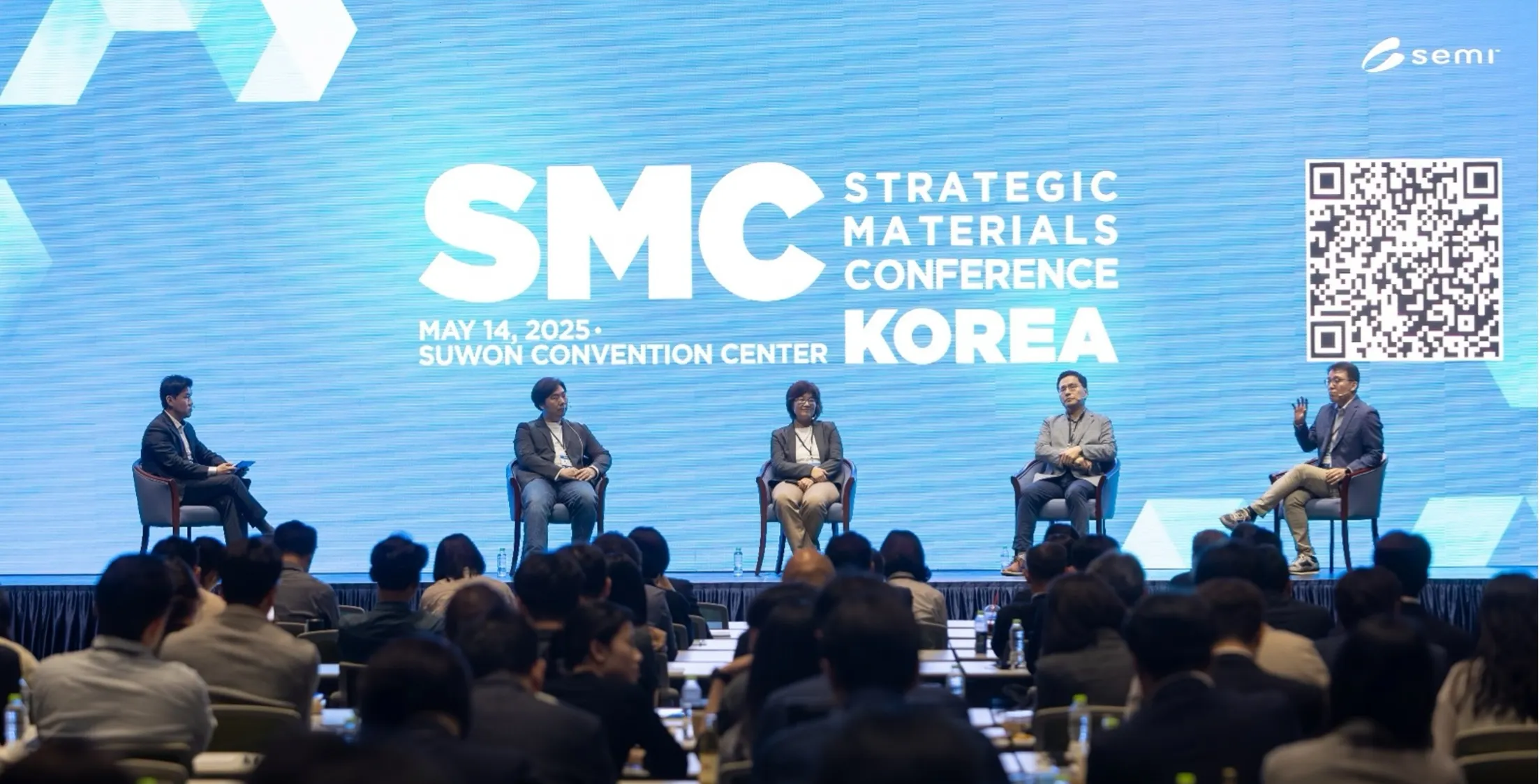
Panel Discussion
Networking Lunch
Emerging Etching Chemistry for Advanced Semiconductor Manufacturing
The rising technical demands for advanced semiconductor device manufacturing, and the industry’s ambitious net-zero commitments necessitate the development of novel etch chemistries that deliver both technical excellence and environmental sustainability. This talk will present an overview of the emerging etching chemistries developed by Air Liquide for variety-targeted applications. These innovative chemistries focus on delivering improved performance with unique technical merits to address current industry challenges. Exemplified by a novel low Global Warming Potential (GWP) designed for general dielectric etch, its synergistic integration with advanced abatement solutions, and a simplified Life Cycle Analysis (LCA) - from raw material extraction through processing, manufacturing, distribution, and use, this presentation aims to provide insights into a pathway towards more sustainable semiconductor manufacturing processes.

Enabling Advanced Metallization with Selective Deposition
As device architectures scale toward the angstrom era, metallization has emerged as one of the most critical bottlenecks to continued improvements in power and performance. Shrinking feature dimensions increase resistance, heighten reliability risks, and add complexity in interconnects and contacts. At these scales, traditional approaches which uniformly affect all wafer surfaces are increasingly ineffective. They rely heavily on lithography to define placement, and struggle to address tighter geometries and growing sensitivity to interfaces. Selective deposition is a solution which enables atomicscale control of where metals grow, placing material only where it is needed, without relying on patterning. It also enables monocrystalline metal growth, eliminating grain boundaries to minimize contact resistance.
This presentation will highlight how Applied Materials’ integrated materials solutions are enabling multiple inflections through area selective metallization. Selective Cobalt Capping technology encapsulates copper interconnects, improving adhesion, suppressing electromigration, and extending copper reliability to advanced nodes. Applied’s Selective Barrier eliminates a highly resistive interface at the interface of interconnect wiring. For contact fill, Applied developed Selective Tungsten (W) as a liner-less gap-fill solution that eliminates traditional liner/barrier layers and enables bottomup, seamfree metal fill. Finally, we introduce Selective Molybdenum (Mo) deposition that carries lowresistivity contact scaling forward as dimensions approach the fundamental scaling limits of W. Applied’s state-of-the-art atomic layer deposition tool for molybdenum delivers bottom-up, single-crystal Mo growth, enabling the next generation of contact scaling.
Next Generation Cleaning Processes and Materials
Cleaning processes originally relied on wet etch based patterning. However, dry etching now performs the majority of the patterning work, so wet etching is no longer needed for most pattern creation steps. Consequently, the focus of cleaning has shifted from patterning to the removal of contaminants. To obtain a clean surface, we must eliminate unwanted contaminants without any side effects such as pattern damage, collapse, material loss, or corrosion.
However, in the current era of 3 D structured devices such as V NAND, GAA, and 3 D DRAM, lateral wet etching is essential for patterning 3 D devices, and the proportion of wet etching in cleaning processes is increasing. Additionally, different kinds of selectivity such as concentration selectivity and area selectivity, have become important, in addition to conventional material selectivity. Sometimes we have to remove a film uniformly even though there are seams and voids. In addition, pattern loading has become a critical factor in lateral removal processes. We must solve these loading issues to achieve better performance and yield.
From time to time we must use more flexible, multi step processes; therefore, premixed chemistry is not enough to meet our purpose. Due to the flexibility of dry (gas phase) cleaning, the portion of dry cleaning has been increasing sharply. Area selectivity has also become another challenge. We must etch without corner rounding or climbing, and we want to perform anisotropic etching.
Conversely, based on the generic clean roadmap, high aspect ratio cleaning and low consumption cleaning will remain continuous challenges. Super critical CO2 drying is a solution for pattern collapse in HAR patterns, yet a dryer that is milder than CO2 but better than conventional IPA dryer technology is still required. In terms of chemical reduction, the puddle process may be a solution, but some side effects related to temperature consistency and cleanliness differences due to fluid dynamics must be resolved before implementation.
Networking Break
Panel Discussion
Adjourn
AI Enabled Materials Breakthroughs: From Molecules to Manufacturing
The transition toward an AI-driven technological landscape is redefining the paradigm of materials innovation across the semiconductor industry. In response, SMC (Strategic Materials Conference) Korea will spotlight next-generation semiconductor materials and process innovation strategies that enable and accelerate AI-driven advancements.
This conference brings together leading companies representing the global semiconductor ecosystem to share strategic directions and practical insights into materials innovation, from material design to real-world manufacturing processes.
The first session will focus on materials strategies for the AI era, exploring market and technology trends as well as AI-driven development approaches to provide a comprehensive view of next-generation semiconductor innovation. The second session will offer an in-depth exploration of process-ready materials essential for advanced semiconductor manufacturing, highlighting practical applications in areas such as photoresists, etching chemistry, and cleaning processes.
By convening key players across the semiconductor ecosystem, this conference provides a unique platform to gain a holistic perspective on the present and future of materials innovation in the AI era. Participants will have the opportunity to gain valuable technical insights while fostering collaboration and connections across the industry.