Off
Add to Calendar2026-02-11 00:00:002026-02-13 00:00:00SEMICON Korea 2026TRANSFORM TOMORROWThe future of the semiconductor industry starts here.Join us at SEMICON Korea 2026 to shape tomorrow together. HoursFebruary 11, 2026 | 10:00-17:00 (Last entry 16:30)February 12, 2026 | 10:00-17:00 (Last entry 16:30)February 13, 2026 | 10:00-16:00 (Last entry 15:30)VenueCOEX (Hall A, B, C, D, E, Grand Ballroom, Platz and ASEM Ballroom)Westin Seoul ParnasGrand InterContinental Seoul ParnasScale550 Exhibitors, 2409 booths (2025: 501 exhibitors, 2301 booths)Seoul South KoreaSEMI.org[email protected]America/Los_Angelespublic
Early-bird Registration Close: 3 pm, Friday, May 12(KST)
Registration Fee
Early Bird (~ May 12)
SEMI Member: KRW 280,000
Non Member: KRW 330,000
On site
SEMI Member/ Student : KRW 330,000
Non Member: KRW 380,000
※ Group registration fee applies if more than 5 people are registered from one company. Please contact us by email ([email protected] ) for group registration.
Convention Hall 2, Suwon Convention Center Suwon-si Gyeonggi-do South Korea
9:00 am
-
9:05 am
Welcome
Keynote
9:05 am
-
9:35 am
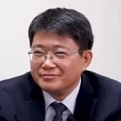
Namsung Kim
Senior Director
Applied Materials
GAA(Gate-All-Around) technology to enable continuous CMOS transistor scaling for energy efficient computing solution
Namsung Kim is a Senior Director in the Integrated Module Solutions (IMS) Group at Applied Materials. He is currently responsible for managing customer engagement programs, driving business growth, and leading cross-functional teams (various Business Units) to deliver the integrated materials/modules-base product solutions across leading-edge CMOS Logic and Memory technologies. Prior to this role, he has successfully led & accomplished the definition of CMOS Logic technology roadmap, its inflections of future technology nodes and delivered multiple product development paths by validating innovative pathway solutions.
He joined Applied Materials, Inc., USA in 2015, bringing over 20 years of semiconductor device/process integration experiences (various engineering/management positions) from both CMOS Logic (GlobalFoundries/IBM alliance in USA and SSMC in Singapore) and Memory (SK-Hynix, previously LG Semi., in Korea) industries. He earned a MS in electrical and computer engineering from the National University of Singapore. He has authored and co-authored more than 50 technical publications and holds over 40 patents in the field of advanced logic (FinFETs and GAA devices) and memory technologies.
Market & Technology Trends for Memory Devices including Materials
Dr. Jeongdong Choe is a Senior Technical Fellow at TechInsights. He has over 30 years of experience in the semiconductor industry, R&D, and reverse engineering on DRAM, NAND/NOR FLASH, SRAM/Logic, and Emerging Memory. He worked for SK Hynix and Samsung Electronics for over 20 years. He joined TechInsights and has been focusing on technology analysis of semiconductor processes, materials, devices, and architecture. He has written many articles on memory technology including roadmaps, technology trends, and detailed comparisons.
Session 1: Advanced Materials for Enabling Next-Generation Devices
10:50 am
-
11:15 am
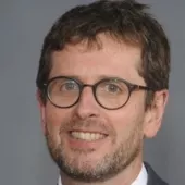
Jean-Marc Girard
CTO and Sr. VP
Air Liquide
Precursors for Memory
Jean-Marc Girard Ph.D. is CTO and Sr. VP of Manufacturing Technologies at Air Liquide Advanced Materials (ALAM), and an Air Liquid Group Fellow. He has 25 years of experience of R&D and product development management in the field of semiconductor materials and process technology in Europe, Japan and the US, and is one of the founders and was the global director of ALOHA™ from 2005 to 2010 (Air Liquide’s original CVD/ALD materials product line).
Within ALAM, Jean-Marc globally manages the Research and Development for deposition & advanced dry etching materials, oversees strategic engagements and collaborations with leading customers and equipment companies, and supervises the Intellectual Property generation and portfolio management. Since 2021, Jean-Marc’s role has expanded to leading packaging and manufacturing technology developments efforts.
11:15 am
-
11:40 am
Andy Kim
Sr. Director
Lam Research
Materials Trends in Semiconductor Manufacturing
“Byunghee Kim” has been Sr. Technologist in Lam Research since 2017.
Prior to joining Lam Research, “Kim” was director position for Samsung Electronics. During his 23 years at Samsung Electronics, “Kim” spent time doing module development, including gate, contact and BEOL.
“Kim” received a bachelor’s degree in chemistry from Yonsei Univ., Seoul, Korea and a master’s degree in MSE from Seoul Nat’l Univ., Seoul, Korea.
Jeongsik Kim, received a MS degree in Organic Synthetic Chemistry from Sogang University(Korean) in 2006 and then joined Dongjin Semichem. He had developed the patterning process materials such as bottom antireflective coating(BARC), spin on hardmask(SOH), photoresist materials in Semiconductor Materials Business Division since 2006. In 2013, he had joined the advanced lithography program of IMEC(Belgium) as Dongjin Semichem assignee and researched the ArF immersion patterning and defectivity for two years. Currently, he is in charge of developing EUV photoresist at Dongjin Semichem.
Sung Ho Kim is the Head of Specialty Gases Marketing, Clean & Etch platform, Merck KGaA, Darmstadt, Germany where he drives the execution of product marketing strategy to meet with industry’s dry etch and chamber clean gas technical and commercial needs, and leads product life cycle management and NPI (New product introduction) initiatives to help customers to advance its dry etch and chamber clean process performance. He is a proven business leader with more than 20 years of experience in the semiconductor materials industry, with a wide range of leadership experience in product marketing, product management, and technical/engineering expertise. He is based in Pangyo, Korea. Sung-Ho received a bachelor's degree in Chemical Engineering from Seoul National University.
Head of BASF Electronic Materials R&D Center in Suwon
BASF
Aiming CO2 neutrality – Sustainable Solutions for IC Applications
Won-Seob Cho, Ph.D. presently serves as the Head of the BASF Electronics Materials R&D Center in Suwon, Korea. In this esteemed position, he is responsible for leading research teams dedicated to the development of advanced wet chemical solutions, such as advanced cleaning and electroplating methods. He boasts over 20 years of research and development experience, particularly in the formulation and electrochemical screening of solutions.
Prior to joining BASF a decade ago, He served as a Principal Researcher at Samsung SDI and Samsung Fine Chemicals, where he specialized in developing planarization and electroplating solutions. Notably, his research interests have recently expanded to encompass the Advanced Package field.
Won-Seob Cho holds a distinguished Ph.D. in Chemistry from the University of Texas at Austin and has also served as a postdoctoral fellow in Supramolecular Chemistry at the University of California at Los Angeles, further solidifying his scientific expertise.
Carbon Neutral Strategy of Korean Government and Role of Material Companies
Dr. Nam, Sang Uk is conducting various studies on the ICT (semiconductor, display) industry based on economics at the KIET (Korea Institute of Industrial Research), a national research institute.
Since joining the KIET in 2018, he has participated in various studies on ICT industry policies such as Japanese export regulations, development strategy of material, parts and equipment, global value chain, and digital transformation.
In the field of carbon neutrality, he participated in major reports such as the semiconductor and display industry's carbon neutral promotion strategy and policy tasks, and the impact of RE100 on Korea's major export industries.
Materials still matter. Trends in materials demand and supply.
Mark Thirsk is Managing Partner of Linx Consulting, a leading management and strategic consulting company for electronic materials.
Mark Thirsk has experience spanning many materials and processes in wafer fabrication, combined with economic and business forecasting, strategic planning, technical marketing and M&A experience. Mark has worked in materials and equipment development, marketing, applications support, and production, as well as having expertise in business incubation, strategic development, and M&A. Mark is well placed to bring clarity and insight to market analysis from both a technical and commercial perspective. Additionally, Mark has been active in SEMI since 1999, volunteering in industry advocacy, education, and recruiting.
Mark has worked in the UK, Germany, Belgium, and the USA. Mark holds an Honours B.Sc. in Metallurgy and Materials Science from Birmingham University and an MBA
E. Jan Vardaman is president and founder of TechSearch International, Inc., which has provided market research and technology trend analysis in semiconductor packaging since 1987. She is the author of numerous publications on emerging trends in semiconductor packaging and assembly. She is a senior member of IEEE EPS and is an IEEE EPS Distinguished Lecturer. She received the IMAPS GBC Partnership award in 2012, the Daniel C. Hughes, Jr. Memorial Award in 2018, the Sidney J. Stein International Award in 2019, and she is an IMAPS Fellow. She is a member of MEPTEC, SMTA, and SEMI. Before founding TechSearch International, she served on the corporate staff of Microelectronics and Computer Technology Corporation (MCC), the electronics industry’s first pre-competitive research consortium.
Re-visioning Material Technology for Sustainable Resource Utilization and Supply Chain
Sam-Jong Choi, Ph.D. has been working as a material expert at Samsung Electronics Semiconductor for over 30 years. He joined the company in 1991 and has been responsible as a material engineer and expert for Memory Manufacturing Technology Center in Samsung Electronics by now. He obtained a Ph.D in Electronic, Computer, and Telecommunication Engineering from Hanyang University in 2020.
In 2019, he was promoted to Group Leader for Memory Material Technology Group, where he oversaw the development of new materials and quality management for Samsung Electronics. In 2020, Samjong Choi was appointed as an Corporate VP at Samsung Electronics, where he continues to play a key role in the field of semiconductor material.
As an experienced engineer and leader, he brings a wealth of knowledge and expertise to his current role, making Samsung Electronics stay at the forefront of technological innovation in the global semiconductor material industry.
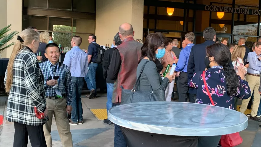
In the semiconductor industry, a stable and efficient global supply chain is as important as the continuous development of advanced technology. In addition to the trade conflict and reshoring, new trends such as GWP(Global Warming Potential) are highlighted, and prompt response of the Ecosystem is essential. Accordingly, SMC Korea is trying to provide an opportunity for the semiconductor industry to discuss issues that need to be spoken out together.
SMC Korea 2023 prepares various presentations to share information on the latest technologies and markets through the participation of global leading companies while also checking global warming potential (GWP) in terms of materials. Please join us in the insights of global experts!
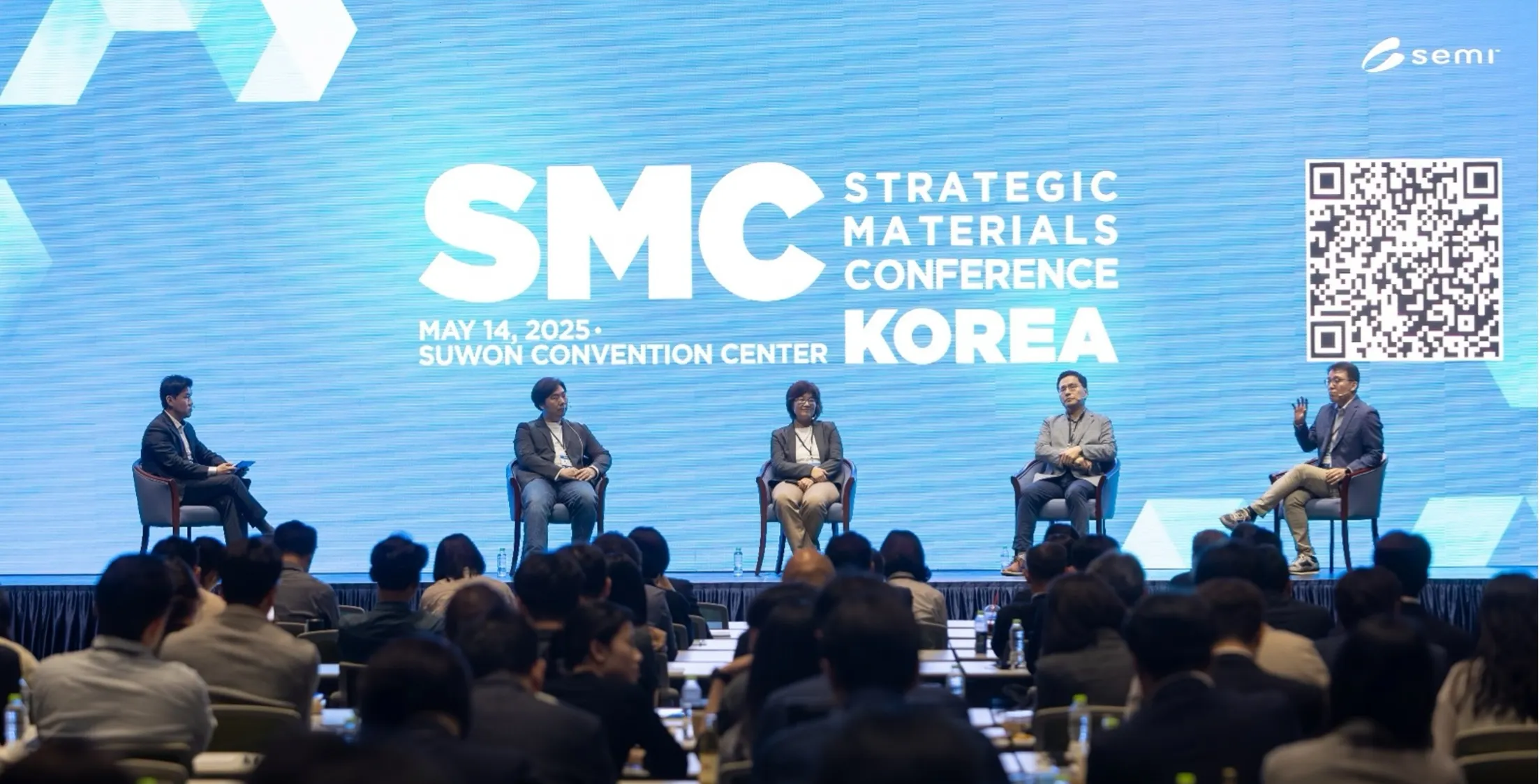
SMC (Strategic Materials Conference) Korea 2023
May 17(Wed), 2023 | Convention Hall 2, Suwon Convention Center
Off
Add to Calendar2023-05-17 00:00:002023-05-17 00:00:00SMC Korea 2023Semiconductor Materials for Sustainable Future
In the semiconductor industry, a stable and efficient global supply chain is as important as the continuous development of advanced technology. In addition to the trade conflict and reshoring, new trends such as GWP(Global Warming Potential) are highlighted, and prompt response of the Ecosystem is essential. Accordingly, SMC Korea is trying to provide an opportunity for the semiconductor industry to discuss issues that need to be spoken out together.
SMC Korea 2023 prepares various presentations to share information on the latest technologies and markets through the participation of global leading companies while also checking global warming potential (GWP) in terms of materials. Please join us in the insights of global experts!Convention Hall 2, Suwon Convention Center Suwon-si Gyeonggi-do South KoreaSEMI.org[email protected]Asia/Seoulpublic
Asia/Seoul
SMC3 - Register 3: 15% off (must register all 3 on same order)
SMC5 - Register 5: 20% off (must register all 5 on same order)
SMC10 - Register 10: 25% off (must register all 10 on same order)
NOTE: For Group Discounts, Attendees must be registered within the same order.
For more information, please contact Karen Popp, Senior Program Manager, at [email protected].
Registration is final. Cancellations will not be accepted. No refunds provided. Substitutions are only accepted with written permission from the original registrant.
Your health and safety are our top priority. The personal preference of the attendees to wear masks is respected at all SEMI events. SEMI Americas (“SEMI") monitors developing federal, state, and local health and safety recommendations as well as requirements regarding COVID to determine the most appropriate safety protocols for our in-person events.
Sponsorship opportunities can be tailored to meet your specific branding and marketing objectives. Become a sponsor and brand your company to an influential audience at SMC.
CONTACT
Shane Poblete Director, Sales & Business Development - Expo and Events, SEMI Tel: +1 202-847-5983 Email: [email protected]
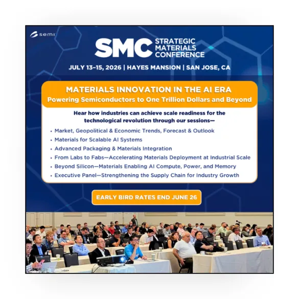
Materials Innovation in the AI Era: Powering Semiconductors to One Trillion Dollars and Beyond
Beyond the AI boom lies a challenge—and opportunity—that is far more foundational: ensuring the materials ecosystem underpinning a $2.5 trillion industry is resilient enough to support the next era of innovation. As artificial intelligence accelerates demand for advanced hardware, energy infrastructure, and high‑performance components, the pressure on global materials supply chains has never been greater.
This year, SMC explores how industries can achieve scale readiness through smarter design, diversified sourcing, sustainable processes, and breakthrough materials science. It invites leaders to look past the excitement of AI itself and toward the essential building blocks that will determine whether this technological revolution is secure and sustainable.
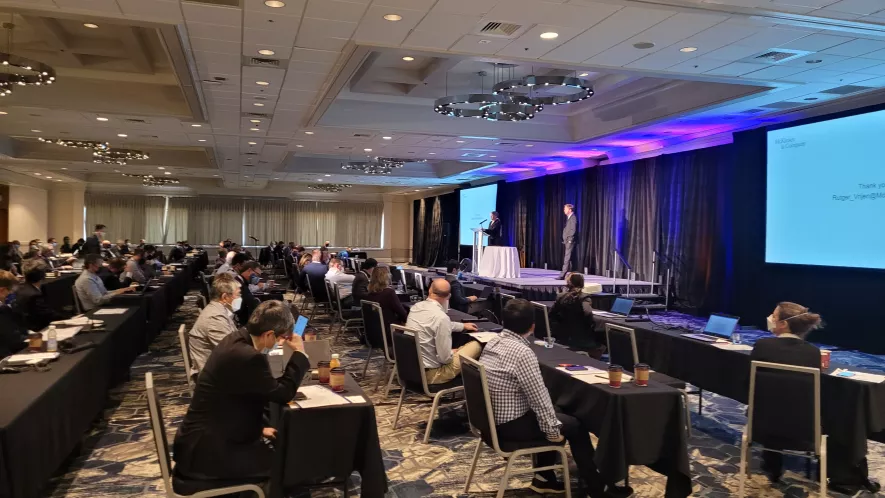
The Strategic Materials Conference—SMC offers valuable content and unprecedented networking opportunities for semiconductor industry professionals who share common strategic objectives on materials innovation, management, and business success.
Sessions
Market, Geopolitics & Outlook
Materials for Scalable AI Systems
Advanced Packaging & Materials Integration
From Labs to Fabs—Accelerating Materials Deployment at Industrial Scale
Quantum & Emerging Devices
Executive Panel–Strengthening the Supply Chain
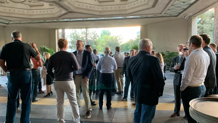
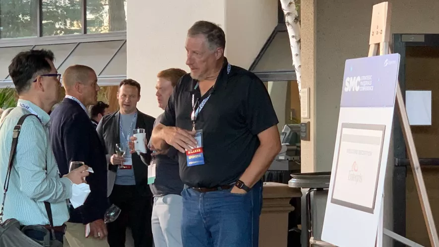
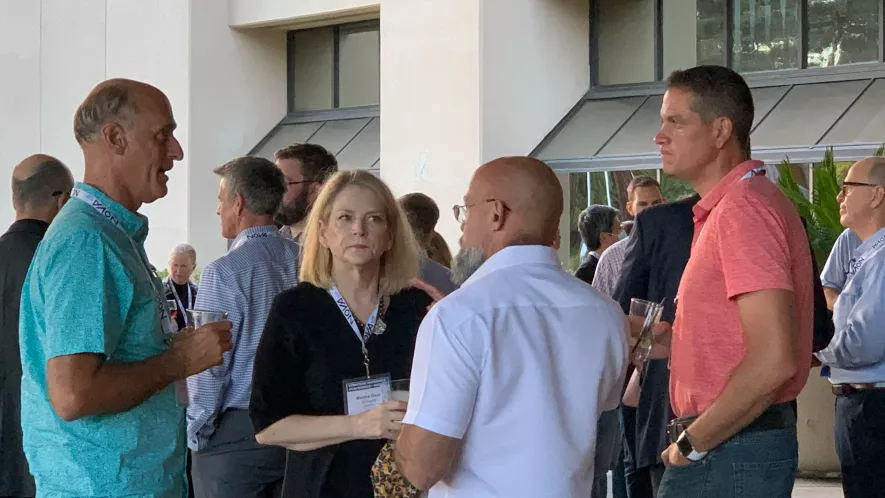
REGISTRATION INCLUDES
Approved speaker PDF presentations
Breakfast, lunch, coffee breaks
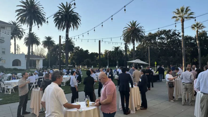
Two networking receptions
Tabletop exhibits
WHO SHOULD ATTEND
SMC offers valuable content and unprecedented networking opportunities for semiconductor industry professionals who share common strategic objectives on materials innovation, management, and business success.
CEO ● CTO ● Presidents & General Managers ● Executive VP & Senior Executives ● Engineering & Fab Managers ● Academia ● Startup Founders ● Financial Analysts ● Market Researchers ● Consulting Firms ● Consortiums
Off
Add to Calendar2026-07-13 00:00:002026-07-15 00:00:00SMC 2026—Strategic Materials Conference Hayes Mansion 200 Edenvale Avenue San Jose, CA, CA 95136 United StatesSEMI.org[email protected]America/Los_Angelespublic
America/Los_Angeles
1
Join the SEMI Water Management team and document authors for a webinar discussing their research and findings for the Water Management Strategy Reports. The reports are guides for water managers for understanding their water balance, baseline, potential savings and a general maturity scale for several solutions to be considered to move up the maturity scale to Zero Liquid Discharge (ZLD). The webinar will provide an overview on how the documents should be used to work with water solutions providers and provide strategies for both new and legacy facilities with end-of-pipe solutions as well as treatments for individual process stage water discharge.
The webinar will include a discussion of next steps for the continued development of the reports, including how they interact with SEMI Standards and the industry roadmaps.
9:00 am - 10:00 am
Off
Add to Calendar2026-05-21 09:00:002026-05-21 10:00:00Water Management Strategies WebinarJoin the SEMI Water Management team and document authors for a webinar discussing their research and findings for the Water Management Strategy Reports. The reports are guides for water managers for understanding their water balance, baseline, potential savings and a general maturity scale for several solutions to be considered to move up the maturity scale to Zero Liquid Discharge (ZLD). The webinar will provide an overview on how the documents should be used to work with water solutions providers and provide strategies for both new and legacy facilities with end-of-pipe solutions as well as treatments for individual process stage water discharge. The webinar will include a discussion of next steps for the continued development of the reports, including how they interact with SEMI Standards and the industry roadmaps.Reports can be downloaded HERE.United StatesSEMI.org[email protected]America/Los_Angelespublic
America/Los_Angeles
Register Here
Venue: Convention Hall 2, 3F, Suwon Convention Center
Language: Korean/English (Simultaneous interpretation will be provided)
NOTICE
The agenda is subject to change at the discretion of the speakers.
Presentation materials will be available for download after the conference via the SEMI Korea program registration website(https://semikrprogram.com), only for materials approved by the speakers for distribution.
VP, Advanced Technology Integration, Office of the CTO
Lam Research
How Wafer Processing Is Reshaping the 3D Era for AI
AI is fueling unprecedented growth and accelerating demand for advanced devices. Its requirements for performance, power, and area scaling are driving memory and logic devices toward 3D architectures.
At the heart of this 3D transformation, processing steps must enable taller, perpendicular structures as well as smaller features. Meeting these requirements calls for new deposition and etch capabilities that did not exist before, leading to breakthroughs needed in areas such as atomic-level deposition and etch (ALD and ALE), high-aspect-ratio processing, dry resist EUV patterning, and the adoption of new materials like molybdenum (Mo). As a result, the transition to 3D devices will drive increased intensity of deposition and etch processing.
This presentation will explore how deposition and etch are critical to unlocking the future of 3D devices, with increasing velocity required to meet the demands of AI-driven innovation.
Head of Technology & Innovation and President of Intermolecular®
Merck
Integrated Materials Innovation in the AI Era
As the semiconductor industry navigates the challenges of dimensional and functional scaling in the artificial intelligence (AI) era, advanced materials science has emerged as a critical enabler for performance enhancement. Modern AI-centric architectures demand the integration of increasingly complex system-on-chip (SoC) designs with non-traditional material systems.
This work details a high-throughput methodology for the rapid down-selection and optimization of multi-element thin films, ensuring alignment with both physical and electrical key performance indicators (KPIs). Utilizing combinatorial physical vapor deposition (PVD) in conjunction with unit-cell electrical test vehicles, we systematically screen an expansive elemental compositional space to identify optimal candidates. Advanced machine learning (ML) algorithms are integrated into each phase of the development lifecycle—spanning precursor synthesis, process optimization, and heterogeneous integration—to satisfy the rigorous specifications of emerging device applications. The synergy between integrated materials engineering and AI-driven informatics significantly reduces the temporal gap between material discovery and device-level implementation.
Chemical and materials research faces increasing demands for data-driven automation and autonomous research systems due to vast exploration spaces and complex decision-making processes. In this talk, we introduce EXAONE Discovery as a Chemical Agentic AI system and present an integrated research framework designed to accelerate scientific discovery.
EXAONE Discovery is an agent-based system that tightly integrates property prediction, molecular generation, synthesis prediction, and literature/data extraction. Based on given research objectives, the system accumulates relevant data, generates candidate molecules using model-driven approaches, evaluates their properties, and derives feasible synthetic routes—automating the end-to-end discovery pipeline. Furthermore, it is designed to enable a closed-loop research paradigm by interfacing with autonomous laboratories, connecting design–prediction–synthesis–validation cycles. This allows hypotheses proposed by AI to be experimentally validated, with results continuously fed back into the system for iterative model improvement and optimization.
In this talk, we will demonstrate how this integrated approach enhances research productivity across various industrial use cases in materials discovery and optimization, and discuss future directions of Chemical Agentic AI.
Emerging Etching Chemistry for Advanced Semiconductor Manufacturing
The rising technical demands for advanced semiconductor device manufacturing, and the industry’s ambitious net-zero commitments necessitate the development of novel etch chemistries that deliver both technical excellence and environmental sustainability. This talk will present an overview of the emerging etching chemistries developed by Air Liquide for variety-targeted applications. These innovative chemistries focus on delivering improved performance with unique technical merits to address current industry challenges. Exemplified by a novel low Global Warming Potential (GWP) designed for general dielectric etch, its synergistic integration with advanced abatement solutions, and a simplified Life Cycle Analysis (LCA) - from raw material extraction through processing, manufacturing, distribution, and use, this presentation aims to provide insights into a pathway towards more sustainable semiconductor manufacturing processes.
Enabling Advanced Metallization with Selective Deposition
As device architectures scale toward the angstrom era, metallization has emerged as one of the most critical bottlenecks to continued improvements in power and performance. Shrinking feature dimensions increase resistance, heighten reliability risks, and add complexity in interconnects and contacts. At these scales, traditional approaches which uniformly affect all wafer surfaces are increasingly ineffective. They rely heavily on lithography to define placement, and struggle to address tighter geometries and growing sensitivity to interfaces. Selective deposition is a solution which enables atomicscale control of where metals grow, placing material only where it is needed, without relying on patterning. It also enables monocrystalline metal growth, eliminating grain boundaries to minimize contact resistance.
This presentation will highlight how Applied Materials’ integrated materials solutions are enabling multiple inflections through area selective metallization. Selective Cobalt Capping technology encapsulates copper interconnects, improving adhesion, suppressing electromigration, and extending copper reliability to advanced nodes. Applied’s Selective Barrier eliminates a highly resistive interface at the interface of interconnect wiring. For contact fill, Applied developed Selective Tungsten (W) as a liner-less gap-fill solution that eliminates traditional liner/barrier layers and enables bottomup, seamfree metal fill. Finally, we introduce Selective Molybdenum (Mo) deposition that carries lowresistivity contact scaling forward as dimensions approach the fundamental scaling limits of W. Applied’s state-of-the-art atomic layer deposition tool for molybdenum delivers bottom-up, single-crystal Mo growth, enabling the next generation of contact scaling.
Cleaning processes originally relied on wet etch based patterning. However, dry etching now performs the majority of the patterning work, so wet etching is no longer needed for most pattern creation steps. Consequently, the focus of cleaning has shifted from patterning to the removal of contaminants. To obtain a clean surface, we must eliminate unwanted contaminants without any side effects such as pattern damage, collapse, material loss, or corrosion.
However, in the current era of 3 D structured devices such as V NAND, GAA, and 3 D DRAM, lateral wet etching is essential for patterning 3 D devices, and the proportion of wet etching in cleaning processes is increasing. Additionally, different kinds of selectivity such as concentration selectivity and area selectivity, have become important, in addition to conventional material selectivity. Sometimes we have to remove a film uniformly even though there are seams and voids. In addition, pattern loading has become a critical factor in lateral removal processes. We must solve these loading issues to achieve better performance and yield.
From time to time we must use more flexible, multi step processes; therefore, premixed chemistry is not enough to meet our purpose. Due to the flexibility of dry (gas phase) cleaning, the portion of dry cleaning has been increasing sharply. Area selectivity has also become another challenge. We must etch without corner rounding or climbing, and we want to perform anisotropic etching.
Conversely, based on the generic clean roadmap, high aspect ratio cleaning and low consumption cleaning will remain continuous challenges. Super critical CO2 drying is a solution for pattern collapse in HAR patterns, yet a dryer that is milder than CO2 but better than conventional IPA dryer technology is still required. In terms of chemical reduction, the puddle process may be a solution, but some side effects related to temperature consistency and cleanliness differences due to fluid dynamics must be resolved before implementation.
AI Enabled Materials Breakthroughs: From Molecules to Manufacturing
The transition toward an AI-driven technological landscape is redefining the paradigm of materials innovation across the semiconductor industry. In response, SMC (Strategic Materials Conference) Korea will spotlight next-generation semiconductor materials and process innovation strategies that enable and accelerate AI-driven advancements.
This conference brings together leading companies representing the global semiconductor ecosystem to share strategic directions and practical insights into materials innovation, from material design to real-world manufacturing processes.
The first session will focus on materials strategies for the AI era, exploring market and technology trends as well as AI-driven development approaches to provide a comprehensive view of next-generation semiconductor innovation. The second session will offer an in-depth exploration of process-ready materials essential for advanced semiconductor manufacturing, highlighting practical applications in areas such as photoresists, etching chemistry, and cleaning processes.
By convening key players across the semiconductor ecosystem, this conference provides a unique platform to gain a holistic perspective on the present and future of materials innovation in the AI era. Participants will have the opportunity to gain valuable technical insights while fostering collaboration and connections across the industry.
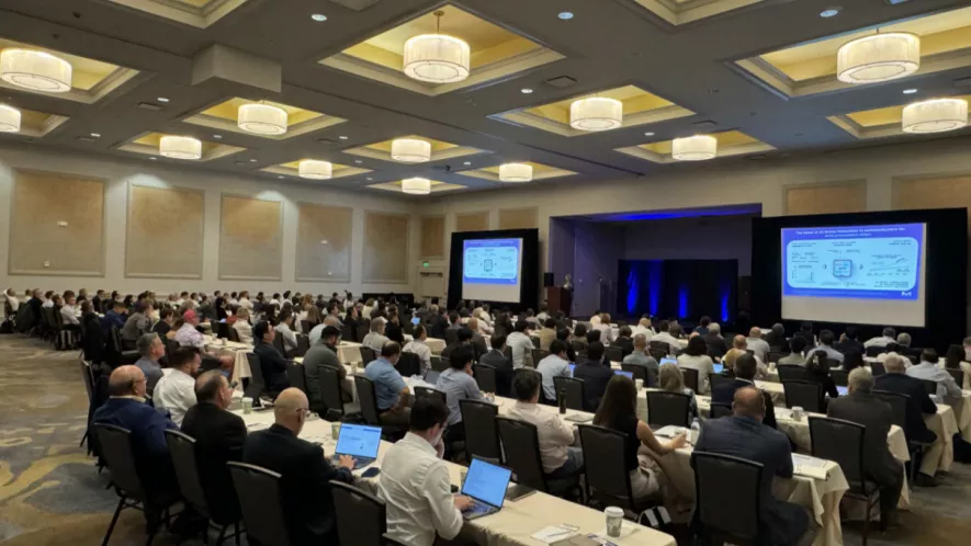
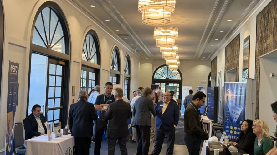
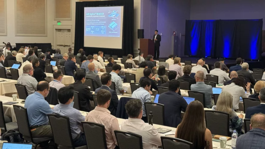
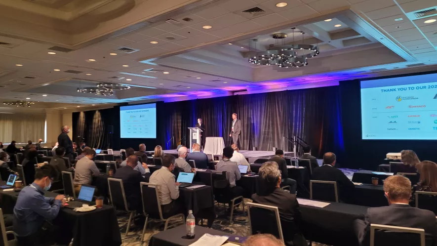
SMC (Strategic Materials Conference) Korea 2026
May 12(Tue), 2026 | Convention Hall 2, 3F, Suwon Convention Center
8:30 am - 4:30 pm
Off
Add to Calendar2026-05-12 08:30:002026-05-12 16:30:00SMC (Strategic Materials Conference) Korea 2026AI Enabled Materials Breakthroughs: From Molecules to ManufacturingThe transition toward an AI-driven technological landscape is redefining the paradigm of materials innovation across the semiconductor industry. In response, SMC (Strategic Materials Conference) Korea will spotlight next-generation semiconductor materials and process innovation strategies that enable and accelerate AI-driven advancements. This conference brings together leading companies representing the global semiconductor ecosystem to share strategic directions and practical insights into materials innovation, from material design to real-world manufacturing processes. The first session will focus on materials strategies for the AI era, exploring market and technology trends as well as AI-driven development approaches to provide a comprehensive view of next-generation semiconductor innovation. The second session will offer an in-depth exploration of process-ready materials essential for advanced semiconductor manufacturing, highlighting practical applications in areas such as photoresists, etching chemistry, and cleaning processes. By convening key players across the semiconductor ecosystem, this conference provides a unique platform to gain a holistic perspective on the present and future of materials innovation in the AI era. Participants will have the opportunity to gain valuable technical insights while fostering collaboration and connections across the industry.Suwon Convention Center South KoreaSEMI.org[email protected]Asia/Seoulpublic
Asia/Seoul
Are We There Yet? Metrology and Inspection for Angstrom-Level Manufacturing
In the semiconductor industry where we routinely pattern sub-wavelength structures and require atomic-layer precision in our manufacturing processes, it’s easy to assume that we can simply measure everything we’re doing and all the structures we create. In reality, though, metrology and inspection have the challenging task of not just keeping up with device technology but staying far enough ahead that we can actually “see” our results and confirm the progress we’re making.
In this webinar, co-hosted with the Electronics business of Merck KGaA, Darmstadt, Germany; we will explore the metrology and inspection space to learn more about technological advances driving this vital segment of semiconductor manufacturing.
The webinar will feature presentations by Eric Beyne, PhD, Senior Fellow, VP R&D and Director of 3D System Integration Program for imec, and Dario Alliata, PhD, Senior Application Director for Metrology & Inspection at the Electronics business of Merck KGaA, Darmstadt, Germany.
Following the presentations, an interactive Q&A segment will allow attendees a chance to deepen their understanding of how materials innovation and advanced metrology intersect at the leading edge of manufacturing.
Join us to engage with peers and pioneers working at the forefront of materials science and semiconductor innovation!
United States
Dario Alliata, PhD
Senior Director of Applications
The Electronics business of Merck KGaA, Darmstadt, Germany
The Role & the Challenge of Metrology and Inspection in Advanced Packaging of AI Chips
The massive adoption of social networking and artificial intelligence has pushed the semiconductor industry to develop devices capable of supporting the required infrastructures. Increasingly powerful computer process units (CPU) are used to allow data centers to process trillions of information exchanges, while faster graphic process units (GPU) enable virtual and assisted reality.
Cost leveraging is now reachable with the integration of multiple dies in the same package, each one fabricated to handle specific functionalities with the most cost-effective technology node, which is a form of heterogeneous integration. This session highlights some examples of metrology and inspection solutions aimed at securing the manufacturability of devices for High Computing Power fundamental for AI applications. More in detail, it explores the challenge of the fabrication of chip-to-chip interconnections that are key for the heterogeneous integration of active components with vertical stacking like DRAM for High Bandwidth memories, where process tolerances are increasingly narrow and conditions to measure more and more extremes.
Biography
Dr. Dario Alliata joined Unity-SC, now part of the Electronics business of Merck KGaA, Darmstadt, Germany in the U.S. and Canada. In 2016 as product manager and is now Sr. Director of Applications with focus on Advanced packaging and Specialty substrates & devices.
He worked in the semiconductor industry for more than 25 years, initially in R&D centers and later in equipment makers. He spent his entire career developing process control solutions for securing the manufacturing chain in the semiconductor industry.
He received a MD in Physics from the University of Milan (Italy) and hold a Ph.D. in Physics & Chemistry from the University of Berne (Switzerland).
Eric Beyne, PhD
VP R&D / Program Director 3D System Integration Program / Senior Fellow
imec
Sub-Micron Pitch Scaling of Hybrid Bond Interconnects: Metrology Challenges
Advanced 3D integration technology will increasingly rely on hybrid bonding technology for both wafer-to-wafer and die-to-wafer bonding. This allows for micrometer and sub-micrometer pitch interconnects, resulting in very high 3D interconnect densities, compatible with the back-end-of -line interconnect layers of active logic and memory die. The results are “seamlessly” interconnected die. Off-chip interconnects become equivalent (or better) than on-chip interconnects.
These great system-level benefits however come at some challenges. Small overlay errors or surface imperfections can prevent defects, resulting in yield loss. Critical process, steps, such as CMP, wafer dicing and surface cleaning steps, need to be monitored with higher accuracy to maintain a good process. New parameters, such as wafer shape, distortion, surface profile slopes, and copper pad recess levels need to be measured and continuously monitored. This poses significant challenges to metrology related to hybrid bonding. The presentation will highlight these needs and show some practical solutions.
Biography
Eric Beyne obtained a degree in electrical engineering in 1983 and the Ph.D. in Applied Sciences in 1990, both from the Katholieke Universiteit Leuven, Belgium. Since 1986 he has been with IMEC in Leuven, Belgium where he has worked on advanced packaging and interconnect technologies. Currently, he is imec senior fellow, VP R&D and program director of imec’s 3D System Integration program.
Michael Weigand
Senior Application Manager
Brewer Science
Moderator
Biography
I'm a seasoned Senior Application Manager at Brewer Science with over two decades of experience in Semiconductor industry. I lead application teams at Brewer Science Inc, focusing on advanced materials for the semiconductor industry. With a background in Material Science, I enjoy tackling technical challenges, from optimizing critical processes to finding creative ways to characterize materials.
Sponsored by the Electronics business of Merck KGaA, Darmstadt, Germany
Are We There Yet? Metrology and Inspection for Angstrom-Level Manufacturing
10:00 am - 11:00 am
Off
Add to Calendar2025-09-17 10:00:002025-09-17 11:00:00Are We There Yet? Metrology and Inspection for Angstrom-Level Manufacturing Sponsored by the Electronics business of Merck KGaA, Darmstadt, Germany United StatesSEMI.org[email protected]America/Los_Angelespublic
America/Los_Angeles
WATCH NOW