downloadGroupGroupnoun_press release_995423_000000 copyGroupnoun_Feed_96767_000000Group 19noun_pictures_1817522_000000Member company iconResource item iconStore item iconGroup 19Group 19noun_Photo_2085192_000000 Copynoun_presentation_2096081_000000Group 19Group Copy 7noun_webinar_692730_000000Path
Skip to main content
Default Banner Image

Virtual

If you are an employer wanting to get involved, please contact: 

Melinda Gomez 

mgomez@semiorg

+
United States [email protected]
Highlighted content

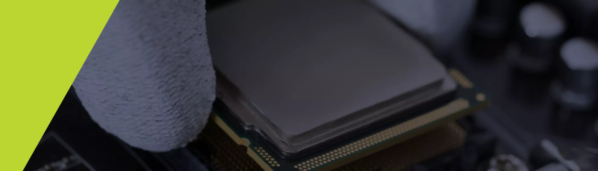
This webinar will introduce members of the military community to the semiconductor industry and connect them directly with veterans and recruiters. Employers recognize and need this skilled and talented community to join as the industry prepares for huge growth in the next few years.  We will dive into the roles expected and qualifications needed to jump into an exciting new career. Opportunities nationwide!


About SEMI VetWorks


The SEMI VetWorks Initiative aims to address the microelectronics industry's need for attracting, developing, and retaining talent by tapping into the skills and experiences of military veterans and reservists. SEMI prioritizes connecting its members with this talented pool through initiatives that align industry hiring practices, internship, and apprenticeship programs. By leveraging existing training and credentialing opportunities, veterans gain access to well-paid technician and operator roles. The SEMI VetWorks Guidebook offers tools and recommendations for recruiting, hiring, and retaining veterans, while the SHRM Veterans at Work Certificate program provides additional resources for connecting with the military community.

United States

9:00 am - 9:30 am
Melinda Headshot Round
Melinda Gomez
Program Manager, Veteran Initiatives
SEMI Foundation

Industry Overview and Trends

9:30 am - 10:00 am

Panel of Veterans in the Industry

10:00 am - 10:30 am

Panel of Industry Needs

10:30 am - 11:00 am

Breakout rooms to network with employers

Workforce Development

Members of the Military Community, join us for an interactive and informative session about career opportunities in the semiconductor industry. Hear from employers and veterans in the industry directly!

9:00 am - 11:00 am Off Add to Calendar 2024-03-26 09:00:00 2024-03-26 11:00:00 SEMI VetWorks: Careers in Chips Members of the Military Community, join us for an interactive and informative session about career opportunities in the semiconductor industry. Hear from employers and veterans in the industry directly! United States SEMI.org [email protected] America/Los_Angeles public America/Los_Angeles Watch On-demand
Event format
United States Spectrochip tile Business Technical Featured Speakers

Kevin (Cheng-Hao) Ko received his Physics Ph.D. from State University of New York, Stony Brook (SUNY, Stony Brook) in 1995. During his thesis research, he worked at Beamline X1A of the National Synchrotron Light Source (NSLS) at Brookhaven National Laboratory (BNL) to construct the world's first Mult-channel Scanning Photoemission Electron Microscope (SPEM) by focusing soft X-rays using a zone plate under the supervision of Prof. Janos Kirz. After receiving his Ph.D. degree, he was invited by Taiwan Nation Synchrotron Radiation Research Center (NSRRC) to lead a team to develop X-ray Microcopy technology in Taiwan. By 1999 Ko’s team had successfully developed the world’s most advanced SPEM. After that, Dr. Ko started to devote his efforts to developing the SpectroChip technology. After nearly 20 years of research and development, Ko’s team was finally able to mass produce the SpectroChip using wafer-based methodology and founded the company SpectroChip, Inc. This technology received 9 national best innovation awards in Taiwan and one international best application award in Asia. To enable further global business development of the SpectoChip technology, in 2023, Dr. Ko and Dr. Sean Lin founded SPU System Inc.

United States

dr. ko
Dr. Kevin (Cheng-Hao) Ko
MSIG

SpectroChip is a breakthrough technology that integrates all the functions of an optical spectrometer on a chip with the size of half an SD card.  It is designed and fabricated using X-ray lithography and microelectromechanical systems (MEMS) technology.  The current chip module includes the slit, micro concave grating and mirror and has a spectral range from 300 to 1000 nm. SpectroChip technology has the advantage of high performance with high sensitivity and accuracy while achieving chip-size miniaturization.  This technology is being applied to the development of ultra-compact optical sensors and/or devices that can deliver real-time spectral data and analysis. Examples include novel optical sensor modules and ultra-compact, high-performance spectrophotometers capable of UV/VIS and florescence analysis for research lab and educational purposes.

In this webinar Dr. Ko will describe the SpectroChip technology, its integration into optical spectrum processing units, and real-world sensing applications in Health Care, Food Safety, and Semiconductor Processing and Metrology.

8:00 am - 9:00 am Off Add to Calendar 2024-02-21 08:00:00 2024-02-21 09:00:00 SpectroChip: an Optical System-on-Chip Enabling Ultra-Portable Devices for Broad Industrial Sensing Applications SpectroChip is a breakthrough technology that integrates all the functions of an optical spectrometer on a chip with the size of half an SD card.  It is designed and fabricated using X-ray lithography and microelectromechanical systems (MEMS) technology.  The current chip module includes the slit, micro concave grating and mirror and has a spectral range from 300 to 1000 nm. SpectroChip technology has the advantage of high performance with high sensitivity and accuracy while achieving chip-size miniaturization.  This technology is being applied to the development of ultra-compact optical sensors and/or devices that can deliver real-time spectral data and analysis. Examples include novel optical sensor modules and ultra-compact, high-performance spectrophotometers capable of UV/VIS and florescence analysis for research lab and educational purposes.In this webinar Dr. Ko will describe the SpectroChip technology, its integration into optical spectrum processing units, and real-world sensing applications in Health Care, Food Safety, and Semiconductor Processing and Metrology. United States SEMI.org [email protected] America/Los_Angeles public America/Los_Angeles Watch On-demand
Event format
CAST logo

About Collaborative Alliance of Semiconductor Test (CAST)

CAST serves SEMI members and other stakeholders in the semiconductor test area. CAST members include leaders from automated test equipment (ATE) companies, fabless, IDMs, and OSAT companies. CAST members work with their customers, suppliers, and industry colleagues to develop industry standards that reduce costs and spur innovation.

CAST logo
United States 453x388_Homepage_Ad_tile_Spectro_3.png Technical
Highlighted content

Unlike the semiconductor ‘frontend’, the ‘backend’ has little standardization with lots of different interfaces and behaviors between different equipment suppliers.  How can we standardize it and gain the efficiencies that standards brought to the frontend?  SEMI has several standards suites that could be used depending on the customer’s needs, including SECS/GEM, EDA/Interface A and RITdb.  This webinar will describe the benefits of each, as well discuss challenges around traceability and other issues commonly encountered in the backend, and how standards can benefit the equipment users.

United States

3:00 pm - 3:05 pm
Alan Weber
Vice President, New Product Innovations
Cimetrix

Opening Remarks

Alan Weber is currently the Vice President, New Product Innovations for Cimetrix Incorporated. Previously he served on the Board of Directors for eight years before joining the company as a full-time employee in 2011.

Alan has been a part of the semiconductor and manufacturing automation industries for over 40 years. He holds bachelor's and master's degrees in Electrical Engineering from Rice University.

3:05 pm - 3:15 pm
Brian Rubow
Director of Solutions Engineering
Cimetrix

SECS/GEM

Brian Rubow is the Director of Solutions Engineering for Cimetrix. He is well-known within the industry due to his involvement with the SEMI standards committees. He currently serves as the co-chairs for the North America Information and Control Committee, the North America GEM300 Task Force, and the North America DDA Task Force. Rubow has both a bachelor’s and a master’s in engineering from Brigham Young University.

3:15 pm - 3:25 pm
Albert Fuchigami
Senior Software Developer
PEER Group

EDA/Interface A

Albert Fuchigami is a senior software developer at PEER Group Inc. and has spent more than 20 years helping semiconductor OEMs integrate their equipment into factories around the world. He is a globally recognized leader in the SEMI Standards Program, co-leads the North America Data Diagnostic Acquisition (DDA) Task Force, and contributes to the Information & Control Technical Committee. Albert enjoys demonstrating how standards can maximize data communication with factory host systems and is a champion for integrating HTTP/2 with gRPC and Protocol Buffers technology into the Equipment Data Acquisition (EDA) / Interface A standards. He holds a Bachelor of Mathematics (Computer Science) degree from the University of Waterloo.

3:25 pm - 3:35 pm
Stacy Ajouri
Senior Member of Technical
Texas Instruments
Mark Roos
CEO
Roos Instruments

RITdB

Stacy Ajouri is a Senior Member of Technical Staff at Texas Instruments in the Test Technology Group. She is the co-chair of the North America Automated Test Equipment (ATE) Technical Committee and the RITdb Task Force. She has over 30 years of experience across multiple disciplines related to test and test operations. Pulling from that experience, she supports the implementation of RITdb proof of concepts (POCs) focusing what is needed by the manufacturing and engineering community.

Mark Roos is CEO of Roos Instruments, a longtime producer of semiconductor ATE. He co-chairs the North America ATE Technical Committee and the RITdb Task Force. Roos has been involved in standards development for ATE for the past 20 years. He is currently heavily involved in the focus of RITdb POCs on scaling and latency.

3:35 pm - 3:45 pm
Dave Huntley
Product Manager Assembly Products
PDF Solutions

Traceability and E142

Dave Huntley was the founder and president of KINESYS Software in 1992 which developed the Assembly Line Production Supervisor (ALPS). PDF Solutions acquired the ALPS in 2017 and Dave now works in Strategic Marketing, Business Development & Standards Liaison focused on defect / process tracking and single device traceability across the supply chain.

He has a long history working with SEMI. He was co-lead of the Sort Map task force responsible for the SEMI E142 Specification for Substrate Mapping Standard. Dave is now the co-lead for the Traceability committee and two SEMI task forces; 1) Advanced Backend Factory Integration working on applying and extending wafer fab automation standards to assembly and test and 2) Single Device Traceability task force working on blockchain traceability for the supply chain.

3:45 pm - 3:55 pm
Alan Weber
Vice President, New Product Innovations
Cimetrix

Closing Remarks

CAST 3:00 pm - 4:00 pm Off Add to Calendar 2024-02-22 15:00:00 2024-02-22 16:00:00 Standardizing the Semiconductor Manufacturing Backend United States SEMI.org [email protected] America/Los_Angeles public America/Los_Angeles

CAST logo

About Collaborative Alliance of Semiconductor Test (CAST)

CAST serves SEMI members and other stakeholders in the semiconductor test area. CAST members include leaders from automated test equipment (ATE) companies, fabless, IDMs, and OSAT companies. CAST members work with their customers, suppliers, and industry colleagues to develop industry standards that reduce costs and spur innovation.

Watch On-demand
Event format

Registration

Member Price: $49

Non-Member Price: $99

Registration is final. No refunds provided. No substitutions.

Krish Raghunath
Email: [email protected]
Phone: +1.408.943.6982

+
United States Semiconductor Industry Outlook Thumbnail Business Executive
Taiyo Nippon Sanso
Vaisala Logo 170x65

Become a Sponsor

Sponsorships can be tailored to meet your branding and marketing objectives. Become a sponsor and brand your company at the Silicon Valley & Northeast Virtual Forum.

Contact Tim Janes, [email protected] to learn about available sponsorship opportunities.

The SEMI Silicon Valley and Northeast Chapters Present:

Semiconductor Industry Outlook 2026 

As we step into 2026, the semiconductor industry continues to evolve at an unprecedented pace, driven by technological innovation, global market dynamics, and shifting economic conditions. Join us for an engaging virtual forum where leading experts will share insights into the trends, challenges, and opportunities shaping the future of the semiconductor ecosystem.

Topics Include:

  • Key market and technology trends shaping the industry.
  • Expert forecasts for 2026 and beyond.
  • Geopolitical impacts.
  • Emerging and expanding markets

Don’t miss out—register now to secure your spot!
 

United States

Virtual Forum | Wednesday, March 4, 2026 | Pacific Time

8:30 am
Joe Stockunas
Joe Stockunas
President
SEMI Americas

Welcome Remarks

8:35 am
Luke Chang
Moderator
Luke Chang, PhD
Silicon Valley Chair; Program Director
SCREEN

Welcome Remarks

8:40 am
Duncan Meldrum, Headshot
Duncan Meldrum, PhD, CBE™
Business Economist
Hilltop Economics

Uncertainty and the Economic Outlook - Economic Growth and Semiconductors: Focus on the Risks

9:05 am
Scarlett Bickerton
Scarlett Bickerton
Manager, Federal & State Affairs
SEMI

SEMI Advocacy: Shaping the Policy Impacting Corporate Initiatives

9:30 am
Rebecca Routson
Rebecca Routson
Principal Director
CHIPS Metrology Program

CHIPS Metrology Program Update

9:55 am
Joe Gaustad, ClassOne
Joe Gaustad
Director of Product Development
ClassOne Technology

The New 300mm Customer

10:20 am
 Inna Skvortsova
Inna Skvortsova
Research Manager, Market Intelligence
SEMI

From AI Gold Rush to Fab Reality: Capacity, Fab Investments and Materials Outlook

10:45 am

Q&A

10:55 am
Sophia Rogalskyj_TEL
Sophia Rogalskyj
Etch Development Engineer and Northeast Chapter Co-Chair
NY Creates

Closing Remarks

8:30 am - 11:00 am Off Add to Calendar Disabled America/Los_Angeles 2 Register Now
Event format
Promote in calendar
Off

REGISTRATION

Registration is free.

Belgium France Germany Ireland Italy Japan South Korea United States REGISTER NOW EPA Thumbnail Image_NEW Business Executive

The webinar will feature senior leaders and other experts from EPA and provide SEMI members with an overview of EPA’s efforts under the PFAS Strategic Roadmap; the recently finalized reporting rules under the Toxic Substances Control Act (TSCA) and the Toxics Release Inventory (TRI) program; the review and management of new PFAS chemicals under the TSCA New Chemicals program; and an update on research and development activities, including analytical test methods development.  In addition to hearing directly from EPA officials on these important topics, participants will have an opportunity to ask questions at the end.  

United States

Welcome Remarks

1:00 pm
Joe Stockunas, SEMI Americas
Joe Stockunas
President
SEMI Americas

Speakers

Michal Freedhoff, PhD, U.S. Environmental Protection Agency
Dr. Michal Freedhoff
Assistant Administrator, Office of Chemical Safety and Pollution Prevention
U.S. Environmental Protection Agency
Matt Klasen, U.S. Environmental Protection Agency
Matt Klasen
PFAS Council Manager
U.S. Environmental Protection Agency
Susan Burden, PhD, U.S. Environmental Protection Agency
Dr. Susan Burden
PFAS Executive Lead, Office of Research and Development
U.S. Environmental Protection Agency
Stephanie Griffin, U.S. Environmental Protection Agency
Stephanie Griffin
Team Lead, Data Collection Branch, Office of Pollution Prevention and Toxics
U.S. Environmental Protection Agency
Shari Barash, U.S. Environmental Protection Agency
Shari Barash
Acting Director, New Chemicals Division, Office of Pollution Prevention and Toxics
U.S. Environmental Protection Agency
Tyler Lloyd, U.S. Environmental Protection Agency.jpg
Tyler Lloyd
Team Leader, Risk Management Branch 1, New Chemicals Division, Office of Pollution Prevention and Toxics
U.S. Environmental Protection Agency
2:00 pm

Adjourn

Join us to learn more about several of the U.S. Environmental Protection Agency’s recent actions related to PFAS and their relevance to the semiconductor manufacturing industry.

1:00 pm - 2:00 pm Off Add to Calendar Disabled America/New_York
Event format

Registration is free

Belgium France Germany Ireland Italy Japan South Korea United States ESDA_Thumbnail Image Business Executive
Highlighted content

United States

Moderator

9:00 am
Raj Gautam Dutta, CEO, Silicon Assurance
Moderator
Raj Gautam Dutta
CEO
Silicon Assurance

Panelists

Serge Leef
Serge Leef
Head of Secure Microelectronics
Microsoft
Swarup Bhunia, Semmoto Endowed Professor and Director of Warren B. Nelms Institute
Swarup Bhunia
Semmoto Endowed Professor and Director
Warren B. Nelms Institute
Salman Nasir
Salman Nasir
Sr. Technical Program Manager
Battelle
John Hallman
John Hallman
Digital Verification Technology Solutions Manager
Siemens EDA
Steve Carlson
Steve Carlson
Director/Solutions Architect, Aerospace and Defense Solutions
Cadence Design Systems
Ming Zhang
MIng Zhang
VP of R&D Acceleration
PDF Solutions
EMG

Many semiconductor-based systems are moving toward 2.5D and 3D designs consisting of different pre-manufactured chips (chiplets) that perform specific functions. These are often provided by multiple vendors and are typically interconnected using an interposer. However, unlike monolithic multi-function chips, chiplets can be developed anywhere and at any process node. As such, chiplets from untrusted vendors can be unreliable or malicious. Third parties can reverse engineer, overproduce, or steal the IP of chiplets. Consequently, they raise new security challenges for an industry still figuring out ways to effectively mitigate hardware security threats to monolithic chips.

The webinar will focus on the potential threats that occur at the different stages of bringing chiplets to life, including design, assembly, and testing. The panelists will assess current safeguards to mitigate these risks and discuss open challenges for industry and academia.

9:00 am - 10:00 am Off Add to Calendar Disabled America/Los_Angeles Register Now
Event format

Registration for this course is free.

For questions, please contact Paul Trio at [email protected]

+
Belgium China France Germany India Ireland Italy Japan Malaysia Russia Singapore South Korea Taiwan United States Vietnam EMS course Ad tile Business Executive

Electromagnetic Interference and Electrical Overstress Management: Why, What, and How

Electromagnetic interference (EMI) is becoming more critical in all aspects of semiconductor manufacturing, affecting productivity and yield.  

The SEMI E176 Standard, "Guide to Assess and Minimize Electromagnetic Interference (EMI) in a Semiconductor Manufacturing Environment," addresses this issue. This document provides practical, actionable guidance on establishing an acceptable EMI environment in semiconductor processes: from assessing the EMI environment to EMI mitigation to verification. SEMI E176 sets recommended EMI limits for different process categories. The Standard can benefit every stage of the semiconductor process and electronic assembly.  
 

Who Should Attend:

  • Semiconductor Device Manufacturers
    • Manufacturing and Quality Directors
    • Department and Production Managers
    • Line Supervisors
    • Sales: VP and Managers
  • Equipment Manufacturers
    • Director-Level and VP Engineering and QA
    • Engineering Department Managers
    • Sales: VP and Managers (customer satisfaction)


Meet the Instructor

Vladimir Kraz


Vladimir Kraz, President, OnFILTER

Biography


SEMI HQ
CA
United States

1. Overview of SEMI and SEMI Standards
- SEMI as a resource for your company

2. EMI and EMC - an overview

3. Effect of EMI on processes and equipment
- EMI and Electrical Overstress
- Equipment precision
- Process variations
- Other problems

4. Sources and propagation of EMI

5. Overview of SEMI E.33
- Emphasis on Table 1: Compliance Assignment/Responsibility Table

6. Overview of SEMI E.176

7. Basics of a viable EMI program at a factory based on SEMI E.176
- Purpose
- Structure
- Resources and budget
- Similarity and synergy with already-existing ESD program

Standards

Join us for a hybrid experience with both in-person and virtual attendance options.

4:00 pm - 5:00 pm Off Add to Calendar 2023-12-18 16:00:00 2023-12-18 17:00:00 EMI and EOS Management Course Join us for a hybrid experience with both in-person and virtual attendance options. SEMI HQ CA United States SEMI.org [email protected] America/Los_Angeles public America/Los_Angeles Register now
Event format

Registration

Registration is free 

United States Leveraging the CHIPS Act Thumbnail Business Executive

Leveraging the CHIPS Act in the Silicon Heartland: Ohio Semiconductor Industry Initiatives

SEMI has invited key stakeholders from Ohio to discuss state initiatives that can be leveraged in alignment with current and upcoming CHIPS Funding opportunities. Webinar participants will learn why Ohio is a premier location for semiconductor operations and what government initiatives are available to strategically complement competitive CHIPS proposals. JobsOhio, the state’s unique private economic development corporation, acts as a catalyst for high-growth business investments and job creation that are helping propel the state’s ingenuity and ambitions forward.


Meet the Speakers 


Joe Stockunas


Joe Stockunas
President
  SEMI Americas


David Brewster


David Brewster
Managing Director, Technology Sector
 JobsOhio

 Biography 


Michael GOBiz


Justin Badlam
Knowledge Expert
 McKinsey & Company

 Biography 


Co-sponsored by 


semi logo

                                    JobsOhio                                    Ohio logo


This Virtual Forum is 1:00–2:00pm Eastern Time

United States

Co-sponsored by SEMI, JobsOhio and the State of Ohio


1:00 pm - 2:00 pm Off Add to Calendar Disabled America/New_York 2 Register Now
Event format

Registration

Registration for this workshop is free.

For questions, please contact Mayura Padmanabhan at [email protected].


+
Belgium China France Germany India Ireland Italy Japan Malaysia Russia Singapore South Korea Taiwan United States Vietnam Cybersecurity workshop new location Business Executive Technical
Highlighted content

SEMI Cybersecurity Launch Workshop

Join us for a 2-day working session to align our industry on concrete next steps to secure semiconductor manufacturing against an ever-evolving threat environment. With our complex and interconnected supply chains, no single company can be safe unless all companies are safe. Our consortium of device makers, foundries, equipment makers, component suppliers, and software suppliers are working together to rapidly develop a practical plan to improve security now, and for years to come while minimizing costs and avoiding duplication.


Who should attend:

• Device makers • Foundries • Tool suppliers • Component makers • Software suppliers ​and CISOs • Executives • Decision-makers • Managers • Security professionals

Intel - SC12 - Santa Clara 12
CA
United States

Day 1: December 6, 2023 - Noon - 7 pm PT

12:00 pm - 7:00 pm

• Consortia governance, structure, deliverables, and roadmap for 2024
• E187 SEMI Standard implementation ideation session
• Develop a method to survey, evaluate, and certify manufacturing equipment cybersecurity protections
• Globalization of SEMI Taiwan’s E187 reference architecture and checklist

Day 2: December 7, 2023 - 8 am - 3 pm PT

8:00 am - 3:00 pm

• Opportunities for collaboration and information sharing for cyber threats and incidents
• Supply Chain Cybersecurity working session
• Create a semiconductor industry-specific framework to measure security and implementation approach across the entire ecosystem
• Review NIST industry profiles and evaluate for suitability in semiconductor
• Next steps: Including forming working groups and assigning leaders

- Standards

Join us for a 2-day workshop aimed at developing and advocating a practical, standards-based, industry-wide approach to improving cybersecurity and resilience across the semiconductor supply chain.

Time:

Day 1: Noon - 7 pm PT

Day 2: 8 am – 3 pm PT

In-person registration has reached capacity. However, you can still register to participate online.


Off Add to Calendar Disabled America/Los_Angeles Register now
Event format
United States Mesoline Webinar Graphic Business Technical

United States

MSIG

Introduction to Mesoline’s Emerging 3D Micro Printing Technology, Microchannel Particle Deposition (MPD), Used for MEMS & Sensors

Mesoline’s Microchannel particle deposition (MPD) is a wafer-scale thick-film deposition process where a polymeric stamp is used to transfer ink onto a substrate. This novel microfabrication technology offers ultra-small and reproducible micro features fabricated with extensive parallelization and high scalability. Unique process features include: (1) full wafers patterning in 15-minutes, (2) 1 to 50mm structures with up to 5/1 aspect ratios and 3) full 3D-control of the printed structures. Many different sensor applications of this technology will be introduced, including: (1) printing sensing electrodes for metal oxide gas sensors, (2)printing of getters for microbolometers, (3) printing of porous electrodes for biosensing applications and (4) accurate deposition of glass frit for advanced packaging applications.

8:00 am - 9:00 am Off Add to Calendar 2023-12-06 08:00:00 2023-12-06 09:00:00 Mesoline’s 3D Micro Printing Technology & Microchannel Particle Deposition Introduction to Mesoline’s Emerging 3D Micro Printing Technology, Microchannel Particle Deposition (MPD), Used for MEMS & Sensors Mesoline’s Microchannel particle deposition (MPD) is a wafer-scale thick-film deposition process where a polymeric stamp is used to transfer ink onto a substrate. This novel microfabrication technology offers ultra-small and reproducible micro features fabricated with extensive parallelization and high scalability. Unique process features include: (1) full wafers patterning in 15-minutes, (2) 1 to 50mm structures with up to 5/1 aspect ratios and 3) full 3D-control of the printed structures. Many different sensor applications of this technology will be introduced, including: (1) printing sensing electrodes for metal oxide gas sensors, (2)printing of getters for microbolometers, (3) printing of porous electrodes for biosensing applications and (4) accurate deposition of glass frit for advanced packaging applications. United States SEMI.org [email protected] America/Los_Angeles public America/Los_Angeles Register Now
Event format