Registration
Attendance is free, but registration is required. Please complete the registration form if you wish to attend and to join our mailing list for future industry programs.
IMPORTANT SECURITY PROTOCOL:
- Albany NanoTech Complex security protocol requires all non-U.S. citizens to complete a background check to attend this event at their site. To allow sufficient processing time, all non-U.S. citizens should register by August 25.
- The Albany NanoTech Complex requires all attendees to check in at the Security. U.S. Citizens are required to provide a state-issued photo ID (e.g. Driver’s License), and non-U.S. citizens are required to provide a valid Passport and Permanent Resident Card (permanent residence only) at check-in.
Sponsorships can be tailored to meet your branding and marketing objectives. Become a sponsor and brand your company at the SEMI Northeast Professional Development Seminar (PDS).
Contact Tim Janes, [email protected] to learn about available sponsorship opportunities.
SEMI Professional Development Seminar—Connecting College Students to the Semiconductor Industry
Hosted by NY CREATES and organized by the SEMI Northeast Chapter, this seminar provides students with a unique opportunity to:
- Learn about career opportunities in the semiconductor and high-tech industries.
- Hear directly from industry professionals about their career journeys, current roles, and advice for entering the workforce.
- Participate in discussions with recent graduates who have successfully transitioned from academia to industry.
- Build valuable connections with professionals, recruiters, and peers.
All majors are welcome! Students with a background in Engineering, Computer Science, Chemistry, Physics, Math, Data Science, and Business are strongly encouraged to attend.
The Northeast Professional Development Seminar (PDS) is co-located with the Northeast Fall Forum, offering participants expanded opportunities to explore careers, connect with industry leaders, and engage with the semiconductor community.
Attendees of both events are invited to participate in the Facility Tour and Networking Lunch, providing additional opportunities to connect with industry professionals, employers, and fellow students.
PDS registrants may also add registration for the Northeast Fall Forum during the registration process. For more information about the Fall Forum, please visit the event website.
Albany NanoTech Complex
257 Fuller Rd
Albany, NY 12203
United States
Tuesday, September 15, 2026 | 9:00am–2:00pm Eastern Time
Attendee Check-In

Welcome to the Northeast PDS
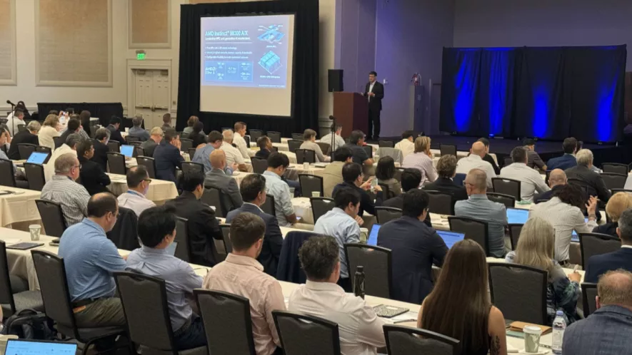
Semiconductor Industry Overview
Career Advice from an Industry Veteran
Ask Me Anything: Transition from Academia to the Semiconductor Job Market
Panel Discussion with Recent Graduates
Introduction to ChipPath
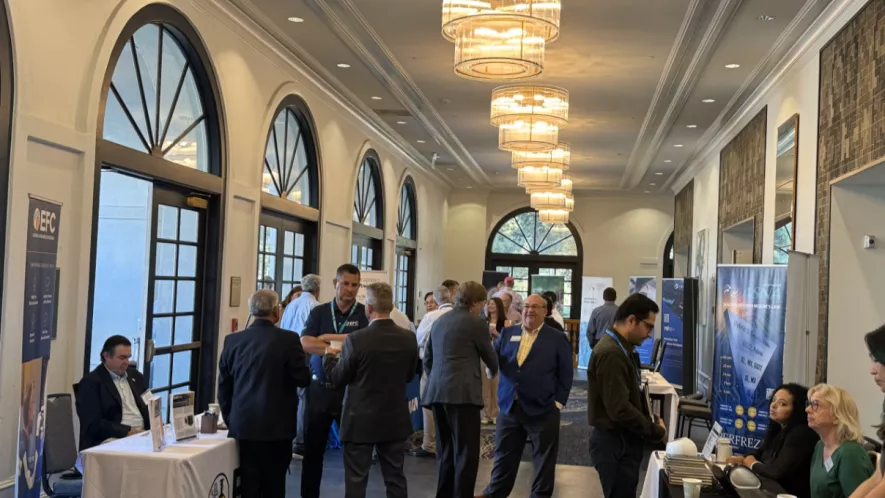
Sponsor Showcase
Facility Tour
Networking Lunch & Visiting Exhibitors
[PDS] Northeast Professional Development Seminar
—Organized by SEMI Northeast Chapter
—Hosted by NY Creates
Prepare for a Successful Career in the Semiconductor Industry
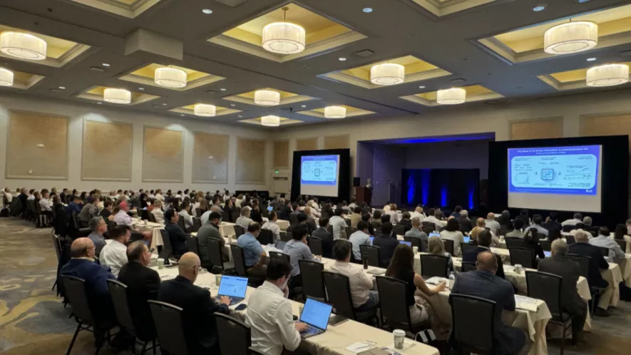
The Northeast Professional Development Seminar (PDS) is an in-person event designed to help students develop the skills, knowledge, and professional connections needed to thrive in today’s high-tech workforce. Through industry presentations, career-focused discussions, and networking opportunities, attendees will gain valuable insights into careers in the semiconductor industry and learn how to position themselves for success.