Registration
Attendance at this event is by invitation only.
Registration is complementary (free) with your invitation.
Travel
Venue
GES Taiwan 2026 will be held at the Junior Ballroom, 5F, Taipei Marriott Hotel, in conjunction with SEMICON Taiwan 2026.
Hotel
Taipei Marriott Hotel
SEMI has arranged a special group rate for GES attendees.
Introduction
Following the inaugural GES in Tokyo in 2025, the GES returns in 2026 as the Executive Summit on Energy and Sustainability to be held in Taipei, Taiwan, bringing together senior executives from across the semiconductor value chain to drive collective progress on the industry's most pressing energy and decarbonization challenges.
This is an invitation-only event.
Day at a Glance
Building on the foundational commitments established at GES 2025 in Tokyo, this year's summit is structured around two sessions. All times are Taiwan Standard Time.
Morning Session (8:00 AM - 12:20 PM) + Lunch
Sponsored by Google
Face-to-face GES Executive Council (GESEC) meeting to review progress and challenges on GES 2025 calls-to-action driven initiatives and to also lay out 2027 direction.
Afternoon Session (1:30 PM - 5:30 PM) + Happy Hour and Networking
To be Sponsored by leading Taiwan and Global companies (inclusion of names pending respective branding approvals)
This impactful session establishes the context for Taiwan's energy transition and semiconductor decarbonization. By pairing government keynotes and industry presentations with a public-private panel discussion, the session aims to surface key challenges and opportunities that can shape critical topics for inclusion in future GES Executive Council (GESEC), Semiconductor Climate Consortium (SCC) and/or Energy Collaborative (EC) initiatives.
Taipei Marriott Hotel,
Junior Ballroom, 5F (in conjunction with SEMICON Taiwan 2026)
Zhongshan District, Taipei City
Taiwan
Open to GESEC members, SCC and EC leaders, invited executives. By invitation. Not transferable.
Arrival and Registration


Opening Remarks
Keynote Speaker
Initiative-Level Reviews (break included)
Council Roundtable: 2027 Direction
Closing: Key Themes and Next Steps
Lunch
Open to GESEC members, SCC and EC leaders, and invited industry and government executives. By invitation.
Arrival and Registration
Welcome Attendees and Introduction to Agenda
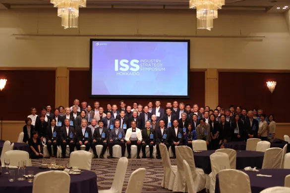
Welcome Dignitaries, Official Opening of the GES, and Group Photo
MOEA Keynote on Energy
GES: Addressing Emissions and Energy (SCC and EC)
Energy Strategy: Key Challenges and Opportunities in Taiwan
Break
Energy Strategy: Semiconductor Industry in Taiwan
Powering Sustainable Growth: Energy and Sustainability
Clean Electricity - Taiwan Call to Action
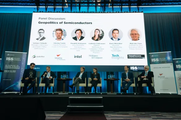
Panel Discussion: Opportunities for Public and Private Partnership (PPP) for Energy Transition in Taiwan
Moderator: Lora Ho, Consultant, Corporate Sustainability Office, TSMC
Panelists: Government, Industry, Developer, and Finance sector representatives
Closing Remarks
Happy Hour and Networking

Contact
For inquiries, please contact David Chiang at [email protected].