등록안내

※ 사전등록 마감일: 2026년 9월 2일(수) 오후 5시
[사전등록]
- SEMI회원사: 198,000
- 비회원사: 231,000
[현장등록]
- SEMI 회원사/비회원사: 253,000
※ 부가세 포함
OVERVIEW
- 교육명: SEMI 반도체테스트기술교육 2026
- 일정: 2026년 9월 9일(수) 오전 9시 – 오후 5시 10분
- 장소: 수원컨벤션센터 205, 206호
- 주최: SEMI Korea
NOTICE
- 참석확인증은 교육 종료 이후 SEMI Korea 통합등록사이트(semikrprogram.com)에서 사후설문조사를 완료하시면 발급됩니다.
- 등록비에는 교재비가 포함되어 있으며 교육 당일 교재를 현장에서 수령하실 수 있습니다.
- 점심식사 및 주차비는 제공되지 않습니다.
- 교육내용 및 순서는 강사 사정에 의하여 임의로 변경될 수 있습니다.
- 본 교육은 고용노동부 환급과정이 아닙니다.
CONTACT
- 문의: SEMI 프로그램팀 ([email protected])
TESTIMONIALS (2025)
- 업계 전반의 시장 동향과 기술 경향을 파악할 수 있었습니다.
- 기술적 내용을 쉽게 설명해 현업 테스트 과정 및 핵심 항목을 체계적으로 파악할 수 있었습니다.
- 업종 정보 및 실무 이해도 향상에 도움이 되었습니다.
대한민국
수원컨벤션센터
등록확인

Semiconductor Test and Market
• Semiconductor History and Market
• Integrated Circuit Design and TEST
• ATE Test System Architecture
• AI Semiconductor Trend and Challenges of Test
Break
Power & Analog Test Introduction
LED driver, PMIC, BMIC, IGBT, Silicon Carbide등 Mobile, Automotive향 Power application의 전반적인 구조 및 동작을 설명하고 test에 필요한 기본적인 요소를 이해하도록 한다. 또한 이를 측정하기 위한 ATE hardware및 device의 신뢰도를 최대화할 test 방법 및 환경에 대해 설명한다.
Break
Power & Analog Test Introduction
Lunch
Interface/ DIB/ Socket/ Prober
반도체 검사 공정의 핵심 설비중의 하나인 TESTER 성능을 손실 없이 사용하기 위해서는 Test Socket, DIB(Device Interface Board), Probe Card 등의 interface 제품의 올바른 선택과 사용은 대단히 중요하며 특히 underkill일 때의 품질 issue 또는 overkill일 때의 양품 손실 등 품질과 비용측면에서 매우 큰 영향을 끼치는 핵심 구성품이라 할 수 있다. 기초적인 기능과 동작을 이해하고 사용자 입장에서의 올바른 제품의 선택을 위해 고려해야 할 사항들과 개발자 입장에서 설계와 개발 시 우선하여 관심을 가져야 할 부분을 살펴본다.
Break
Interface/ DIB/ Socket/ Prober
Break
DRAM:Wafer & Package
- Test Introduction
- Wafer Test Process Overview
- Package Test Process Overview
- Memory Test Hardware System Introduction
break
DRAM:Wafer & Package
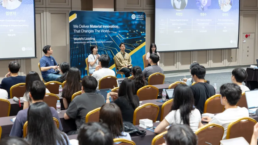
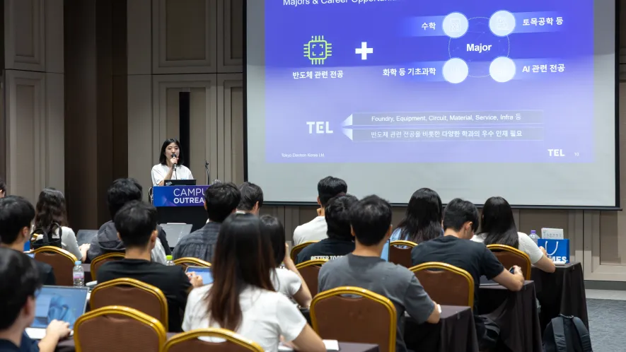
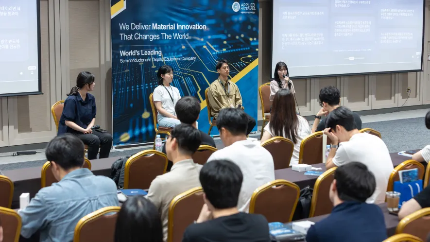
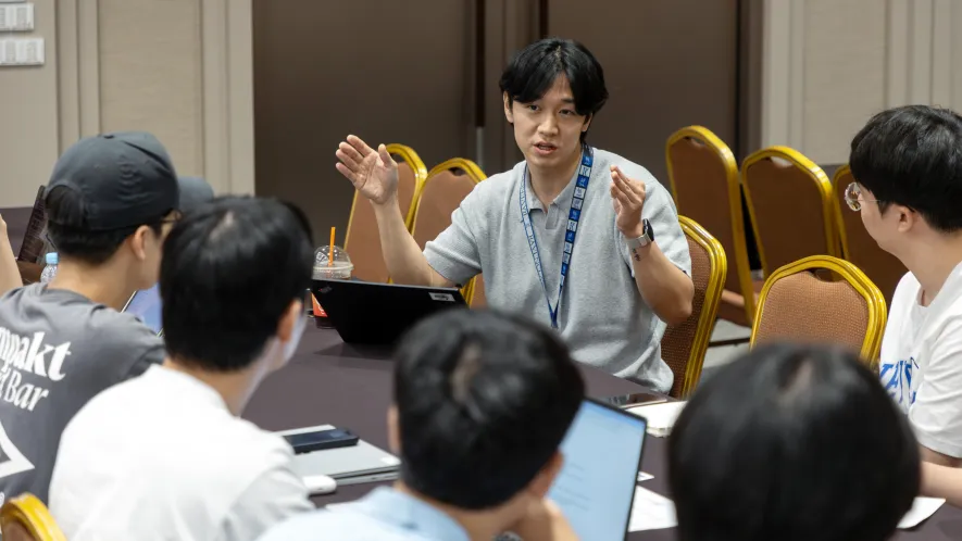
SEMI 반도체테스트기술교육은 AI 시대에 더욱 중요해지는 반도체 테스트 기술을 중심으로, 반도체 테스트 산업 및 시장 동향부터 ATE(Test System), Power & Analog Test, Interface(DIB·Socket·Probe Card), DRAM Wafer & Package Test까지 핵심 내용을 폭넓게 다루는 실무 중심 교육입니다. 최신 AI 반도체 테스트 트렌드와 메모리 테스트 기술을 비롯한 현업 적용 사례를 통해 실무 이해도를 높이고, 반도체 테스트 분야 엔지니어의 전문성 향상과 직무 역량 강화를 지원합니다.