downloadGroupGroupnoun_press release_995423_000000 copyGroupnoun_Feed_96767_000000Group 19noun_pictures_1817522_000000Member company iconResource item iconStore item iconGroup 19Group 19noun_Photo_2085192_000000 Copynoun_presentation_2096081_000000Group 19Group Copy 7noun_webinar_692730_000000Path
주요 콘텐츠로 건너뛰기
Default Banner Image

대한민국

Registration

Registration

※ 사전등록 마감일: 2026년 7월 8일 (수), 오후 5시 (한국 표준시 기준)

 Early BirdOn siteGroup
SEMI MemberKRW 308,000KRW 385,000KRW 275,000
Non MemberKRW 363,000KRW 330,000

※ 5인 이상 등록 시 단체등록비가 적용됩니다.
※ 단체등록은 SEMI Korea 프로그램팀([email protected])으로 문의 바랍니다.


Registration
대한민국 APS 2026 비즈니스 기술

OVERVIEW

  • 일시: 2026년 7월 15일(수) 8:30-17:00 
  • 장소: 수원컨벤션센터 3층 컨벤션홀 1
  • 언어: 한국어/영어 (동시통역 제공)  


SPONSORS


NOTICE

  • 아젠다는 연사 사정에 의하여 임의로 변경될 수 있습니다.
  • 발표자료는 연사의 배포 동의를 얻은 자료에 한하여 행사 종료 후 SEMI Korea 프로그램 등록사이트(https://semikrprogram.com)에 로그인하셔서 다운로드하실 수 있습니다.
  • 주차비는 제공되지 않습니다.  


CONTACT

대한민국
수원컨벤션센터 3층 컨벤션홀 1

8:30 am - 9:00 am

Welcome Reception

9:00 am - 9:30 am
Greg Roh
Greg Roh
Head of Research Center
Hyundai Motor Securities

2026 Outlook for the Advanced Packaging Industry
9:30 am - 10:00 am
Chee ping Lee
Chee ping Lee
Managing Director, Strategic & Technical Marketing, Advanced Packaging
Lam Research

Making 3DIC Manufacturable for AI: From Vertical Integration to Scalable Production

As AI systems push requirements for higher bandwidth, lower power, and increased integration density, 3D integrated circuits (3DIC) are moving rapidly from development to production. However, scaling 3DIC introduces complex application challenges across the manufacturing flow, where process interactions and control become critical.
This talk examines key 3DIC applications and process challenges, including high aspect ratio TSV etch, void free TSV fill, and dielectric deposition, required for reliable wafer and die level stacking. Emerging applications such as inter die gap fill for advanced chiplets integration and plasma dicing for improved yield, edge quality, and die strength further increase integration complexity and productivity demands.
The presentation highlights Lam Research innovations across etch, deposition and clean processes that enable tighter process windows, improved uniformity, and higher throughput. In addition, equipment intelligence and data driven control are increasingly essential to enhance yield learning and manufacturing productivity. Together, these advances are enabling scalable, high volume 3DIC manufacturing for next generation AI systems.

※ 연사정보

10:00 am - 10:30 am
Ingu Yin Chang
Yin Chang
ASE

Advanced Packaging: Enabling AI at Scale

The future of compute will not be defined by silicon alone. As AI reshapes industries and economies, advanced packaging has become the foundation of the next era of innovation, enabling unprecedented gains in performance, efficiency, and scale. During his keynote, Yin Chang will explore how breakthroughs in heterogeneous integration, chiplets, and advanced manufacturing are transforming bold AI ambitions into deployable systems, and why AI leadership will depend not only on compute power, but on the ability to integrate and manufacture at scale.
※ 연사정보

10:30 am - 11:00 am
Shinji Baba
Shinji Baba
Vice President / Head of ATJ R&D Center
Amkor Japan

Advanced Power Module Packaging Technologies

The rapid electrification of automotive and industrial systems is placing increasingly stringent demands on power semiconductor devices in terms of voltage capability, thermal performance, reliability, and system integration. This presentation reviews recent trends in power devices and power module packaging technologies aimed at improving performance while addressing cost and manufacturability constraints.
First, the fundamental differences between digital and power devices are outlined, followed by an overview of power device applications based on silicon (Si), silicon carbide (SiC), and gallium nitride (GaN) technologies, together with Amkor’s product portfolio.
Next, power module packaging technologies are discussed with a focus on key electrical and thermal challenges. Representative solutions, including advanced interconnects, cooling architectures, and embedded power modules, are introduced, along with a brief overview of Amkor’s technology roadmap.
Finally, the role of the Amkor Technology Japan R&D Center in supporting open innovation and global collaboration is briefly discussed.

※ 연사정보

11:00 am - 11:20 am

Networking Break

11:20 am - 12:30 pm

Panel Discussion

12:30 pm - 1:30 pm

Lunch

1:30 pm - 2:00 pm
minwoo rhee
Minwoo Rhee
Master
Samsung Electronics

Advanced Packaging Technology for AI/HPC

The presentation explores advanced packaging technologies designed to meet the escalating performance and power efficiency demands of AI and High-Performance Computing (HPC). To overcome the limitations of traditional semiconductor architectures, System Technology Co-Optimization (STCO) is introduced as a critical framework for managing thermal crosstalk and enhancing heterogeneous integration. The discussion highlights key innovations, including Customized HBM (cHBM) for optimized base-die performance and Samsung's 2.xD packaging portfolio, which encompasses Cube S, Cube E, and Cube R. Specifically, the 2.3D Cube E leverages panel level packaging to enable larger interposers and increased HBM integration, significantly improving productivity and reducing silicon fab burdens. The technical achievements in PLP—such as precise warpage control and the realization of fine RDL patterns (2/2μm)—are detailed to demonstrate their viability for large-scale AI chips. Furthermore, the roadmap extends toward 3D integration and Co-Packaged Optics (CPO) to maximize bandwidth and energy efficiency. Finally, the importance of an ecosystem-wide collaboration is emphasized as the driver for future innovation in "More than Moore" technology. These advancements collectively provide a scalable path toward the next generation of AI hardware acceleration.
※ Biography

2:00 pm - 2:30 pm
YASUSHI ARAKI
Yasushi Araki
Corporate Officer, GM(General Manager) of R&D Div.
SHINKO ELECTRIC INDUSTRIES

Latest Development Status of Glass Core Build-up Substrate

Glass core substrates exhibit low CTE and significantly higher rigidity than conventional organic substrates and are therefore regarded as promising core materials for next-generation build-up packages. However, a major challenge lies in the occurrence of SeWaRe defects (delamination in glass), which arise from thermal stresses induced by the mismatch in the coefficients of thermal expansion (CTE) between the glass material and the build-up resin.
To mitigate this issue, we proposed a structure in which the corner regions of each individual piece are formed from resin. However, considering the thermal history during chip mounting, it became evident that the suppression effect was insufficient. Therefore, an edge‑protection material was applied to relieve the stress concentrated at the edges of each individual piece. As a result, it was confirmed that SeWaRe defects could be effectively suppressed even under thermal loading.
Through these efforts, we successfully developed a glass core build-up package substrate incorporating 11 layers of single‑sided copper wiring (22 layers in total).

※ 연사정보

2:30 pm - 3:00 pm
Sandeep Sane
Sandeep Sane
Vice President
Lightmatter

Beyond Moore's Law: How Silicon Photonics and Advanced Packaging Are Redefining HPC

AI and data-intensive workloads are outpacing what conventional semiconductor technology can deliver. Two innovations are stepping in to close the gap: Silicon Photonics, which brings optical-speed, low-power data transmission into the data center, and Advanced Packaging, which uses chiplets and 2.5D/3D integration to maximize performance and efficiency at the chip level.
This talk examines how these complementary technologies are reshaping HPC architecture—covering their current state, how they work in tandem, and the key technical and commercial barriers to large-scale adoption.
※ 연사정보

3:00 pm - 3:30 pm
Amit Oren
Amit Oren
Director CPO Packaging
NVIDIA

CPO Packaging: Challenges and Opportunities

Co-packaged optics (CPO) is emerging as a key enabler for scaling bandwidth while containing power and cost in next-generation AI and cloud infrastructure. By moving optical engines closer to the switch ASIC and shortening high-speed electrical reaches, CPO can reduce SerDes power, ease signal-integrity constraints, and increase overall front-panel bandwidth density. However, delivering these benefits at volume requires new approaches across package architecture, manufacturing, and system integration.
This presentation reviews the main packaging challenges that must be solved to industrialize CPO, including thermal management and heat spreading near high-power silicon, fiber attach and optical alignment tolerances, photonics/laser integration choices, high-density optical and electrical I/O, substrate and interposer selection, and reliability risks such as warpage, CTE mismatch, and contamination control. Test and rework strategy, yield learning, and supply-chain readiness (materials, assembly, and metrology) are highlighted as practical barriers to adoption.
The talk also outlines opportunities created by CPO packaging innovations—such as modular optical tiles, standardized fiber interfaces, advanced lid/heat-sink concepts, and co-design of electrical, mechanical, and optical domains—to unlock higher radix switches and lower system power. Attendees will leave with a structured view of technology tradeoffs, a roadmap of near-term versus long-term packaging options, and actionable considerations for bringing CPO from prototypes to deployable products.

※ 연사정보

3:30 pm - 3:50 pm

Networking Break

3:50 pm - 5:00 pm

Panel Discussion

이번 Advanced Packaging Summit은 “Packaging the Future of AI – From Silicon to Photon”을 테마로, AI 시대 패키징 기술의 진화 방향과 산업적 의미를 심도 있게 조망합니다. 업계를 선도하는 전문가들의 발표를 통해 AI 반도체 수요 확대에 따른 시장 변화와 첨단 패키징 구현을 위한 핵심 기술들을 폭넓게 살펴보고, 실리콘 기반 집적 기술부터 광 기반 인터커넥트로 이어지는 혁신 흐름을 다룰 예정입니다. 또한, 각 세션별 패널 토의를 통해 실제 적용 사례와 기술적 과제, 산업 전반의 협력 가능성을 공유하며, AI 시대 패키징 기술이 창출할 새로운 비즈니스 기회와 전략적 인사이트를 함께 모색하고자 합니다.  

8:30 am - 5:00 pm Off Add to Calendar 2026-07-15 08:30:00 2026-07-15 17:00:00 ADVANCED PACKAGING SUMMIT 2026 이번 Advanced Packaging Summit은 “Packaging the Future of AI – From Silicon to Photon”을 테마로, AI 시대 패키징 기술의 진화 방향과 산업적 의미를 심도 있게 조망합니다. 업계를 선도하는 전문가들의 발표를 통해 AI 반도체 수요 확대에 따른 시장 변화와 첨단 패키징 구현을 위한 핵심 기술들을 폭넓게 살펴보고, 실리콘 기반 집적 기술부터 광 기반 인터커넥트로 이어지는 혁신 흐름을 다룰 예정입니다. 또한, 각 세션별 패널 토의를 통해 실제 적용 사례와 기술적 과제, 산업 전반의 협력 가능성을 공유하며, AI 시대 패키징 기술이 창출할 새로운 비즈니스 기회와 전략적 인사이트를 함께 모색하고자 합니다.   대한민국 수원컨벤션센터 3층 컨벤션홀 1 SEMI.org [email protected] Asia/Seoul public Asia/Seoul 등록 바로가기
Event format
Promote in calendar
Off

첨단 공정, 컴퓨팅 및 메모리 수요에 힘입어 웨이퍼 팹 및 패키징 재료 부문 모두 성장

​

​

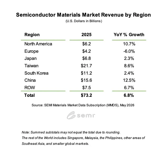
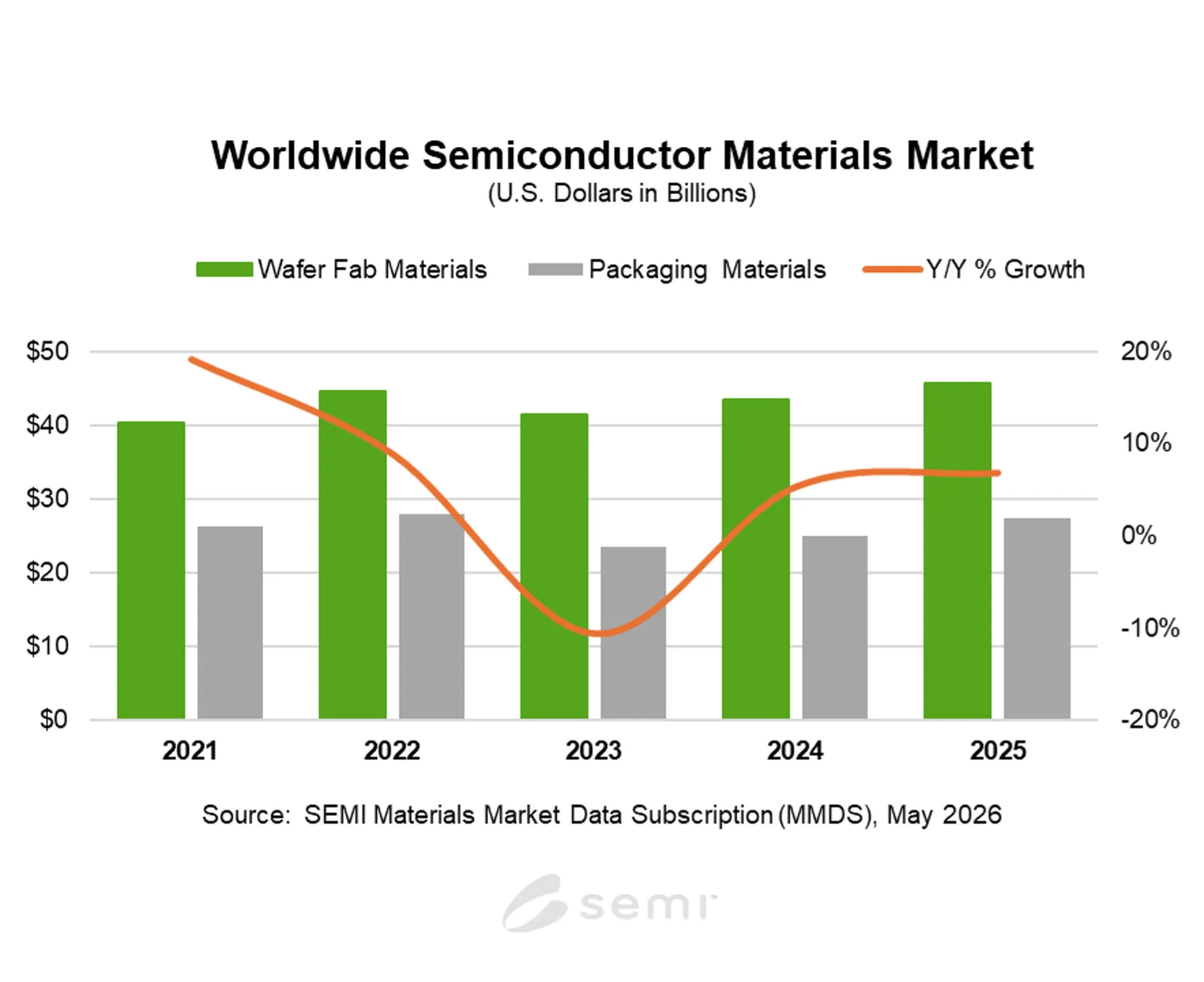
글로벌 전자 산업 공급망을 대표하는 산업 협회인 SEMI는 2025년 글로벌 반도체 재료 시장 매출은 전년 대비 6.8% 증가한 732억 달러를 기록했다고 발표했다. 이번 성장은 웨이퍼 팹 재료와 패키징 재료 부문 모두의 증가세에 힘입은 것으로, 공정 복잡도 상승, 첨단 노드 수요 확대, 고성능 컴퓨팅 및 고대역폭 메모리 제조에 대한 지속적인 투자가 주요 요인으로 작용했다.

웨이퍼 팹 재료 매출은 5.4% 증가한 458억 달러를 기록했다. 포토마스크, 포토레지스트 및 부속 재료를 포함한 리소그래피 관련 재료와 습식 화학물질은 공정 집약도 증가와 더욱 엄격해진 리소그래피 요구사항으로 인해 재료 소비가 확대되면서 두 자릿수의 높은 성장률을 보였다.

패키징 재료 매출은 2025년 9.3% 증가한 274억 달러를 기록했다. 기판과 본딩 와이어가 성장을 주도했으며, 본딩 와이어의 경우 금 가격 상승이, 기판의 경우 첨단 기판 수요 확대가 주요 성장 요인으로 작용했다.


대만은 2025년 217억 달러의 매출을 기록하며 16년 연속 세계 최대 반도체 재료 소비 지역의 지위를 유지했다. 중국은 두 자릿수 성장세에 힘입어156억 달러로 2위를 차지했으며, 한국은 112억 달러로 그 뒤를 이었다. 유럽을 제외한 모든 지역에서 전년 대비 증가세가 나타났으며, 주요 지역 중에서는 중국과 북미가 가장 높은 성장률을 기록했다.


​

​

이번 발표에 인용된 SEMI의 재료시장 데이터 구독 서비스(Materials Market Data Subscription, MMDS)는 연간 매출 자료와 함께 10년간의 과거 데이터 및 2년간의 전망을 제공한다. 연간 구독 서비스에는 재료 부문의 분기별 업데이트가 포함되며, 북미, 유럽, 일본, 대만, 한국, 중국, 기타 지역 등 7개 시장 지역별 매출 자료를 제공한다. 또한 실리콘 출하량과 포토레지스트, 포토레지스트 부속 재료, 공정 가스 및 리드프레임 매출에 대한 상세한 과거 데이터도 포함된다.

등록안내

Registration

등록이 모두 정원 마감되었습니다. (현장등록도 불가합니다.)


사전등록 마감일: 2026년 6월 12일(금) 오후 5시   

[사전등록]  

  • SEMI회원사: 165,000  
  • 비회원사: 198,000   

[현장등록]  

  • SEMI 회원사/비회원사: 220,000   

 ※ 부가세 포함

Registration
대한민국 PKG Tutorial 2026 기술 트레이닝

OVERVIEW 

  • 교육명: SEMI 반도체패키징기술교육 2026
  • 대상: 패키징 관련 경력 5년 이상 엔지니어
  • 일정: 2026년 6월 17일(수) 오전 9시 - 오후 5시
  • 장소: 수원컨벤션센터 305호
  • 주최: SEMI Korea  


NOTICE 

  • 참석확인증은 SEMI Korea 통합등록사이트(www.semikrprogram.com)에서 사후설문조사를 완료하시면 발급됩니다.
  • 등록비에는 교재비가 포함되어 있으며 당일 현장에서 수령하실 수 있습니다.
  • 점심식사 및 주차비는 제공되지 않습니다.
  • 교육내용 및 순서는 강사 사정에 의하여 임의로 변경될 수 있습니다.
  • 본 교육은 고용노동부 환급과정이 아닙니다.


CONTACT


TESTIMONIALS

  • HBM 및 WLP 공정별 상세 소개에서 전문성이 돋보였습니다.
  • HBM과 SiP에 대한 이해도 향상에 도움이 되었습니다.
  • 반도체 패키징에 대한 최신 트렌드와 기술 동향에 대한 정보 습득에 도움이 되었습니다. 


2025 Participating Companies—

  • 3M
  • Apple
  • ASM
  • ASML
  • ATI
  • Auros Technology
  • Bosch Rexroth
  • Corning
  • DuPont
  • Evatec
  • EVO
  • GigaVis
  • Hitachi High-Tech
  • Hysolem
  • INFICON
  • INNOX Advanced Materials
  • ITM Semiconductor
  • Justek
  • KCC Silicone
  • KLA
  • Koh Young Technology
  • Lam Research
  • LG Innotek
  • MEERE Company
  • Nextin
  • Park Systems
  • Pilz
  • Point Engineering
  • Samsung Electronics
  • Samsung SDI
  • SFA Semicon
  • TeraView
  • VERMES Microdispensing
  • WONIK IPS
  • Yamaha Robotics
  • Yield Engineering Systems


대한민국
수원컨벤션센터

9:00 am - 10:00 am
서민석.png
서민석
연구소장
Camtek

SiP with HBM | Process of WLP(HBM) ①

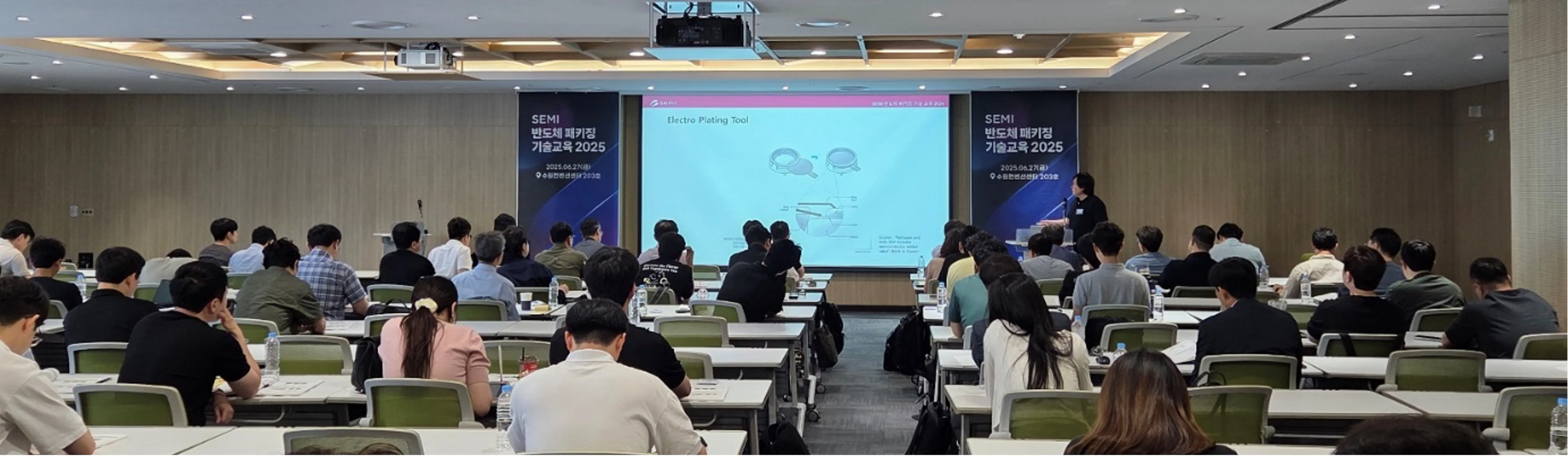
5G, 자율주행, 클라우드 컴퓨팅 등 때문에 반도체에 대해 고속, 고용량, 저전력 특성의 요구가 더욱 더 커지고 있다. 지금까지는 이러한 요구를 반도체 공정의 스케일 다운을 통해서 만족시킬 수 있었지만, 최근 Chat GPT 등 인공 지능의 활용이 늘어나면서 데이터의 사용량은 급증하게 됨에 따라 반도체의 스케일 다운만으로는 이러한 요구 사항을 만족시키기 어렵고, 적층, 이종 접합 등의 첨단 반도체 패키지 기술이 필요하게 되었다. 본 과정에서는 웨이퍼 레벨 패키지(WLP, wafer level package), 적층(stack) 패키지, 시스템 인 패키지(SiP, System in Package) 등의 첨단 패키지 기술 트렌드에 대해서 심도 있게 고찰하려 한다. 특히 TSV 적층 기술과 웨이퍼 레벨 패키지 기술을 이용한 HBM(High Bandwidth Memory)의 의미와 공정을 이야기하고, HBM을 이용한 시스템 인 패키지기술을 설명하려 한다. 그리고, 칩릿(Chiplet)을 이용한 시스템 인 패키지 기술의 필요성과 이를 위한 핵심 기술에 대해서도 정리하려 한다.

※ 연사정보

10:00 am - 10:10 am

Break

10:10 am - 11:10 am
서민석.png
서민석
연구소장
Camtek

SiP with HBM | Process of WLP(HBM) ②

11:10 am - 11:20 am

Break

11:20 am - 12:20 pm
서민석.png
서민석
연구소장
Camtek

SiP with HBM | Process of WLP(HBM) ③

12:20 pm - 1:40 pm

Lunch

1:40 pm - 2:40 pm
김종훈 TL
김종훈
TL
SK hynix

Advanced Packaging for High Performance Computing System ①

AI 시대의 도래와 함께 LLM과 같은 초거대 AI 모델의 학습 및 추론을 위한 High Performance Computing(HPC)의 중요성이 빠르게 증가하고 있다. 그러나 기존의 미세공정 scaling만으로는 연산 성능 향상에 한계가 발생하고 있으며, 메모리 대역폭, 전력 효율, 칩 간 데이터 전송과 같은 문제가 핵심 과제로 부상하고 있다. 이러한 한계를 극복하기 위한 핵심 기술 중 하나가 바로 Advanced Packaging 기술이다. 본 강의에서는 AI 시대 HPC 시스템이 요구하는 성능 특성과 시스템 구조를 먼저 이해하고, 이를 가능하게 하는 다양한 Advanced Packaging 기술들을 체계적으로 설명하고자 한다. 먼저 2.5D/3D 패키징 기술과 TSV, silicon interposer, hybrid bonding과 같은 핵심 요소 기술을 살펴보고, GPU와 HBM을 초고속으로 연결하기 위한 최신 패키지 구조를 분석한다. 이어서 Chiplet architecture, CoWoS, Foveros, SoIC, Fan-Out Packaging(FOPLP/FOWLP)과 같은 산업 적용 사례를 소개하며, 고대역폭·저전력 구현을 위한 패키지 기술 방향을 설명하고자 한다.

※ 연사정보

2:40 pm - 2:50 pm

Break

2:50 pm - 3:50 pm
김종훈 TL
김종훈
TL
SK hynix

Advanced Packaging for High Performance Computing System ②

3:50 pm - 4:00 pm

Break

4:00 pm - 5:00 pm
김종훈 TL
김종훈
TL
SK hynix

Advanced Packaging for High Performance Computing System ③

SEMI 반도체 패키징 기술 교육은 패키징 분야 경력 엔지니어를 위한 심화 교육 프로그램입니다. 본 교육은 패키징 기술에 대한 기본 이해를 갖춘 장비사, 소재사 및 연구기관의 경력 엔지니어를 대상으로, HBM을 포함한 첨단 패키징 기술과 주요 응용 사례를 폭넓게 소개함으로써 산업 종사자들의 실질적인 실무 역량 강화를 목표로 기획되었습니다.

9:00 am - 5:00 pm Off Add to Calendar 2026-06-17 09:00:00 2026-06-17 17:00:00 SEMI 반도체패키징기술교육 2026 SEMI 반도체 패키징 기술 교육은 패키징 분야 경력 엔지니어를 위한 심화 교육 프로그램입니다. 본 교육은 패키징 기술에 대한 기본 이해를 갖춘 장비사, 소재사 및 연구기관의 경력 엔지니어를 대상으로, HBM을 포함한 첨단 패키징 기술과 주요 응용 사례를 폭넓게 소개함으로써 산업 종사자들의 실질적인 실무 역량 강화를 목표로 기획되었습니다. 대한민국 수원컨벤션센터 SEMI.org [email protected] Asia/Seoul public Asia/Seoul 등록 바로가기
Event format
Promote in calendar
Off

AI 기반 수요와 광범위한 회복 조짐이 혼조세 속에서도 글로벌 실리콘 웨이퍼 출하량 견인   

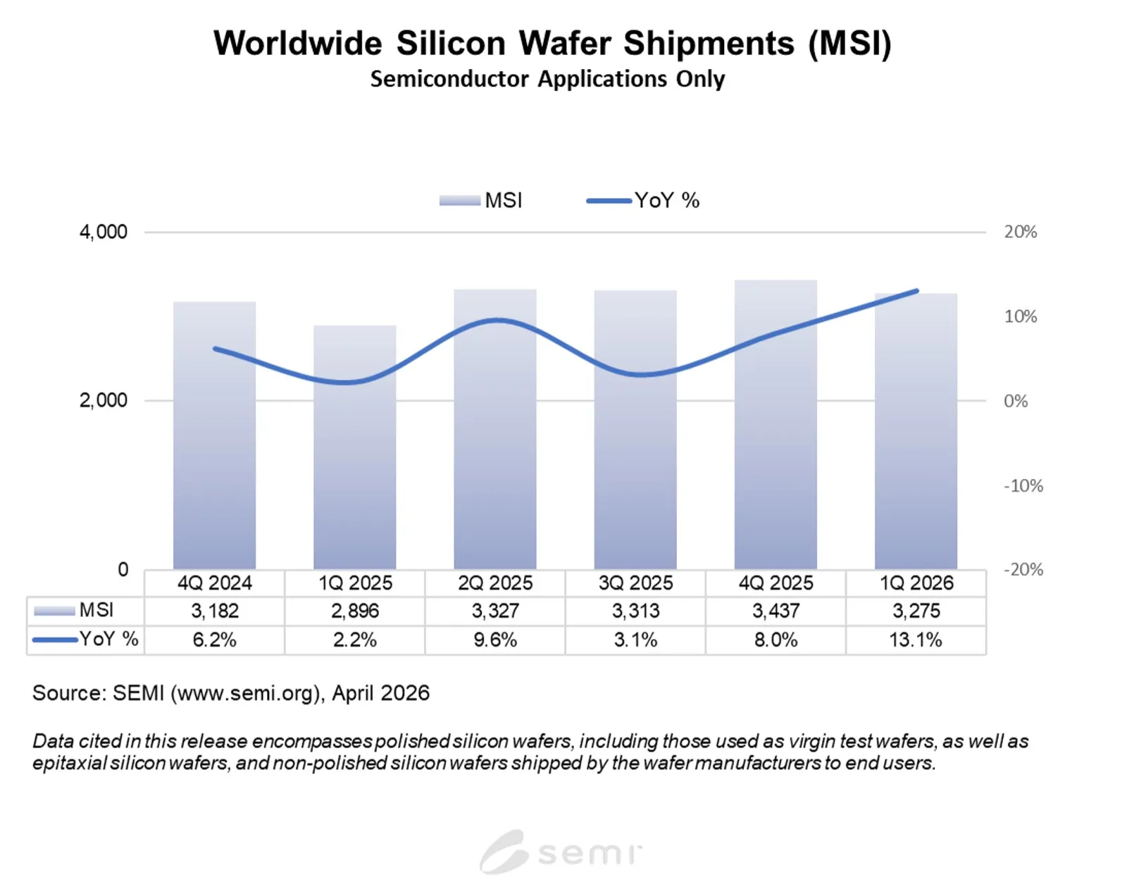
글로벌 전자 산업 공급망을 대표하는 산업 협회인 SEMI는 2026년 1분기 전 세계 실리콘 웨이퍼 출하량이 32억 7,500만 제곱인치를 기록했다고 발표했다. 이는 2025년 같은 분기의 28억 9,600만 제곱인치 대비 13.1% 증가한 수치다. 전 분기와 비교하면 2025년 4분기 34억 3,700만 제곱인치 대비 4.7% 감소했으며, 이는 일반적인 시즌적 요인에 따른 흐름으로 분석된다.   

SEMI SMG(Silicon Manufacturers Group) 회장이자 섬코(SUMCO) 영업·마케팅 부문 부총괄인 긴지 야다(Ginji Yada)는 “첨단 로직과 메모리를 포함하여 AI 데이터센터와 관련된 실리콘 웨이퍼 수요는 계속해서 강세를 보이고 있으며, 이제 전력 관리 반도체 분야로도 확대되고 있다”고 말했다. 그는 이어 “전반적인 실리콘 웨이퍼 수요는 개선됐지만, 회복세가 모든 분야에서 균일하게 나타나고 있는 것은 아니다. 특히 산업용 반도체 부문의 수요 회복세가 빠르다.”고 말하였다. 

실리콘 웨이퍼는 대부분의 반도체를 제조하는 데 사용되는 핵심 기초 소재로, 반도체는 모든 전자기기의 필수 부품이다. 고도로 정밀하게 가공된 얇은 원판 형태의 실리콘 웨이퍼는 최대 300mm 직경으로 생산되며, 대부분의 반도체가 제조되는 기판 소재로 활용된다.

SMG는 SEMI 전자재료 그룹(Electronic Materials Group, EMG) 산하의 소위원회로, 다결정 실리콘, 단결정 실리콘 또는 실리콘 웨이퍼 제조에 참여하는 SEMI 회원사에게 개방되어 있다. 여기에는 절단 웨이퍼, 연마 웨이퍼, 에피택셜 웨이퍼 등이 포함된다. SMG는 실리콘 산업과 관련된 주요 이슈에 대한 공동 대응을 촉진하고, 실리콘 산업 통계 개발을 포함한 다양한 활동을 지원한다.

Registration

Registration

※ 사전등록 일정: 2026년 5월 14일(목) ~ 6월 17일(수) 오후 5시


Registration Fee  

  • Early Bird
    • SEMI 회원사: KRW 180,000
    • 비회원사: KRW 240,000
  • On site
    • SEMI 회원사: KRW 300,000
    • 비회원사: KRW 300,000

※ 상기 등록비는 부가세가 포함된 가격입니다.

Registration
대한민국 GMIF 2026 비즈니스 경영진

OVERVIEW

  • 일시: 2026년 6월 23일(화) 12:30-17:00
  • 장소: 수원컨벤션센터 2층 202호  
  • 언어: 한국어/영어 (동시통역 제공)  


NOTICE

  • 아젠다는 연사 사정에 의하여 임의로 변경될 수 있습니다.
  • 발표자료는 연사의 배포 동의를 얻은 자료에 한하여 행사 종료 후 SEMI Korea 프로그램 등록사이트(https://semikrprogram.com)에 로그인하셔서 다운로드하실 수 있습니다.
  • 주차비는 제공되지 않습니다.  


CONTACT

대한민국
수원컨벤션센터

12:30 pm - 1:00 pm

Networking Reception

1:00 pm - 1:10 pm
Hyun Cha
차지현
대표
SEMI Korea

Opening

1:10 pm - 1:40 pm
Changwook-Kim
김창욱
파트너
Boston Consulting Group

Restructuring of the Semiconductor Industry Driven by AI and the Opportunities It Creates

The rapid expansion of AI is fundamentally reshaping the semiconductor industry, driving unprecedented investment in AI data centers, accelerating technological transitions, and redefining competitive dynamics across the ecosystem. At the same time, growing debates around the sustainability of AI-related investments and the potential risks of an AI bubble are creating new uncertainties for industry players.

Changwook Kim, Managing Director and Partner at BCG and leader of the semiconductor practice in Korea, will present on the “AI-Driven Restructuring of the Semiconductor Industry and the Opportunities it creates.” The session will cover AI data center investment trends and outlook, the impact of AI on the memory semiconductor market, recent changes across the semiconductor ecosystem including fabless, foundry, packaging, and memory technologies, and the strategic implications and opportunities for semiconductor companies.

※ 연사정보

1:40 pm - 2:10 pm
JY Kim
김지영
교수
서울대학교

Beyond Scaling: Building the Next-Generation AI Semiconductor Framework

AI is moving from large-scale model training toward inference and agent-based services. GPUs, HBM, and 2.5D interconnects have powered the first wave of AI acceleration, but the future is diversifying—bringing AI accelerators, CPUs, general-purpose memory, and on-die AI semiconductors into play. From a memory-centric view, the demand for massive capacity, ultra-fast speed, and wide I/O bandwidth is clear. Yet the most urgent challenge is low power. This talk will explore the current limits of DRAM core die technology in HBM and highlight new device structures designed to break through these bottlenecks. We will look at the shift beyond the traditional 1T1C DRAM cell toward oxide-semiconductor-based 2T0C architectures, advances in bonding methods, and the potential of glass substrates. We will also examine strategies for achieving low-power operation—from smarter architectures to heterogeneous integration of processors and memory—and discuss how these innovations open opportunities across devices, materials, equipment, and packaging. By framing these breakthroughs within a broader AI semiconductor technology framework, the session will provide a clear view of both the technical challenges and the strategic directions shaping the next era of global semiconductor innovation.

※ 연사정보

2:10 pm - 2:40 pm
Clark-Tseng
Clark Tseng
Sr. Director
SEMI

AI Demand Meets Capacity Reality: Semiconductor Infrastructure and Korea’s Role in the Next Investment Cycle

AI is reshaping the semiconductor industry from both the demand side and the infrastructure side. While AI accelerators, HBM, advanced logic, and data-center infrastructure continue to drive strong growth, the broader market remains uneven, with consumer-driven segments recovering more gradually and macro uncertainty still shaping investment decisions. This presentation will review the key market forces behind the current semiconductor cycle and examine how AI demand is translating into fab investment, capacity expansion, and equipment spending.
The discussion will highlight SEMI’s latest view of global fab investment, capacity growth, and regional expansion. It will also address why the next phase of growth depends not only on headline demand, but also on qualified capacity, technology migration, packaging and test readiness. With Korea’s leadership in memory and manufacturing execution, the presentation will place Korea’s role within the broader global infrastructure buildout supporting the AI era.

※ 연사정보

2:40 pm - 3:00 pm

Break

3:00 pm - 3:30 pm
Calvin Yong
Calvin Yong
Director
Yole Group

Packaging as the New Strategic Layer

As monolithic scaling approaches the physical and economic limits of Moore’s Law, Advanced Semiconductor Packaging (ASP) has transitioned from a routine backend process to the primary driver of microelectronic innovation. Driven by an unprecedented surge in demand for Artificial Intelligence (AI), high-performance computing (HPC), and 5G infrastructure, ASP has emerged as the new strategic layer in the global technology ecosystem, reshaping hardware architecture and market competition.
Through heterogeneous integration, advanced packaging techniques—such as 2.5D/3D stacking and fan-out wafer-level packaging—bypass single-die fabrication constraints. By combining disparate, optimized chiplets into a unified system, ASP fulfills the skyrocketing commercial need for massive interconnect densities, ultra-low latencies, and extreme thermal efficiencies.
Ultimately, semiconductor leadership is no longer defined solely by front-end lithography nodes, but by the ability to architect complex, multi-die systems. Packaging has effectively become the critical differentiator, supply chain constraint, and the ultimate bottleneck for future technological supremacy.

※ 연사정보

3:30 pm - 4:00 pm
사진_김병연
김병연
이사
NH투자증권

시차의 경제학-반도체 구조적 성장 속 글로벌 하반기 금융시장

4:00 pm - 4:45 pm

Panel Discussion

5:00 pm

Closing

반도체 산업은 이제 기술적 진보를 넘어, 글로벌 정치와 AI가 주도하는 복잡한 거시적 변화에 직면해 있습니다. Global Semiconductor Market Insight Forum은 이러한 환경 변화 속에서 반도체 생태계를 이끄는 주요 리더들이 모여, 산업을 견인하는 기술과 시장의 동인을 살펴보고 산업 투자 흐름에 대한 이해를 높일 수 있도록 마련한 포럼입니다.

특히 패널 디스커션을 통해 각기 다른 기술·시장·투자 관점에서 바라본 반도체 산업에 대한 인사이트를 공유함으로써, 단일 시각을 넘어 보다 입체적인 전략적 통찰을 제공할 예정입니다. 이를 통해 산업의 미래를 고민하는 C‑레벨 리더들이 한자리에 모여, 반도체 산업의 중장기 방향성과 비전에 대한 공감대를 형성할 수 있기를 기대합니다.

12:30 pm - 5:00 pm Off Add to Calendar 2026-06-23 12:30:00 2026-06-23 17:00:00 2026 Global Semiconductor Market Insight Forum 반도체 산업은 이제 기술적 진보를 넘어, 글로벌 정치와 AI가 주도하는 복잡한 거시적 변화에 직면해 있습니다. Global Semiconductor Market Insight Forum은 이러한 환경 변화 속에서 반도체 생태계를 이끄는 주요 리더들이 모여, 산업을 견인하는 기술과 시장의 동인을 살펴보고 산업 투자 흐름에 대한 이해를 높일 수 있도록 마련한 포럼입니다.특히 패널 디스커션을 통해 각기 다른 기술·시장·투자 관점에서 바라본 반도체 산업에 대한 인사이트를 공유함으로써, 단일 시각을 넘어 보다 입체적인 전략적 통찰을 제공할 예정입니다. 이를 통해 산업의 미래를 고민하는 C‑레벨 리더들이 한자리에 모여, 반도체 산업의 중장기 방향성과 비전에 대한 공감대를 형성할 수 있기를 기대합니다. 대한민국 수원컨벤션센터 SEMI.org [email protected] Asia/Seoul public Asia/Seoul
Event format
Promote in calendar
Off

Registration

Registration
과정일정교육비
회원사비회원사현장등록
기초과정6/10 (수)165,000원198,000원220,000원
심화과정  6/11(목) – 6/12(금)286,000원345,000원385,000원

※  부가세 포함 가격입니다.

  • 등록 및 결제 마감일: 2026년 5월 29일(금) 오후 5시
  • 등록 절차: 통합등록사이트(www.semikrprogram.com)) 접속 > 로그인 후 해당 프로그램 등록 신청 > 결제 > 등록완료
  • SEMI 회원사 확인 (바로가기)  
Registration
대한민국 SGT 2026 비즈니스 트레이닝

[OVERVIEW]

  • 교육명: SEMI 안전표준교육 2026 (상반기)
  • 일정: 2026년 6월 10일(수) – 12일(금)
  • 장소: 수원 컨벤션센터 202호
  • 주최: SEMI Korea
  • 문의: SEMI Korea 표준팀 (02-531-7899 / [email protected])  


[COURSE DETAILS]

  • 기초과정: SEMI S2 표준 내용 소개
    • 일정: 2026년 6월 10일(수)
    • 대상: 반도체 장비 개발/설계 엔지니어, 품질/규제 관련 실무자, 안전/환경(EHS) 관련 실무자
  • 심화과정: 비상정지 장치/안전 장치 설치 가이드라인, 화학물질/기계/방사/전기 설계 안전 가이드라인, 인체공학 설계 가이드라인, 위험성 평가 기법, 안전 인터록 회로 구성 등 안전표준 심화해설 (SEMI S2, S6, S8, S10, S14, S17, S22, S28)
    • 일정: 2026년 6월 11일(목) – 12일(금)
    • 대상: 경력 5년 내외 장비 개발/설계 엔지니어, 품질/규제 관련 실무자, 안전/환경(EHS) 관련 실무자


[NOTICE]

  • 교육내용 및 순서는 강사 사정에 의해 임의로 변경될 수 있습니다.
  • 본 교육은 반도체 제조사 및 장비사를 대상으로 운영되며, 3자 인증기관의 수강신청은 제한됩니다.
  • 본 교육은 2가지 과정(기초, 심화) 중 희망하시는 과정을 신청하여 수강하시는 과정입니다.
  • 본 교육은 고용노동부 환급과정이 아닙니다.
  • 등록비에는 중식과 교재비가 포함되어 있으며, 교재는 교육 당일 현장에서 수령하실 수 있습니다.
  • 주차비는 지원하지 않습니다.
  • 참석확인증은 교육 종료 후, 통합등록사이트(www.semikrprogram.com)에서 사후 설문조사를 완료하시면 발급됩니다.

대한민국
수원컨벤션센터

9:00 am - 9:40 am
전대영
전대영
부장
SGS Korea

SEMI S2 반도체 제조장비에 대한 환경, 보건, 안전 가이드라인 (개요)

9:40 am - 9:50 am

휴식

9:50 am - 10:40 am

SEMI S2 반도체 제조장비에 대한 환경, 보건, 안전 가이드라인 (Safety interlock, Emergency shutdown Ⅰ)

10:40 am - 10:50 am

휴식

10:50 am - 11:30 am

SEMI S2 반도체 제조장비에 대한 환경, 보건, 안전 가이드라인 (Safety interlock, Emergency shutdown Ⅱ)

11:30 am - 11:40 am

휴식

11:40 am - 12:30 pm

SEMI S2 반도체 제조장비에 대한 환경, 보건, 안전 가이드라인 (Electrical design, Fire protection)

12:30 pm - 1:30 pm

점심식사

1:30 pm - 2:10 pm

SEMI S2 반도체 제조장비에 대한 환경, 보건, 안전 가이드라인 (Ergonomic, Mechanical design, Ventilation Ⅰ)

2:10 pm - 2:20 pm

휴식

2:20 pm - 3:10 pm

SEMI S2 반도체 제조장비에 대한 환경, 보건, 안전 가이드라인 (Ergonomic, Mechanical design, Ventilation Ⅱ)

3:10 pm - 3:20 pm

휴식

3:20 pm - 4:00 pm

SEMI S2 반도체 제조장비에 대한 환경, 보건, 안전 가이드라인 (Environmental, Chemical, Radiation, Sound pressure level Ⅰ)

4:00 pm - 4:10 pm

휴식

4:10 pm - 4:50 pm

SEMI S2 반도체 제조장비에 대한 환경, 보건, 안전 가이드라인 (Environmental, Chemical, Radiation, Sound pressure level Ⅱ)

4:50 pm - 5:00 pm

Q&A

9:00 am - 9:40 am
임근영
임근영
부장
SAFE WORLD Engineering

SEMI S2 비상정지 장치 및 안전 장치 설치 가이드라인 해설 심화 (SEMI S2 Section 11,12)

9:40 am - 9:50 am

휴식

9:50 am - 10:40 am

SEMI S2 비상정지 장치 및 안전 장치 설치 가이드라인 해설 심화 (SEMI S2 Section 11,12)

10:40 am - 10:50 am

휴식

10:50 am - 11:30 am

SEMI S2 화학물질 안전 가이드라인 해설 심화 (SEMI S2 Section 14, 17, 21, 22, 23 and SEMI S6, S14)

11:30 am - 11:40 am

휴식

11:40 am - 12:30 pm

SEMI S2 화학물질 안전 가이드라인 해설 심화 (SEMI S2 Section 14, 17, 21, 22, 23 and SEMI S6, S14)

12:30 pm - 1:30 pm

점심식사

1:30 pm - 2:10 pm

SEMI S2 기계 안전 가이드라인 해설 심화 (SEMI S2 Section 11, 18, 19, 20 and SEMI S17, S28)

2:10 pm - 2:20 pm

휴식

2:20 pm - 3:10 pm

SEMI S2 기계 안전 가이드라인 해설 심화 (SEMI S2 Section 11, 18, 19, 20 and SEMI S17, S28)

3:10 pm - 3:20 pm

휴식

3:20 pm - 4:00 pm

SEMI S2 방사 관련 안전 가이드라인 해설 심화 (SEMI S2 Section 24, 25, 26)

4:00 pm - 4:10 pm

휴식

4:10 pm - 4:50 pm

SEMI S8 SESC 인체공학 설계 가이드라인 해설 및 예제

4:50 pm - 5:00 pm

Q&A

9:00 am - 9:40 am
박현준
박현준
차장
PCA

SEMI S22 반도체 제조장비의 전기 설계 안전 가이드라인 (Section 8 - 11)

9:40 am - 9:50 am

휴식

9:50 am - 10:40 am

SEMI S22 반도체 제조장비의 전기 설계 안전 가이드라인 (Section 12 - 15)

10:40 am - 10:50 am

휴식

10:50 am - 11:30 am

SEMI S22 반도체 제조장비의 전기 설계 안전 가이드라인 (Section 16 - 19)

11:30 am - 11:40 am

휴식

11:40 am - 12:30 pm

SEMI S22 반도체 제조장비의 전기 설계 안전 가이드라인(Section 20 - 22)

12:30 pm - 1:30 pm

점심식사

1:30 pm - 2:30 pm
박근용
박근용
이사
SZU Korea

SEMI S10에 기반한 위험성 평가 기법

2:30 pm - 2:40 pm

휴식

2:40 pm - 3:40 pm

SEMI S2 11장 안전 인터록 회로 구성에 대한 심화 학습

3:40 pm - 3:50 pm

휴식

3:50 pm - 4:40 pm

SEMI S2 RI 16 및 SEMI S2 11장에 의한 안전 인터록 회로 구성에 대한 심화 학습

4:40 pm - 5:00 pm

Q&A

- Standards

2026년 4월 13일(월) 오전 10시 등록 오픈! 

SEMI 안전표준은 반도체 제조장비의 안전한 설계 및 평가의 지침이 되는 핵심 산업표준으로, 전 세계 주요 반도체 제조사들에게 널리 사용되고 있습니다.  

오는 6월, SEMI 안전표준교육이 기초과정과 심화과정으로 나누어 개최됩니다. 표준의 기본적인 내용부터 올해 새롭게 마련된 SEMI S2 심화해설, 그리고 실무 지식까지 본 교육과 함께 SEMI 안전표준을 체계적으로 이해해 보세요.  

Off Add to Calendar 2026-06-10 00:00:00 2026-06-12 00:00:00 SEMI 안전표준교육 2026 (상반기) 2026년 4월 13일(월) 오전 10시 등록 오픈! SEMI 안전표준은 반도체 제조장비의 안전한 설계 및 평가의 지침이 되는 핵심 산업표준으로, 전 세계 주요 반도체 제조사들에게 널리 사용되고 있습니다.  오는 6월, SEMI 안전표준교육이 기초과정과 심화과정으로 나누어 개최됩니다. 표준의 기본적인 내용부터 올해 새롭게 마련된 SEMI S2 심화해설, 그리고 실무 지식까지 본 교육과 함께 SEMI 안전표준을 체계적으로 이해해 보세요.   대한민국 수원컨벤션센터 SEMI.org [email protected] Asia/Seoul public Asia/Seoul
Event format
Promote in calendar
Off

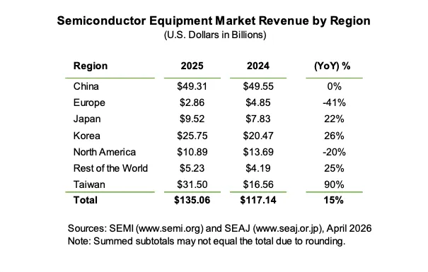
글로벌 전자 산업 공급망을 대표하는 산업 협회인 SEMI는 2025년 전 세계 반도체 장비 매출이 2024년 1,171억 달러에서 15% 증가한 1,351억 달러를 기록했다고 발표했다. 이번 성장은 첨단 로직과 메모리, AI 관련 생산능력 확대를 위한 지속적인 투자에 힘입은 것이다.

​

2025년 글로벌 전공정 반도체 장비 시장은 견조한 성장세를 보였다. 웨이퍼 가공 장비 매출은 12% 증가했으며, 기타 전공정 부문도 13% 성장했다. AI 관련 수요와 지속적인 노드 및 기술 전환에 힘입어 첨단 로직 및 메모리 생산능력에 대한 투자가 이러한 성장세를 견인하였다.

​

후공정 장비 부문 역시 2025년에 강한 성장세를 기록했다. AI 디바이스와 고대역폭메모리(HBM) 확대로 성능 요구와 테스트 강도가 높아지면서 테스트 장비 매출은 전년 대비 55% 급증했다. 또한 첨단 패키징 기술 도입이 계속 확대되면서 조립 및 패키징 장비 매출도 21% 증가했다.

​

SEMI의 CEO인 아짓 마노차는 “이러한 성장세는 AI가 첨단 반도체에 대한 수요를 가속화하면서, 업계의 생산능력 확장이 얼마나 빠르고 대규모로 진행되고 있는지를 보여준다”라고 말하며“웨이퍼 팹 투자부터 첨단 패키징과 테스트의 급부상에 이르기까지, 글로벌 생태계는 차세대 혁신을 뒷받침하기 위해 생산능력과 역량을 동시에 확대하고 있다”라고 덧붙였다.

​


지역별로는 2025년 반도체 장비 투자가 여전히 아시아에 집중됐으며, 중국·대만·한국이 합산 기준으로 글로벌 시장의 79%를 차지했다. 이는 2024년의 74%보다 높아진 수치다.

​

2025년 중국의 장비 투자는 493억 달러로 전년 대비 0.5% 감소하는 데 그쳤지만, 여전히 자국 반도체 기업들의 머츄어 공정 및 첨단 생산능력 투자를 지속하여 여전히 기록적인 수준에 근접했다. 대만의 장비 투자는 AI 및 HPC(고성능 컴퓨팅) 수요 기반의 생산능력 확대에 따라 전년 대비 90% 증가한 315억 달러로 사상 최고치를 기록했다. 한국은 HBM과 DRAM 투자 강세에 힘입어 26% 증가한 258억 달러를 기록했다.

​

일본은 자국 내 첨단 공정 제조 투자 지속에 힘입어 22% 증가한 95억 달러를 기록했다. 유럽은 자동차 및 산업 수요 부진이 이어지면서 41% 감소한 29억 달러로 2년 연속 역성장을 나타냈다. 북미는 앞선 생산능력 확대 이후 투자 속도가 조정되며 20% 감소한 109억 달러를 기록했다. 기타 지역은 신흥 반도체 생산 시장의 활동 확대에 힘입어 25% 증가한 52억 달러를 나타냈다.

​

이번 발표에 인용된 '글로벌 반도체 장비 시장 통계 보고서(Worldwide Semiconductor Equipment Market Statistics)'는 SEMI와 일본반도체장비협회 회원사들이 제출한 데이터를 기반으로 작성되며, 글로벌 반도체 장비 산업의 월별 매출 실적을 요약한 자료다.

Registration

Registration

※ 사전등록 마감일: 2026년 5월 7일(목) 오전 10시 


Registration Fee  

  • Early Bird
    • SEMI Member: KRW 308,000
    • Non-Member: KRW 363,000
  • On site
    • SEMI Member : KRW 385,000
    • Non-Member: KRW 385,000
  • Group
    • SEMI Member : KRW 275,000
    • Non-Member: KRW 330,000
      ※ 5인 이상 등록 시 단체등록비가 적용됩니다.

※ 단체등록은 SEMI Korea 프로그램팀([email protected])으로 문의 바랍니다.

Registration
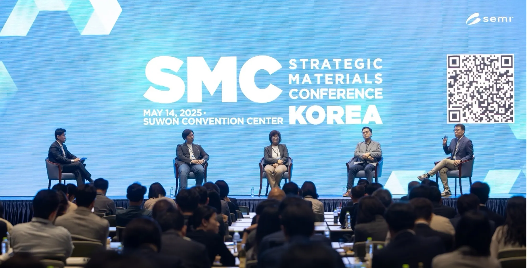
대한민국 SMC Korea 2026 비즈니스 기술

OVERVIEW

  • 일시: 2026년 5월 12일(화) 8:30-16:30  
  • 장소: 수원컨벤션센터 3층 컨벤션홀 2  
  • 언어: 한국어/영어 (동시통역 제공)  


NOTICE

  • 아젠다는 연사 사정에 의하여 임의로 변경될 수 있습니다.
  • 발표자료는 연사의 배포 동의를 얻은 자료에 한하여 행사 종료 후 SEMI Korea 프로그램 등록사이트(https://semikrprogram.com)에 로그인하셔서 다운로드하실 수 있습니다.
  • 주차비는 제공되지 않습니다.  


SPONSORS

SMC-Korea-2023-Sponsor_DW.jpg
SMC-Korea-2023-Sponsor_DS_0.jpg SMC-Korea-2023-Sponsor_JSR.jpg
Huntsman

line_2.jpg

CONTACT


대한민국
수원컨벤션센터

8:30 am - 9:00 am

Welcome Reception

9:00 am - 9:25 am
Anand Murthy
Anand Murthy
VP, Advanced Technology Integration, Office of the CTO
Lam Research

How Wafer Processing Is Reshaping the 3D Era for AI

AI is fueling unprecedented growth and accelerating demand for advanced devices. Its requirements for performance, power, and area scaling are driving memory and logic devices toward 3D architectures.
At the heart of this 3D transformation, processing steps must enable taller, perpendicular structures as well as smaller features. Meeting these requirements calls for new deposition and etch capabilities that did not exist before, leading to breakthroughs needed in areas such as atomic-level deposition and etch (ALD and ALE), high-aspect-ratio processing, dry resist EUV patterning, and the adoption of new materials like molybdenum (Mo). As a result, the transition to 3D devices will drive increased intensity of deposition and etch processing.
This presentation will explore how deposition and etch are critical to unlocking the future of 3D devices, with increasing velocity required to meet the demands of AI-driven innovation.

※ 연사정보

9:25 am - 9:50 am
Ganesh Panaman
Ganesh Panaman
Head of Technology & Innovation and President of Intermolecular®
Merck

Integrated Materials Innovation in the AI Era

As the semiconductor industry navigates the challenges of dimensional and functional scaling in the artificial intelligence (AI) era, advanced materials science has emerged as a critical enabler for performance enhancement. Modern AI-centric architectures demand the integration of increasingly complex system-on-chip (SoC) designs with non-traditional material systems.
This work details a high-throughput methodology for the rapid down-selection and optimization of multi-element thin films, ensuring alignment with both physical and electrical key performance indicators (KPIs). Utilizing combinatorial physical vapor deposition (PVD) in conjunction with unit-cell electrical test vehicles, we systematically screen an expansive elemental compositional space to identify optimal candidates. Advanced machine learning (ML) algorithms are integrated into each phase of the development lifecycle—spanning precursor synthesis, process optimization, and heterogeneous integration—to satisfy the rigorous specifications of emerging device applications. The synergy between integrated materials engineering and AI-driven informatics significantly reduces the temporal gap between material discovery and device-level implementation.

※ 연사정보

9:50 am - 10:15 am
한세희 랩장
Sehui Han
Lab Leader
LG AI Research

AI for Scientific Discovery: EXAONE Discovery

Chemical and materials research faces increasing demands for data-driven automation and autonomous research systems due to vast exploration spaces and complex decision-making processes. In this talk, we introduce EXAONE Discovery as a Chemical Agentic AI system and present an integrated research framework designed to accelerate scientific discovery.
EXAONE Discovery is an agent-based system that tightly integrates property prediction, molecular generation, synthesis prediction, and literature/data extraction. Based on given research objectives, the system accumulates relevant data, generates candidate molecules using model-driven approaches, evaluates their properties, and derives feasible synthetic routes—automating the end-to-end discovery pipeline. Furthermore, it is designed to enable a closed-loop research paradigm by interfacing with autonomous laboratories, connecting design–prediction–synthesis–validation cycles. This allows hypotheses proposed by AI to be experimentally validated, with results continuously fed back into the system for iterative model improvement and optimization.
In this talk, we will demonstrate how this integrated approach enhances research productivity across various industrial use cases in materials discovery and optimization, and discuss future directions of Chemical Agentic AI.

※ 연사정보

10:15 am - 10:40 am
이세철
Peter Lee
Managing Director at Citigroup, Semiconductor Analyst
Citigroup

Global Memory Technology & Market Outlook

10:40 am - 11:05 am
황중일
Jung-il Hwang
Vice President
SK hynix

Materials Challenges and Path Forward for Future Memory Scaling

11:05 am - 11:25 am

Networking Break

11:25 am - 12:30 pm

Panel Discussion

12:30 pm - 1:30 pm

Networking Lunch

1:30 pm - 1:55 pm
Xiangyu Guo
Xiangyu Guo
Technology Program Manager
Air Liquide

Emerging Etching Chemistry for Advanced Semiconductor Manufacturing

The rising technical demands for advanced semiconductor device manufacturing, and the industry’s ambitious net-zero commitments necessitate the development of novel etch chemistries that deliver both technical excellence and environmental sustainability. This talk will present an overview of the emerging etching chemistries developed by Air Liquide for variety-targeted applications. These innovative chemistries focus on delivering improved performance with unique technical merits to address current industry challenges. Exemplified by a novel low Global Warming Potential (GWP) designed for general dielectric etch, its synergistic integration with advanced abatement solutions, and a simplified Life Cycle Analysis (LCA) - from raw material extraction through processing, manufacturing, distribution, and use, this presentation aims to provide insights into a pathway towards more sustainable semiconductor manufacturing processes.

※ 연사정보

1:55 pm - 2:20 pm
Kirthi Rachakonda
Kirthi Rachakonda
Global Product Manager
Applied Materials

Enabling Advanced Metallization with Selective Deposition

As device architectures scale toward the angstrom era, metallization has emerged as one of the most critical bottlenecks to continued improvements in power and performance. Shrinking feature dimensions increase resistance, heighten reliability risks, and add complexity in interconnects and contacts. At these scales, traditional approaches which uniformly affect all wafer surfaces are increasingly ineffective. They rely heavily on lithography to define placement, and struggle to address tighter geometries and growing sensitivity to interfaces. Selective deposition is a solution which enables atomicscale control of where metals grow, placing material only where it is needed, without relying on patterning. It also enables monocrystalline metal growth, eliminating grain boundaries to minimize contact resistance.

This presentation will highlight how Applied Materials’ integrated materials solutions are enabling multiple inflections through area selective metallization. Selective Cobalt Capping technology encapsulates copper interconnects, improving adhesion, suppressing electromigration, and extending copper reliability to advanced nodes. Applied’s Selective Barrier eliminates a highly resistive interface at the interface of interconnect wiring. For contact fill, Applied developed Selective Tungsten (W) as a liner-less gap-fill solution that eliminates traditional liner/barrier layers and enables bottomup, seamfree metal fill. Finally, we introduce Selective Molybdenum (Mo) deposition that carries lowresistivity contact scaling forward as dimensions approach the fundamental scaling limits of W. Applied’s state-of-the-art atomic layer deposition tool for molybdenum delivers bottom-up, single-crystal Mo growth, enabling the next generation of contact scaling.

※ 연사정보

2:20 pm - 2:45 pm
JungHwan Hah
JungHwan Hah
CEO
SK Trichem

Periodic Table & Device Evolution

2:45 pm - 3:10 pm
Kuntack Lee
Kuntack Lee
Master
Samsung Electronics

Next Generation Cleaning Processes and Materials

Cleaning processes originally relied on wet etch based patterning. However, dry etching now performs the majority of the patterning work, so wet etching is no longer needed for most pattern creation steps. Consequently, the focus of cleaning has shifted from patterning to the removal of contaminants. To obtain a clean surface, we must eliminate unwanted contaminants without any side effects such as pattern damage, collapse, material loss, or corrosion.
However, in the current era of 3 D structured devices such as V NAND, GAA, and 3 D DRAM, lateral wet etching is essential for patterning 3 D devices, and the proportion of wet etching in cleaning processes is increasing. Additionally, different kinds of selectivity such as concentration selectivity and area selectivity, have become important, in addition to conventional material selectivity. Sometimes we have to remove a film uniformly even though there are seams and voids. In addition, pattern loading has become a critical factor in lateral removal processes. We must solve these loading issues to achieve better performance and yield.
From time to time we must use more flexible, multi step processes; therefore, premixed chemistry is not enough to meet our purpose. Due to the flexibility of dry (gas phase) cleaning, the portion of dry cleaning has been increasing sharply. Area selectivity has also become another challenge. We must etch without corner rounding or climbing, and we want to perform anisotropic etching.
Conversely, based on the generic clean roadmap, high aspect ratio cleaning and low consumption cleaning will remain continuous challenges. Super critical CO2 drying is a solution for pattern collapse in HAR patterns, yet a dryer that is milder than CO2 but better than conventional IPA dryer technology is still required. In terms of chemical reduction, the puddle process may be a solution, but some side effects related to temperature consistency and cleanliness differences due to fluid dynamics must be resolved before implementation.

※ 연사정보

3:10 pm - 3:30 pm

Networking Break

3:30 pm - 4:30 pm

Panel Discussion

4:30 pm

Adjourn

EMS

AI Enabled Materials Breakthroughs: From Molecules to Manufacturing

AI 중심의 기술 환경으로의 전환은 반도체 산업 전반에 걸쳐 소재 혁신의 새로운 패러다임을 요구하고 있습니다. 이에 SMC (Strategic Materials Conference) Korea는 AI 기반 기술 진화에 대응하는 차세대 반도체 소재 및 공정 혁신 전략을 집중적으로 조명합니다.  

본 컨퍼런스에서는 글로벌 반도체 생태계를 대표하는 주요 기업이 참여하여, 소재 설계부터 실제 제조 공정에 이르기까지, 소재 혁신을 둘러싼 전략적 방향성과 공정 적용 기술을 심도 있게 공유합니다.  

첫 번째 세션에서는 AI 시대에 요구되는 소재 전략을 중심으로, 시장 및 기술 트렌드와 AI 기반 개발 접근 방식을 통해 차세대 반도체를 위한 통합적 방향성을 다각도로 조망합니다. 이어지는 두 번째 세션에서는 첨단 반도체 제조를 가능하게 하는 핵심 소재를 중심으로, 실제 공정 적용 관점에서의 심층적인 논의를 전개합니다.  

반도체 생태계를 대표하는 주요 플레이어들이 한자리에 모여, AI 시대를 이끄는 소재 혁신의 현재와 미래를 입체적으로 조망할 수 있는 본 컨퍼런스를 통해 깊이 있는 기술 인사이트와 함께, 산업 전반을 아우르는 협력과 연결의 가치를 경험하시기를 바랍니다.

8:30 am - 4:30 pm Off Add to Calendar 2026-05-12 08:30:00 2026-05-12 16:30:00 SMC (Strategic Materials Conference) Korea 2026 AI Enabled Materials Breakthroughs: From Molecules to ManufacturingAI 중심의 기술 환경으로의 전환은 반도체 산업 전반에 걸쳐 소재 혁신의 새로운 패러다임을 요구하고 있습니다. 이에 SMC (Strategic Materials Conference) Korea는 AI 기반 기술 진화에 대응하는 차세대 반도체 소재 및 공정 혁신 전략을 집중적으로 조명합니다.  본 컨퍼런스에서는 글로벌 반도체 생태계를 대표하는 주요 기업이 참여하여, 소재 설계부터 실제 제조 공정에 이르기까지, 소재 혁신을 둘러싼 전략적 방향성과 공정 적용 기술을 심도 있게 공유합니다.  첫 번째 세션에서는 AI 시대에 요구되는 소재 전략을 중심으로, 시장 및 기술 트렌드와 AI 기반 개발 접근 방식을 통해 차세대 반도체를 위한 통합적 방향성을 다각도로 조망합니다. 이어지는 두 번째 세션에서는 첨단 반도체 제조를 가능하게 하는 핵심 소재를 중심으로, 실제 공정 적용 관점에서의 심층적인 논의를 전개합니다.  반도체 생태계를 대표하는 주요 플레이어들이 한자리에 모여, AI 시대를 이끄는 소재 혁신의 현재와 미래를 입체적으로 조망할 수 있는 본 컨퍼런스를 통해 깊이 있는 기술 인사이트와 함께, 산업 전반을 아우르는 협력과 연결의 가치를 경험하시기를 바랍니다. 대한민국 수원컨벤션센터 SEMI.org [email protected] Asia/Seoul public Asia/Seoul
Event format
Promote in calendar
Off

등록안내

Registration

※ 기초과정 및 중급과정의 등록이 모두 정원 마감되었습니다. (현장등록도 불가합니다.)

  • 사전등록 마감일: 2026년 4월 10일(금) 오후 5시
  • 기초과정
    • SEMI 회원사/학생: 176,000
    • 비회원사: 198,000
    • 현장등록가: 220,000
  • 중급과정
    • SEMI 회원사/학생: 374,000
    • 비회원사: 429,000
    • 현장등록가: 451,000
Registration
대한민국 SPT 2026 1st 기술 트레이닝

OVERVIEW

  • 교육명: SEMI 반도체공정기술교육 2026 (상반기)
  • 일정
    • 기초과정: 2026년 4월 20일(월)
    • 중급과정: 2026년 4월 21일(화) - 23일(목)
  • 장소: 수원컨벤션센터 203호
  • 주최: SEMI Korea


COURSE DETAILS

  • 기초과정: 반도체에 관한 기초개념 설명과 반도체 제조공정을 소개하는 1일 이론과정
    • 대상: 반도체 분야 관련 실무자 중 반도체 비전공자, 경영지원팀, 기술영업 등
  • 중급과정: 공정별 특성 및 심화과정을 소개하는 3일 이론과정
    • 대상: 반도체 공정에 참여하고 있는 엔지니어 등


NOTICE

  • 참석확인증은 SEMI Korea 통합등록사이트(www.semikrprogram.com)에서 사후설문조사를 완료하시면 발급됩니다.
  • 등록비에는 교재비가 포함되어 있으며 당일 현장에서 수령하실 수 있습니다.
  • 점심식사 및 주차비는 제공되지 않습니다.
  • 교육내용 및 순서는 강사 사정에 의하여 임의로 변경될 수 있습니다.
  • 본 교육은 고용노동부 환급과정이 아닙니다.


CONTACT


TESTIMONIALS


  • 연사분께서 강연을 지루하지 않고 재미 있게 풀어주셔서 집중하기 좋았습니다.
  • 연사분의 설명이 정말 최고였고, 한가지라도 더 알려주시려는 점이 너무 감명깊었습니다.
  • 모든 강사분께서 강의에 적극적으로 임해주셔서 저 또한 열심히 참여하였습니다.  


2025 PARTICIPATING COMPANIES—

3SEV GroupMacquarie Semiconductor and Technology     SGS
Aekyung ChemicalFestoMerckShinsho Corporation
AlsemyFourlopticNICCAShinyoung Securities
Applied MaterialsFUJIFILMNippon Sanso HoldingsSTAr Technologies
ASMLHana MicronNovasenSwagelok
Bühler Leybold OpticsHORIBAPamtekTESCAN
Carl ZEISSINFICONPark SystemsTokyo Electron
Dai Nippon PrintingINNOX Advanced MaterialsRFHICULVAC
DealsiteIntralinkSahmyookUNISEM
Dupont Electronics & Industrial     Kook Je ElectricSamsung SDIUP Chemical
Edwards VacuumKorea Institute of Fusion Energy     Samyang NC ChemWIZIT
ENF TechnologyLOG KoreaSEMESWonik QnC
ESOLLOT VacuumSemicat 
ETRILTCSEONHU 


FEATURED SPEAKERS FROM—

대한민국
수원컨벤션센터

10:00 am - 4:35 pm
2.SPT2022(2H)_서강대학교 김상완 교수_사진_220915.jpg
김상완
교수
서강대학교

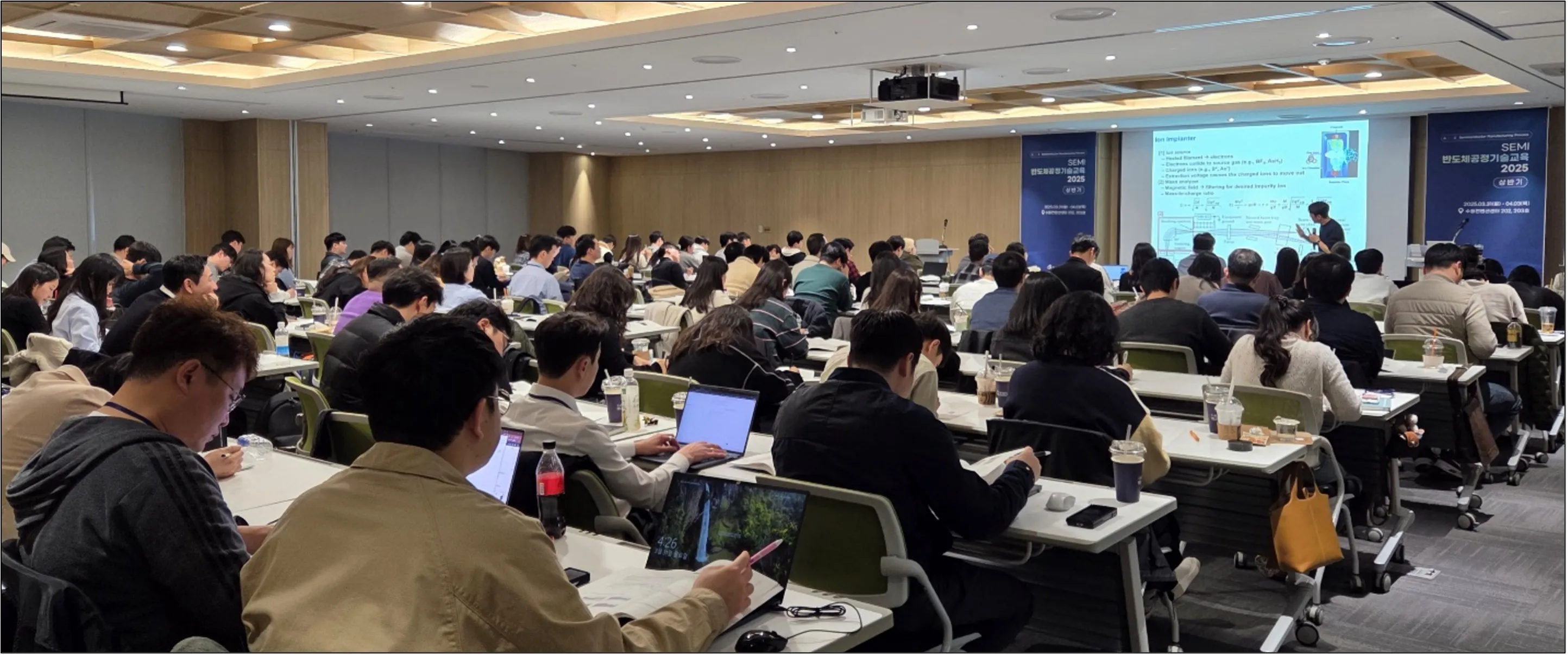
본 강의는 반도체 분야의 기초 이해를 목표로 하며, 크게 세 가지 핵심 주제로 구성되어 있다.

1) 반도체 기술 및 산업의 발전 과정을 살펴보고, 이를 바탕으로 현재 반도체 산업의 동향과 중요성을 이해하는 것을 목표로 한다.
2) 반도체 재료의 특성과 반도체 소자의 기본적인 동작 원리를 정성적인 관점에서 이해하는 것을 목표로 한다.
3) 반도체 소자 및 IC 칩 제작에 필요한 주요 단위공정기술 및 집적공정기술의 기초에 대해 이해하는 것을 목표로 한다.

※ 연사정보

9:00 am - 10:00 am
김장현
김장현
교수
아주대학교

Overview of VLSI Technology

본 강의는 최신 반도체 제조 기술 중 하나인 3나노미터(3nm)급 공정을 기반으로 한 GAA(Gate-All-Around) MOSFET(Metal-Oxide-Semiconductor Field-Effect Transistor) 소자에 대한 구조와 동작 이해를 중점으로 다룹니다. 최근 발표된 연구 기술과 논문을 기반으로 반도체 소자의 연구 동향과 기술적인 이슈를 탐구합니다.

※ 연사정보

10:00 am - 10:10 am

Q&A, Break

10:10 am - 11:10 am
김장현
김장현
교수
아주대학교

Overview of VLSI Technology

11:10 am - 11:25 am

Q&A, Break

11:25 am - 1:00 pm

Lunch

1:00 pm - 2:00 pm
이석배
이석배
프로
SK siltron

Semiconductor Silicon Wafer Preparation

본 강의에서는 Silicon ingot을 성장시키는 growing process와 Wafer의 형상 제어를 목적으로 하는 shaping process, Wafer 표면의 경면을 목적으로 평탄도를 제어하는 Polishing proces, 마지막으로 청정도 제어 목적의 Cleaning process를 포함하는 wafering process 설명을 통해 전반적인 wafer 제조 process에 대한 이해를 높일 예정이다.
또한 Silicon wafer의 metrology 를 Crystal, Surface, Electrical, Contamination 관점에서 설명함으로써 분석 방법 및 영역에 대한 포괄적 이해를 돕고자 한다.

※ 연사정보

2:00 pm - 2:10 pm

Q&A, Break

2:10 pm - 3:10 pm
이석배
이석배
프로
SK siltron

Semiconductor Silicon Wafer Preparation

3:10 pm - 3:25 pm

Q&A, Break

3:25 pm - 4:25 pm
김태성-교수님.jpg
김태성
교수
성균관대학교

CMP & Cleaning

반도체 소자의 고속화 및 고집적화에 따라 다층배선구조에 있어서 배선층수의 증가와 패턴의 미세화에 대한 요구가 여전히 높다. CMP (Chemical Mechanical Planarization)는 미세패턴을 형성하기 위한 노광장치의 Depth of focus가 작아지면서 광역평탄화를 실현하기 위해 도입되었는데, 현재는 STI, Cu damascene 등 패턴형성 및 TSV 같은 packaging 쪽에도 사용되고 있어 그 중요성이 나날이 커지고 있다. Cleaning은 Particle, Metal, Polymer, Organic contamination, Native Oxide 및 Damaged Layer 등과 같은 Wafer 상의 원하지 않는 물질들을 제거하여, Device Yield를 감소시키는 노광 불량, Gate Oxide 불량, 전기적 접촉저항 불량 및 배선의 단락 등과 같은 결함을 제어하는 모든 공정을 의미한다. 패턴 미세화에 따라 난이 도가 급격히 증대되어 패턴손상 없는 새로운 세정공정개발의 필요성이 커지고 있다. 본 강 의에서는 CMP 및 cleaning의 기본 개념과 필수 구성요소를 장비와 재료 측면에서 살펴보고, 차세대 CMP 및 cleaning의 방향에 대해서 다루고자 한다.

※ 연사정보

4:25 pm - 4:35 pm

Q&A, Break

4:35 pm - 5:35 pm
김태성-교수님.jpg
김태성
교수
성균관대학교

CMP & Cleaning

5:35 pm - 5:50 pm

Q&A, Adjourn

9:00 am - 10:00 am
김홍익
김홍익
TL
SK hynix

Lithography

리소그래피(Lithography, 노광 공정)는 반도체 공정에서 회로의 ‘밑그림’을 웨이퍼에 정밀하게 그려 넣는 핵심 단계이다. 설계된 회로 패턴은 스캐너 등의 노광 장비를 통해 웨이퍼 표면에 도포된 감광제(포토레지스트) 위에 빛으로 전사되며, 이 과정의 반복을 통해 실제 반도체 회로를 형성한다. 본 강의에서는 리소그래피 공정의 기본 원리와 역사적 발전, 광원 및 렌즈 시스템, 포토레지스트의 종류와 특성, 노광 장비의 구성과 작동 원리, 그리고 해상도 향상을 위한 최신 기술까지 단계별로 설명한다. 이를 통해 리소그래피 공정의 핵심 개념을 이해하고, 미래 반도체 기술 발전에 필요한 기초 역량을 갖추는 데 기여할 수 있다.

※ 연사정보

10:00 am - 10:10 am

Q&A, Break

10:10 am - 11:10 am
김홍익
김홍익
TL
SK hynix

Lithography

11:10 am - 11:25 am

Q&A, Break

11:25 am - 1:00 pm

Lunch

1:00 pm - 2:00 pm
임한진
임한진
교수
삼성전자 SSIT

Implantation & Diffusion

Doping 및 Diffusion 공정 (Implantation, Annealing, Oxidation, Nitridation, Deposition)은 지난 50 년간 핵심 반도체 제조 기술로서 고성능 소자 제작을 위해 사용되어 왔으며, 현재도 새로운 기술로서 진화하고 있다. 본 중급 과정에서는 각 공정에 대한 기초, 심화, 응용에서부터 차세대 공정까지 폭넓게 다룰 예정이다. Ion implantation 에서는 목적, 장단점, Hardware 구성, Process 응용, Doping profile, Channeling, Defect, TED, 신기술에 대해 소개한다. Annealing 에서는 목적, 종류 (sRTA, fRTP, LSA), Activation, Junction 조절, 장비 종류 및 Hardware 구성에 대해 소개한다. Oxidation 에서는 산화 Kinetics, 산화막 물성, Defect/Charge, 다양한 산화 방식(Dry, Wet, Plasma, Radical)과 장비에 대한 소개가 이루어진다. Nitridation 에서는 방식(Thermal, Plasma)에 따른 N profile, 소자 특성, 장비에 대해 다룬다. Deposition (LPCVD, ALD) 에서는 증착 Kinetics, 분류 방식, 다양한 박막 종류 (Poly Si, SiO2, Si3N4, SiON, Metal) 및 공정 응용에 대해 소개할 예정이다.

※ 연사정보

2:00 pm - 2:10 pm

Q&A, Break

2:10 pm - 3:10 pm
임한진
임한진
교수
삼성전자 SSIT

Implantation & Diffusion

3:10 pm - 3:25 pm

Q&A, Break

3:25 pm - 4:25 pm
박용신 수석.png
박용신
수석
삼성전자

Etch

최근 반도체 집적도가 증가하면서 Patterning 공정에 대한 난이도 역시 급격히 증가하고 있다. 특히 2D 및 3D Patterning을 모두 담당하는 Etching 공정의 중요성은 그 어느 때 보다도 높아진 상황이다. 본 강의에서는 Etching process를 구현하는데 필수적인 Plasma physics 및 engineering을 소개하고, 기본적인 Etching mechanism 및 주요 물질 별 Etching chemistry, 차세대 Etching 기술 트렌드 등을 조망하고자 한다.

※ 연사정보

4:25 pm - 4:35 pm

Q&A, Break

4:35 pm - 5:35 pm
박용신 수석.png
박용신
수석
삼성전자

Etch

5:35 pm - 5:50 pm

Q&A, Adjourn

9:00 am - 10:00 am
강동균
강동균
TL
SK hynix

Thin Film

최근 반도체 산업은 초고속, 저전력, 고집적 등 메모리 소자의 성능을 향상시키기 위한 방향으로 연구 개발을 활발하게 추진하고 있습니다. 반도체 소자를 실제로 구현하고 제품으로 만들어내는 반도체 제조 공정은 이를 위해 새로운 기술 및 소재의 개발과 함께 기존 소자의 구조를 개선하는 등의 다양한 연구를 병행하고 있습니다.
본 강의는 Thin Film 공정의 기본 개념 및 용어와 함께 해당 공정의 증착 방법, 각 증착 물질의 특징과 장단점에 대해 이해하고 이를 바탕으로 특히, Dielectric, Metal 물질 별 응용 사례를 파악하여 Thin Film 공정에 대한 이해도를 높이는 과정입니다.

※ 연사정보

10:00 am - 10:10 am

Q&A, Break

10:10 am - 11:10 am
강동균
강동균
TL
SK hynix

Thin Film

11:10 am - 11:25 am

Q&A, Break

11:25 am - 1:00 pm

Lunch

1:00 pm - 2:00 pm
7.SPT2022(2H)_SK하이닉스 오재형 TL_사진.jpg
오재형
TL
SK hynix

Metrology & Inspection

반도체 회로 패턴이 점점 미세화 되면서 반도체 소자를 형성하기 위한 공정 진행 방법 또한 점점 어려워지고 복잡해지고 있다. 특히 반도체 제품의 Pattern Shrinkage, SPT/DPT 공정의 확대, 구조변화 등에 따라 다양한 형태의 불량들이 발생할 뿐만 아니라 불량 Size 또한 더욱더 작아지고 있어 제조 공정 과정에서 발생되는 문제점을 빠르고 정확하게 확인할 수 있는 In-line 계측 기술에 대한 요구가 높아지고 있다. 본 강의에서는 반도체 제조 공정 과정에서 사용되는 Metrology & Inspection 분야의 중요 장치들의 기본적인 작동 원리와 종류를 알아보고, 각 장비들의 활용 사례를 통하여 공정상의 문제점 파악과 해결 방법들을 살펴보고, 향후 신제품 대응에 필요한 차세대 Metrology & Inspection Tools의 개발 Trend에 대해서 다루고자 한다.

※ 연사정보

2:00 pm - 2:10 pm

Q&A, Break

2:10 pm - 3:10 pm
7.SPT2022(2H)_SK하이닉스 오재형 TL_사진.jpg
오재형
TL
SK hynix

Metrology & Inspection

3:10 pm - 3:25 pm

Q&A, Break

3:25 pm - 4:25 pm
김종훈
김종훈
TL
SK hynix

Packaging

반도체 패키지란 일반적으로 전공정에서 실리콘에 형성된 회로를 외부로 연결해주고 보호해줄 수 있도록 하는 후공정 단계이다. 반도체가 발전 할수록 더욱 빠르게 동작하고, 다양한 분야에 활용함으로 인해 열방출에 대한 성능과 고 신뢰성을 요구하게 되었다. 최근 AI의 성장을 위해서는 패키지의 발전도 같이 이루어져야 한다는 목소리가 커지고 있다. 이제는 패키지가 외부로 전기적, 기계적 연결하고 열방출, 반도체의 보호에 대한 역할 뿐만 아니라 반도체 회로 소형화의 한계로 패키지에 고속화, 다기능화, 저전력 등의 기능을 요구 하고 있다. 이에 발맞추어 실리콘 관통 적극을 이용하여 HBM(High Band width) 메모리가 등장하고 있으며 이종 칩을 연결하여 새로운 시스템 인 패키지가 만들어지고 있기도 하다. 점점 패키지의 역할이 중요해지고 있는 시점에 맞추어 본 강의에서는 반도체 패키지가 어떤 역할을 하는지 앞으로의 Trend를 소개하고, Substrate를 이용한 일반적인 반도체 패키지 공정과 새로운 시장을 위해 적용되고 있는 flip chip 및 웨이퍼 레벨 패키지 기술 실리콘 관통 전극(TSV)를 이용한 3D 적층 패키지 기술과 이종 칩 연결 기술에 대해 소개하고자 한다.

※ 연사정보

4:25 pm - 4:35 pm

Q&A, Break

4:35 pm - 5:35 pm
김종훈
김종훈
TL
SK hynix

Packaging

5:35 pm - 5:50 pm

Q&A, Adjourn

- Workforce Development

SEMI 반도체공정기술교육은 반도체 장비 및 재료 분야 종사자들이 반도체 제조공정을 깊이 이해하고, 업무를 원활히 수행할 수 있도록 지원합니다. 이 교육은 반도체 장비 및 재료 제조에 종사하는 엔지니어, 기획 및 마케팅 실무자, 제조업체 기술영업사원, 이공계 학생을 대상으로 합니다. 웨이퍼 제조부터 공정 결함을 측정/계측하는 MI기술까지, 반도체 칩 제조공정을 한눈에 볼 수 있는 기회를 제공하오니 많은 관심과 참여를 부탁드립니다.
Off Add to Calendar 2026-04-20 00:00:00 2026-04-23 00:00:00 SEMI 반도체공정기술교육 2026 (상반기) SEMI 반도체공정기술교육은 반도체 장비 및 재료 분야 종사자들이 반도체 제조공정을 깊이 이해하고, 업무를 원활히 수행할 수 있도록 지원합니다. 이 교육은 반도체 장비 및 재료 제조에 종사하는 엔지니어, 기획 및 마케팅 실무자, 제조업체 기술영업사원, 이공계 학생을 대상으로 합니다. 웨이퍼 제조부터 공정 결함을 측정/계측하는 MI기술까지, 반도체 칩 제조공정을 한눈에 볼 수 있는 기회를 제공하오니 많은 관심과 참여를 부탁드립니다. 대한민국 수원컨벤션센터 SEMI.org [email protected] Asia/Seoul public Asia/Seoul 등록 바로가기
Event format
Promote in calendar
Off


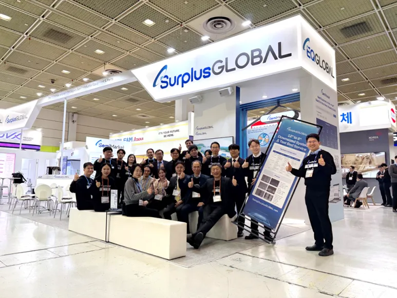
서플러스글로벌이 국내 최대 반도체 산업 전시회 ‘세미콘 코리아(SEMICON KOREA) 2026’ 참가를 계기로 자사 B2B 플랫폼 ‘세미마켓(SemiMarket)’의 사용자 기반을 대폭 확대했다. ​ 
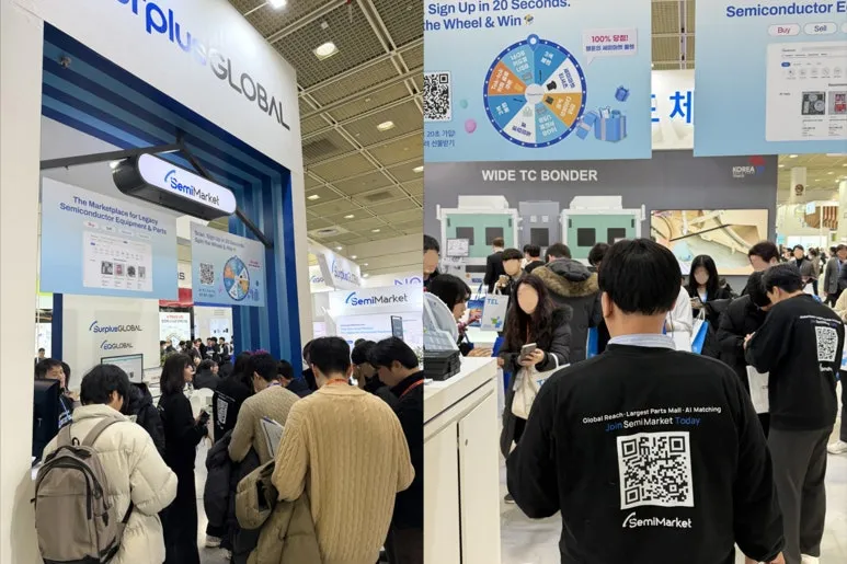
지난 2월 11일부터 13일까지 서울 코엑스에서 열린 ‘세미콘 코리아 2026’에서 약 3000명의 업계 관계자가 서플러스글로벌 부스를 찾았으며, 이 중 800명 이상이 현장에서 세미마켓 회원으로 가입했다. 단기간 내 이뤄진 대규모 사용자 유입은 레거시(성숙공정) 장비·부품 거래의 디지털 전환 수요가 확대되고 있음을 보여주는 지표로 해석된다. ​ 

특히 가입자 중에는 글로벌 반도체 장비사 임직원과 공정·유지보수 엔지니어들이 다수 포함된 것으로 나타났다. 실제 장비 운용과 구매 의사결정에 관여하는 실무 인력들이 플랫폼에 직접 참여했다는 점에서 세미마켓의 실질적 활용 가능성을 현장에서 확인했다는 평가다. ​  ​ 


오프라인 전시를 계기로 온라인 플랫폼 유입 역시 동반 확대되는 모습이다. 지난해 6월 오픈 직후 일평균 방문자 수가 1500명 수준이었으나 최근 두 달 사이 4000명 수준으로 증가했다. 회사 측은 실제 장비·부품 실수요자 유입이 늘어나고 있다며, 연내 플랫폼 트래픽을 단계적으로 확대해 일평균 2만 명 수준까지 성장시키는 것을 목표로 하고 있다고 밝혔다. ​

 또한 세미마켓 가입 회원들은 신규 등록되는 레거시 반도체 장비·부품 정보와 수요 기반 추천 정보를 정기적으로 받아볼 수 있다. 회사 측은 광고성 홍보가 아닌 실시간 매물 동향과 시장 흐름을 반영한 데이터 기반 정보를 개인화해 제공하는 데 초점을 두고 있다고 밝혔다. ​ 

김정웅 서플러스글로벌 대표는 “전시 현장에서 확인한 상담 및 가입 흐름을 종합해 볼 때 올 하반기 레거시 반도체 장비 및 부품의 글로벌 수요는 점진적인 회복세를 보일 것”이라며 “세미마켓을 중심으로 글로벌 거래 참여자를 지속 확대해 나가겠다”고 말했다. ​ 한편 서플러스글로벌은 오는 3월 25일부터 27일까지 중국 상하이에서 열리는 ‘세미콘 차이나(SEMICON CHINA) 2026’ 전시회 참가를 준비 중이다.