Registration

※ 사전등록 일정: 2026년 5월 14일(목) ~ 6월 17일(수) 오후 5시
Registration Fee
- Early Bird
- SEMI 회원사: KRW 180,000
- 비회원사: KRW 240,000
- On site
- SEMI 회원사: KRW 300,000
- 비회원사: KRW 300,000
※ 상기 등록비는 부가세가 포함된 가격입니다.
OVERVIEW
- 일시: 2026년 6월 23일(화) 12:30-17:00
- 장소: 수원컨벤션센터 2층 202호
- 언어: 한국어/영어 (동시통역 제공)
NOTICE
- 아젠다는 연사 사정에 의하여 임의로 변경될 수 있습니다.
- 발표자료는 연사의 배포 동의를 얻은 자료에 한하여 행사 종료 후 SEMI Korea 프로그램 등록사이트(https://semikrprogram.com)에 로그인하셔서 다운로드하실 수 있습니다.
- 주차비는 제공되지 않습니다.
CONTACT
- SEMI Korea 프로그램팀 ([email protected])
대한민국
수원컨벤션센터
Networking Reception

Opening

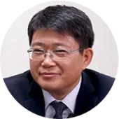
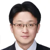
Restructuring of the Semiconductor Industry Driven by AI and the Opportunities It Creates
The rapid expansion of AI is fundamentally reshaping the semiconductor industry, driving unprecedented investment in AI data centers, accelerating technological transitions, and redefining competitive dynamics across the ecosystem. At the same time, growing debates around the sustainability of AI-related investments and the potential risks of an AI bubble are creating new uncertainties for industry players.
Changwook Kim, Managing Director and Partner at BCG and leader of the semiconductor practice in Korea, will present on the “AI-Driven Restructuring of the Semiconductor Industry and the Opportunities it creates.” The session will cover AI data center investment trends and outlook, the impact of AI on the memory semiconductor market, recent changes across the semiconductor ecosystem including fabless, foundry, packaging, and memory technologies, and the strategic implications and opportunities for semiconductor companies.
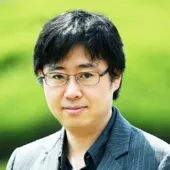
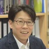
Beyond Scaling: Building the Next-Generation AI Semiconductor Framework
AI is moving from large-scale model training toward inference and agent-based services. GPUs, HBM, and 2.5D interconnects have powered the first wave of AI acceleration, but the future is diversifying—bringing AI accelerators, CPUs, general-purpose memory, and on-die AI semiconductors into play. From a memory-centric view, the demand for massive capacity, ultra-fast speed, and wide I/O bandwidth is clear. Yet the most urgent challenge is low power. This talk will explore the current limits of DRAM core die technology in HBM and highlight new device structures designed to break through these bottlenecks. We will look at the shift beyond the traditional 1T1C DRAM cell toward oxide-semiconductor-based 2T0C architectures, advances in bonding methods, and the potential of glass substrates. We will also examine strategies for achieving low-power operation—from smarter architectures to heterogeneous integration of processors and memory—and discuss how these innovations open opportunities across devices, materials, equipment, and packaging. By framing these breakthroughs within a broader AI semiconductor technology framework, the session will provide a clear view of both the technical challenges and the strategic directions shaping the next era of global semiconductor innovation.
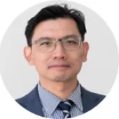
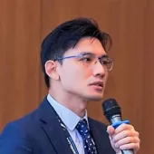
AI Demand Meets Capacity Reality: Semiconductor Infrastructure and Korea’s Role in the Next Investment Cycle
AI is reshaping the semiconductor industry from both the demand side and the infrastructure side. While AI accelerators, HBM, advanced logic, and data-center infrastructure continue to drive strong growth, the broader market remains uneven, with consumer-driven segments recovering more gradually and macro uncertainty still shaping investment decisions. This presentation will review the key market forces behind the current semiconductor cycle and examine how AI demand is translating into fab investment, capacity expansion, and equipment spending.
The discussion will highlight SEMI’s latest view of global fab investment, capacity growth, and regional expansion. It will also address why the next phase of growth depends not only on headline demand, but also on qualified capacity, technology migration, packaging and test readiness. With Korea’s leadership in memory and manufacturing execution, the presentation will place Korea’s role within the broader global infrastructure buildout supporting the AI era.
Break

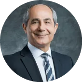
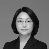
Packaging as the New Strategic Layer
As monolithic scaling approaches the physical and economic limits of Moore’s Law, Advanced Semiconductor Packaging (ASP) has transitioned from a routine backend process to the primary driver of microelectronic innovation. Driven by an unprecedented surge in demand for Artificial Intelligence (AI), high-performance computing (HPC), and 5G infrastructure, ASP has emerged as the new strategic layer in the global technology ecosystem, reshaping hardware architecture and market competition.
Through heterogeneous integration, advanced packaging techniques—such as 2.5D/3D stacking and fan-out wafer-level packaging—bypass single-die fabrication constraints. By combining disparate, optimized chiplets into a unified system, ASP fulfills the skyrocketing commercial need for massive interconnect densities, ultra-low latencies, and extreme thermal efficiencies.
Ultimately, semiconductor leadership is no longer defined solely by front-end lithography nodes, but by the ability to architect complex, multi-die systems. Packaging has effectively become the critical differentiator, supply chain constraint, and the ultimate bottleneck for future technological supremacy.
Panel Discussion
Closing
반도체 산업은 이제 기술적 진보를 넘어, 글로벌 정치와 AI가 주도하는 복잡한 거시적 변화에 직면해 있습니다. Global Semiconductor Market Insight Forum은 이러한 환경 변화 속에서 반도체 생태계를 이끄는 주요 리더들이 모여, 산업을 견인하는 기술과 시장의 동인을 살펴보고 산업 투자 흐름에 대한 이해를 높일 수 있도록 마련한 포럼입니다.
특히 패널 디스커션을 통해 각기 다른 기술·시장·투자 관점에서 바라본 반도체 산업에 대한 인사이트를 공유함으로써, 단일 시각을 넘어 보다 입체적인 전략적 통찰을 제공할 예정입니다. 이를 통해 산업의 미래를 고민하는 C‑레벨 리더들이 한자리에 모여, 반도체 산업의 중장기 방향성과 비전에 대한 공감대를 형성할 수 있기를 기대합니다.