downloadGroupGroupnoun_press release_995423_000000 copyGroupnoun_Feed_96767_000000Group 19noun_pictures_1817522_000000Member company iconResource item iconStore item iconGroup 19Group 19noun_Photo_2085192_000000 Copynoun_presentation_2096081_000000Group 19Group Copy 7noun_webinar_692730_000000Path
Skip to main content
Default Banner Image

Business

United States Register Pulsus webinar Business Technical Featured Speakers
Highlighted content

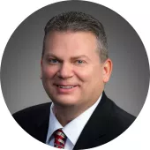
Arjen Janssens, Senior Director PLD, Lam Research Corporation


Arjen Janssens initially worked on Pulsed Laser Deposition (PLD) during his Master’s Degree in Applied Physics at the University of Twente in 2001, and then during his internship at Stanford University on superconducting thin films.


Arjen started his career as a strategic consultant at Arthur D. Little, and after a year become a shareholder and consultant of Quintel Management Consultancy (spin-out of Arthur D. Little). In 2004 he started studying for his PhD. at the University of Twente, focusing on depositing Piezo materials with PLD. During his PhD, he completed the Executive MBA at TSM Business School of Technology, and co-founded Solmates. Currently Arjen is Senior Director PLD at Lam Research and is very proud of how the PLD technology has matured into a high-volume production system at Lam.

United States

arjen janssens
Dr. Arjen Janssens
MSIG

And yes, we’ve got a solution for that.

MEMS devices have become well established as critical components in a wide range of everyday applications. Accelerometers and gyroscopes improve safety in automotive applications, RF filters enable wireless connectivity in mobile phones, and MEMS microphones are at the heart of voice control technologies that connect us to an ever-increasing range of smart, consumer products.

Developers are now looking to the next generation of MEMS devices that will enable new applications and improve the performance of existing solutions. Capacitive based MEMS devices have proven to be highly successful, but after significant improvements of both design and manufacturing it is becoming increasingly difficult to improve their performance. To overcome this challenge, designers are looking to Piezoelectric based MEMS devices that can offer a paradigm shift in capability.

In this webinar, discover Lam Research’s solution a pioneering approach to thin film deposition.
8:00 am - 9:00 am Off Add to Calendar 2024-03-27 08:00:00 2024-03-27 09:00:00 Enabling PiezoMEMS applications for today and tomorrow And yes, we’ve got a solution for that.MEMS devices have become well established as critical components in a wide range of everyday applications. Accelerometers and gyroscopes improve safety in automotive applications, RF filters enable wireless connectivity in mobile phones, and MEMS microphones are at the heart of voice control technologies that connect us to an ever-increasing range of smart, consumer products.Developers are now looking to the next generation of MEMS devices that will enable new applications and improve the performance of existing solutions. Capacitive based MEMS devices have proven to be highly successful, but after significant improvements of both design and manufacturing it is becoming increasingly difficult to improve their performance. To overcome this challenge, designers are looking to Piezoelectric based MEMS devices that can offer a paradigm shift in capability.In this webinar, discover Lam Research’s solution– a pioneering approach to thin film deposition. United States SEMI.org [email protected] America/Los_Angeles public

Event format

Registration

Member: $49
Non-Member: $99

Registrants will receive the presentation recording and PDFs of Webinar #3.

Taylor Zhao
Manager, Programs & Committees
[email protected]

+
United States Register Now Business Technical

SiC—Silicon Carbide Webinar #3: Bidirectional SiC and GaN Switch Technology

There are numerous mass volume power applications where it is necessary to control the flow of bidirectional power, including electric vehicles (vehicle to grid, vehicle to home, and vehicle to vehicle), distributed and grid-tie power systems using regenerated energy and/or energy storage components, and solid-state circuit breaker protection. Silicon carbide (SiC) and gallium nitride (GaN) based bidirectional power switches can enable these applications with their compelling advantages of high efficiency, high blocking voltage capability, and low system weight and volume.  In particular, monolithic switches that allow for bidirectional symmetric conduction and voltage blocking with a chip area close to that of a similarly rated unidirectional switch are ideally suited to fuel a revolution in power electronics technology. Today, monolithic bidirectional (MBD) power semiconductor switches are not commercially available. Instead, back-to-back (anti-series) connection schemes of unidirectional power MOSFETs or IGBTs are typically used, resulting in a 4X penalty in chip area and high cost. However, various types of SiC and GaN bidirectional concepts are being investigated including bonded-wafer bidirectional IGBTs, monolithic dual-gate bidirectional GaN switches, and monolithic back-to-back connected SiC MOSFETs and JFETs.

In this presentation, the semiconductor technology of SiC and GaN bidirectional switches will be reviewed including their operating principles, and their lateral and vertical geometry configurations. The performance advantages of MBD switches will be highlighted. Promising MBD devices reported to date will be analyzed, and the key bidirectional switch applications of solid-state circuit breakers and current-source-inverters will be discussed. As SiC and GaN devices approach mass commercialization propelled by insertion in electric vehicles and consumer electronics, respectively, fabrication of SiC/GaN MBD switches is becoming economically viable enabling their wide adoption in key volume applications. 


View other webinars in the SiC Series

  • Webinar #1—Silicon Carbide Material Properties, Key Applications, and Fabrication Basics: Making the Transition from Silicon
  • Webinar #2—Non-CMOS Compatible SiC Power Device Fabrication in Volume Si Fabs
  • Webinar #3—Bidirectional SiC and GaN Switch Technology 
  • Webinar #4—Understanding SiC Chip Cost, the Impact of Defects, and the Case of Price Parity with Si at the System Level 
  • Webinar #5—SiC Edge Termination Technology


Meet the Speaker

Biography

United States

Victor Veliadis, PowerAmerica
Victor Veliadis, PhD
Executive Director and Chief Technology Officer,
PowerAmerica

Now Available On-Demand!

Join us online for the third webinar in the Silicon Carbide Series as we review the semiconductor technology of SiC and GaN bidrectional switches, analyze promising MBD devices, and discuss the key bidrectional switch applications of solid-state circuit breakers and current-source-inverters. 

9:00 am - 10:00 am Off Add to Calendar Disabled America/Los_Angeles 1
Event format

For general questions and inquiries, please contact [email protected]

+
United States 360x317_Event_Calendar_Ad_SUOverviewSemiconductors_v2@2x Business Technical
Highlighted content

Updated time:

Day 1: 8:30 am - 5:30 pm PT
Day 2: 8:30 am - 12:30 pm PT

Registration will be closed at 12:00am on May 7.

Learning Objectives:

  • Gain a comprehensive understanding of the semiconductor industry and the manufacturing process, design and eco-system of the semiconductor industry and understand the jargon, tools, and materials used in the design and fabrication of an IC
  • Effectively be able to communicate semiconductor manufacturing concepts with other associates and industry professionals

Who Should Attend:

  • New personnel entering the field
  • Any one wanting an understanding of semiconductor manufacturing

Course Topics:

  • Basic electronics and microelectronics terms and definitions
  • Microelectronics and the role of integrated circuits
  • Define process nodes : explanation of process nodes and how they relate to device performance and cost
  • Device physics and transistor operation: understanding of the physical principles behind device operation and the functioning of transistors
  • Crystal growth and wafer prep: overview of crystal growth techniques used in semiconductor manufacturing
  • Explanation of wafer preparation techniques and materials used
  • FDSOI, fin fets, gate all around (GAA) transistors
  • Circuit design and layout
  • Mask making techniques and materials used in lithography
  • Clean rooms
  • Lithographic techniques
  • Plasma etch, wet etch and cleaning processes
  • Ion implantation
  • Diffusion techniques
  • RTP, CVD, ALD, ALE techniques and their impact on device performance
  • Electro-plating, sputtering
  • Testing
  • Wire bonding
  • Packaging techniques
  • Metrology tools and applications
  • The major players in the semiconductor ecosystem

Instructor:

Denny headshot

Denny Frye 

Course Instructor

PT International, LLC

Biography


SEMI Headquarters
673 S Milpitas Blvd
Milpitas, CA 95035
United States

- Workforce Development

The purpose of this course will provide a comprehensive understanding of the semiconductor industry and the manufacturing process of an integrated circuit (IC). The course is designed for new personnel entering the field or individuals who are looking for a well-rounded understanding of all the jargon, tools, and materials used in the IC manufacturing process.

Limited time offer!

  • Members: $1295 $1195
  • Non-members: $1495 $1395
  • Students/Veterans: $1195 $1095

* For group orders with 10+ attendees, and for Students/Veterans discounted pricing, please contact [email protected]
* Coffee, refreshments, and lunch will be provided for all attendees, ensuring a satisfying and energizing experience throughout the day.

Off Add to Calendar 2024-05-08 00:00:00 2024-05-09 00:00:00 Overview of Semiconductor Manufacturing The purpose of this course will provide a comprehensive understanding of the semiconductor industry and the manufacturing process of an integrated circuit (IC). The course is designed for new personnel entering the field or individuals who are looking for a well-rounded understanding of all the jargon, tools, and materials used in the IC manufacturing process.Limited time offer!Members: $1295 $1195Non-members: $1495 $1395Students/Veterans: $1195 $1095* For group orders with 10+ attendees, and for Students/Veterans discounted pricing, please contact [email protected]* Coffee, refreshments, and lunch will be provided for all attendees, ensuring a satisfying and energizing experience throughout the day. SEMI Headquarters 673 S Milpitas Blvd Milpitas, CA 95035 United States SEMI.org [email protected] America/Los_Angeles public Register Today
Belgium France Germany Ireland Italy Japan Malaysia Singapore South Korea Taiwan United States Vietnam 360x317_Event_Calendar_Ad_SURoadmap_v6@2x (1).png Business Featured Speakers
Highlighted content

SEMI University celebrates its first anniversary! Our pledge remains unwavering: providing comprehensive, technical education to equip you with the skills needed for a prosperous journey in the semiconductor sector.

Are you ready to take your semiconductor industry knowledge to the next level? We're thrilled to invite you to our upcoming webinar titled "SEMI University - Introduction and 2024 Roadmap." This webinar promises to be an informative session where you'll gain insights into the latest updates, exciting live trainings, new certifications, and courses offered by SEMI U in 2024.  

During this webinar, you can expect to:  

  • Discover the latest updates and enhancements to SEMI U's course catalog.  
  • Learn about the exciting live, in-person training courses scheduled for spring of 2024.  
  • Get insights into new certifications and courses designed to keep you ahead in the industry.  
  • Gain access to a special 10% discount on ALL courses.  

Choose your session:

United States

Naresh Naik
Naresh Naik
Director, SEMI University
SEMI
Workforce Development

Join us to discover our current course offerings, upcoming additions, new certifications, and more! Engage in a Q&A session. Plus, by attending this free webinar, you'll receive a 10% discount code for all our courses.

Off Add to Calendar 2024-03-19 00:00:00 2024-03-19 00:00:00 SEMI University - Introduction and 2024 Roadmap Join us to discover our current course offerings, upcoming additions, new certifications, and more! Engage in a Q&A session. Plus, by attending this free webinar, you'll receive a 10% discount code for all our courses. United States SEMI.org [email protected] America/Los_Angeles public

Event format

Registration

SEMI Members:  $49

Use your corporate email address during log in to be recognized as a SEMI Member.

Non-Members:  $75

Students:  Free

Contact [email protected] with a picture of your student ID to receive your discount code.

Belgium France Germany Ireland Italy United States FEMC 17 Tile Recorded Business Executive Featured Speakers
Highlighted content

Bio

The healthcare industry has transformed over the last twenty-five years due to the co-development of diagnostics along with state-of-the-art therapeutics and treatments; notably, this has led to the field of companion diagnostics. The best example of this is the prescribed use of insulin based on glucose levels monitored via test strips or the continuous glucose monitor. The future goal of medicine is to have truly personalized treatment protocols based on an individual’s biometrics, physiology, and exposure.  

However, this goal requires further identification and quantitation of biomarkers and health exposures, both biological and chemical, both at the point-of-care as well as in real-time.  Therefore, technologies are needed that can miniaturize current diagnostics to make them inexpensive, simple-to-use, and ideally wearable. 

However, where and what to sense remains a critical question to solve, as each biofluid, including blood, sweat, saliva, tears, breath, and exhaled breath condensate contains a different profile of biomarkers. Additionally, biomarkers have vastly different physiochemical properties and abundances, which present different challenges as well as require a range of sensing modalities.  Therefore, this course will be an overview of the “What, Where, and How of Sensing to Meet Current and Future MedTech Needs”.  At the end of the course, a perspective of where these technologies can impact the future of health outcomes will be presented as well as key considerations for future technologies to gain commercial acceptance

ABOUT THE SPEAKER

Dr. Michael Brothers, PMP currently is a Principal Scientist and Technical Program Manager at UES, a Blue Halo Company. In these roles, Dr. Brothers supervises contractors executing research to identify biomarkers indicative of human performance, develop novel sensors, as well as field research. Dr. Brothers also serves as a subject matter expert on biochemical sensors, both in the liquid phase and gas phase, for the 711th Human Performance Wing at Wright Patterson Air Force Base. 

Notably, Dr. Brothers has co-authored multiple publications and patents on using novel sensing modalities to sense in complex fluids and environments, including jet fuel, sweat, saliva, and breath. Dr. Brothers has also served as the Principal Investigator on sensor development efforts for both optical based gas sensors and flexible, ink-printed gas sensors for wearable applications.  

Dr. Brothers has his Ph.D. from the University of Illinois Urbana-Champaign in Chemical Biology and his B.S. in Chemistry and Biology from the University of Cincinnati.  
 

United States

Dr. Michael Brothers
Principal Scientist and Technical Program Manager
UES, a Blue Halo Company
Gity Samadi
Dr. Gity Samadi
Director, R&D Programs
SEMI
FlexTech

This webinar featured Dr. Michael Brothers of UES, a Blue Halo Company, outlining the status of personalized medical treatment protocols based on an individual’s biometrics, physiology, and exposure. This course will be an overview of the “What, Where, and How of Sensing to Meet Current and Future MedTech Needs"

10:00 am - 12:00 pm Off Add to Calendar Disabled America/Los_Angeles Watch Now
Event format
Promote in calendar
Off

Registration Details

Registration is free of charge, but must be done in advance 


Belgium France Germany United States Register Now Business Technical

UCLA
Los Angeles, CA
United States

1:00 pm - 3:00 pm

Phase 2 Project Introductions

- Low-SWaP-C, GPS-free PNT technology
- Novel materials, fabrication & packaging techniques and approaches
- Advancements in atomic clock and quantum sensor photonics

3:00 pm - 4:30 pm

Break Out Sessions

Thrust Area 1: Novel Materials, Fabrication, and Packaging Techniques for Low-SWaP Inertial and PNT Sensors
Thrust Area 2: Advanced Active and Passive Integrated Photonics for Low-SWaP Atomic Clocks, Quantum Systems, & PNT Sensors
Thrust Area 3: Advancements Towards Low-SWaP, GPS-Free PNT Technologies

4:30 pm - 5:00 pm

Group Reports & Wrap Up

MSIG
SEMI MSIG has another $5M in R&D funding for sensor positioning, navigation, and timing (PNT) technology development! Register now to attend our half-day Gap Analysis workshop, taking place April 30, the afternoon before our premier sensor technology-event, the MEMS & Sensors Technical Congress (MSTC). Meet US Gov’t subject matter experts (SME’s) to discuss PNT pain points and get insights into this year’s request for proposals (RFP).
 
The workshop will feature presentations from the new 2024 PNT projects and identify areas for this year’s RFP.
 
Have your voice heard, as SEMI MSIG and the Army Research Lab work to fund PNT R&D technology improvements in a 5-year (2022-2027) $25M program. This gap analysis workshop is a critical component of the program’s 2nd year activities.
1:00 pm - 5:00 pm Off Add to Calendar Disabled America/Los_Angeles

Hotel

Cambridge hotels are expensive in late May, so we have made a deal for you, click here!

We have a room block reserved at DoubleTree Suites by Hilton Hotel Boston, Cambridge for May 21, 2023 through May 25, 2023. Booking your room is simple, just select "Book a Room" to receive your group's preferred rate. Must book rooms before May 12th to obtain discounted rate.

Please book your hotel reservations online for MSTC 2023 Conference or guests can call our 24-7 reservations desk to book your room or please ask for the Front Desk and then provide the Group Code: MSTC 

Book a Room Here

*must book rooms before May 12th to obtain discount rate. 

United States Arizona Chapter Forum Thumbnail Business Executive

Become a Sponsor

Sponsorships can be tailored to meet your branding and marketing objectives. Become a sponsor and brand your company at the Midwest Breakfast Forum.

Contact Lin Tso, [email protected] to learn about available sponsorship opportunities.


Organized by the SEMI Arizona Chapter — 

Join us for the Arizona Chapter Breakfast Forum to explore the thriving innovation ecosystem in the Silicon Desert. 

Is Silicon Desert the New Innovation Hub?


With the influx of high-tech companies and substantial government funding through the CHIPS Act, Arizona has invested over $65 billion in the semiconductor sector emerging as the top destination for semiconductor jobs, investments, and ecosystem expansion in the United States.

Arizona promises to play a leading role in the future of U.S. chip manufacturing and innovation, this has led to the question, is the Silicon Desert the new technology hub?

To maximize opportunities under the CHIPS Act, Arizona has launched an unprecedented collaborative effort, bringing together stakeholders from state and local governments, industry, trade groups, economic development organizations, universities and community colleges, workforce partners, and more.

Get first-hand insight on—

  • Market Trends & Technology Drivers, Emerging Sectors, Forecast and Outlook
  • Semiconductor Growth and How It Will Impact Silicon Desert
  • University and State Infrastructure and R&D
  • Empowering a Sustainable Future in Semiconductor Manufacturing
  • Training the Workforce

These informative sessions will equip you with a comprehensive understanding of Silicon Desert's potential as an innovation powerhouse, the opportunity to network with industry leaders, and foster collaboration with like-minded professionals.

Register now and be a part of this exciting journey shaping the future of technology in the Silicon Desert.

In-Person + Virtual
EMD Electronics
8555 S River Pkwy
Tempe, AZ 85284
United States

Wednesday, May 1, 2024 | Mountain Time

7:30 am - 8:00 am

Check-In and Breakfast

EMD Electronics
8:00 am - 8:05 am
Joe Stockunas, SEMI Americas
Joe Stockunas
President
SEMI Americas

Welcome Remarks

8:05 am - 8:10 am
Kate Dei Cas, EMD Electronics
Kate Dei Cas
Executive Vice President, Global head of Delivery Systems & Services
EMD Electronics, a business of Merck KGaA, Darmstadt, Germany

Welcome Remarks

8:10 am - 8:35 am
Kevin Gorman, EMD Electronics
Kevin Gorman
Senior Vice President & Head of Patterning Solutions
EMD Electronics, a business of Merck KGaA, Darmstadt, Germany

Keynote

8:35 am - 9:00 am
Cori Masters, GARTNER
Cori Masters
Sr. Director Research Analyst, Semiconductor/High Tech Supply Chain
Gartner
9:00 am - 9:25 am
Sean Fogarty, Greater Phoenix Economic Council
Sean Fogarty
Vice President, International Business Development
Greater Phoenix Economic Council
9:25 am - 9:45 am

Break

9:45 am - 9:55 am
Karla Moran, Arizona Public Service
Karla Moran
Manager of Economic Development
Salt River Project (SRP)
9:55 am - 10:05 am
Kelly Patton, Arizona Public Service
Kelly Patton
Economic Development Manager
Arizona Public Service (APS)
10:05 am - 10:25 am
Spencer Wall, DSV Inventory Management Solutions
Spencer Wall
Vice President, Business Development
DSV Inventory Management Solutions

Transforming Your Supply Chain From a Cost Center to a Competitive Advantage

11:30 am
Joe Stockunas, SEMI Americas
Joe Stockunas
President
SEMI Americas

Closing Remarks

SEMI Breakfast Forum Organized by SEMI Arizona Chapter

In-Person + Virtual | Mountain Time


We are sold out!

Thank you for your support. We are excited to welcome you to an outstanding event with excellent speaker lineup and attendees. 

7:30 am - 11:45 am Off Add to Calendar 2024-05-01 07:30:00 2024-05-01 11:45:00 SEMI Arizona Chapter Breakfast Forum—Is Silicon Desert the New Innovation Hub? SEMI Breakfast Forum Organized by SEMI Arizona ChapterIn-Person + Virtual | Mountain TimeWe are sold out!Thank you for your support. We are excited to welcome you to an outstanding event with excellent speaker lineup and attendees.  In-Person + Virtual EMD Electronics 8555 S River Pkwy Tempe, AZ 85284 United States SEMI.org [email protected] America/Phoenix public America/Phoenix 2

Registration

Early Bird (Before April 11, 2024):

Member: $75 | Non-member: $100

Regular:

Member: $100 | Non-member: $125

Registration is final. No refunds provided. No substitutions.

Lin Tso
Email: [email protected]
Phone: +1.408.943.7920

+
United States Register Now Pacific Northwest Chapter Forum Thumbnail Business Executive
Analog Devices Logo 170x65
ASNA 170x65
Mackenzie Corbin Logos
Lighthouse_PNW Sponsor
MWH Constructors Inc. Logo 170x65

Become a Sponsor

Sponsorships can be tailored to meet your branding and marketing objectives. Become a sponsor and brand your company at the Midwest Breakfast Forum.

Contact Lin Tso, [email protected] to learn about available sponsorship opportunities.

AI Driving Fabs of the Future...People, Technology, Infrastructure

There has never been a more exciting time in the history of semiconductor manufacturing. Following the supply chain disruption of the early 2020s, teams rushing to expand operations and add capacity are looking to maximize operating leverage amidst a challenging market backdrop. With dozens of new fully automated 300mm fabs set to open their doors in the next two years, here are the burning questions—

  • What does it mean for the existing 200mm legacy fabs? 
  • What challenges will we face in 2024?
  • How can we solve them together? 

Learn about current market trends, workforce development, equipment advancements, and AI's potential uses in manufacturing. 
Join the conversation on—

  • KEYNOTE: The 5th Industrial Revolution: The Adjacent Possible of AI in Semiconductor Manufacturing—Analog Devices
  • Macro Trends and Value Creation in the Semiconductor Industry—McKinsey & Company
  • What Does It Mean for the Existing 200mm Legacy Fabs?—Microchip Technology
  • AI Use Cases in the Fab—Applied Materials
  • SEMI Smart Manufacturing Initiative—Microchip Technology
  • EXECUTIVE PANEL: Discussion for Talent Acquisition, Workforce Development, Labor Shortage

The SEMI Pacific Northwest Breakfast Forum is a great way to network with colleagues while meeting other local industry leaders.
 

Analog Devices—ADI
14320 SW Jenkins Road
Beaverton, OR 97005
United States

Pacific Time | Thursday, April 25, 2024 | In-Person + Virtual

8:00 am - 8:30 am

Check-In and Networking Breakfast

Analog Devices Logo 170x65
8:30 am - 8:32 am
Joe Stockunas, SEMI Americas
Joe Stockunas
President
SEMI Americas

Welcome Remarks

8:32 am - 8:35 am
Matt Kleinke, Siltronic
Matt Kleinke
Co-Chair of SEMI Pacific Northwest Chapter and Vice President Sales, Americas
Siltronic Corporation
Ian Anderson, Mortenson and PNW Chapter Co-chair
Ian Anderson
Co-Chair of SEMI Pacific Northwest Chapter and Assistant Project Manager
Mortenson

Welcome and Introduction

8:35 am - 9:00 am
Henry Marcil, McKinsey & Company
Henry Marcil
Partner
McKinsey & Company

Macro Trends, Value Creation and Geopolitics in the Semiconductor Industry

9:00 am - 9:25 am
Daniel Burlingame, PNW KEYNOTE
Daniel Burlingame
General Manager and Managing Director, Beaverton Wafer Fab
Analog Devices

KEYNOTE—The 5th Industrial Revolution: The Adjacent Possible of AI in Semiconductor Manufacturing

9:25 am - 9:50 am
David Hanny, Applied Materials
David Hanny
Senior Director
Applied Materials

AI Use Cases in the Fab

9:50 am - 10:05 am

Break

10:05 am - 10:30 am
Gary Stinson, Microchip Technology
Gary Stinson
Senior Yield Manager
Microchip Technology

Smart Manufacturing Challenges and Opportunities for a Legacy Fab

10:30 am - 11:20 am
Damian Scandiffio, Acara Solutions
Moderator
Damian Scandiffio
Director
Acara Solutions
11:20 am - 11:45 am

Tour of Analog Devices

All registered attendees are welcome to join us for a tour of the recently renovated ADI Fab.

Organizer: SEMI Pacific Northwest Chapter

IN-PERSON + VIRTUAL
8:00–11:45am Pacific Time (PT)

8:00 am - 11:45 am Off Add to Calendar 2024-04-25 08:00:00 2024-04-25 11:45:00 Pacific Northwest Chapter Breakfast Forum Organizer: SEMI Pacific Northwest ChapterIN-PERSON + VIRTUAL8:00–11:45am Pacific Time (PT) Analog Devices—ADI 14320 SW Jenkins Road Beaverton, OR 97005 United States SEMI.org [email protected] America/Los_Angeles public America/Los_Angeles 2

ADI Fab Tour

Analog Devices Fab Facility Tour

Cleanroom Transformation—Beaverton, OR

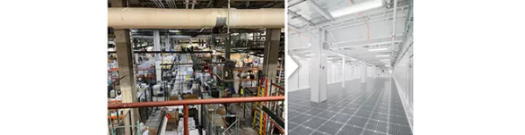
Join us for a tour of the recently renovated Beaverton factory which added a new cleanroom below the existing production cleanroom! Ryan Bestwick will lead the SEMI attendees through the chronology of this incredible fab transformation.

VISITOR PARKING INFORMATION

Analog Devices Fab Facility Tour

Registration

Early Bird (Before March 26, 2024):

Member: $75 | Non-member: $100

Regular:

Member: $100 | Non-member: $125

Registration is final. No refunds provided. No substitutions.

Lin Tso
Email: [email protected]
Phone: +1.408.943.7920

+
United States Register Now Midwest Chapter Forum Thumbnail Business Executive
The Ohio State University Logo 170x116
Advantest
ASNA 170x65
Danis Logo 170x65
Huntington Logo 170x65
IEDC 170x65
JobsOhio Logo 170x65
Lighthouse Worldwide Solutions Logo 170x65
Nordson Test Inspection Logo 170x65
One Columbus Logo 170x65

Become a Sponsor

Sponsorships can be tailored to meet your branding and marketing objectives. Become a sponsor and brand your company at the Midwest Breakfast Forum.

Contact Lin Tso, [email protected] to learn about available sponsorship opportunities.

Join us for the Midwest Chapter Forum—

What's Going on in the Silicon Heartland? Opportunities and Growth Outlook in the Semiconductor Sector

The CHIPS Act helps the U.S. regain semiconductor manufacturing leadership. The bill also advances the nation’s strengths in the semiconductor and microelectronics arena, including the automotive sector. Join us to hear executive experts, from Ohio, Michigan, and Indiana, share how their state is helping to boost the industry with significant new manufacturing projects.

SEMI Midwest Breakfast Forum is an excellent opportunity to LEARN, NETWORK, and SHARE your business solutions and ideas—Register Today!

This new regional chapter was formed to serve SEMI Members in the Midwest region. Its goal is to support member companies to grow and prosper collectively. Future chapter forums will identify, discuss, and find solutions to current topics impacting our industry. 

In-Person—Eastern Time
The Ohio State University, Ohio Union
1739 North High Street - The Great Hall Meeting Room
Columbus, OH 43210
United States

Eastern Time | Tuesday, April 9, 2024 | In-Person

8:00 am - 8:30 am

Check-In and Breakfast

8:30 am - 8:35 am
Joe Stockunas, SEMI Americas
Joe Stockunas
President
SEMI Americas

Welcome Remarks

8:35 am - 8:40 am
Dave Brewster, Managing Director, Jobs Ohio
Dave Brewster
SEMI Midwest Chapter Co-Chair and Managing Director
Jobs Ohio
Vidya Vijay
Vidya Vijay
SEMI Midwest Chapter Co-Chair and Senior Program Manager
Nordson Corporation

Welcome and Introductions

8:40 am - 8:45 am
Peter Mohler, The Ohio State University
Peter Mohler, PhD
Executive Vice President, Research Innovation & Knowledge
The Ohio State University

Keynote—Growing the Silicon Heartland Through Partnerships

8:45 am - 9:05 am
Steven Ringel, The Ohio State University
Steven A. Ringel, PhD
Distinguished University Professor, Associated Vice President for Research, Executive Director of the Institute for Materials and Manufacturing Research
The Ohio State University

Keynote—Building on Our Strengths, How Ohio State is Meeting the Challenge and Leading the Future

9:05 am - 9:30 am
Aaron Aboagye, McKinsey & Company
Aaron Aboagye
Managing Partner
McKinsey & Company

Trends and Opportunities in the Semiconductor Industry

9:30 am - 9:40 am

Break

9:40 am - 10:05 am
Duane Detwiler, Honda Research Institute
Duane Detwiler
Vice President
Honda Research Institute, Inc. USA

Sustainable Mobility Futures Research & Innovation

10:05 am - 10:30 am
Kevin Hoggatt, Intel
Kevin Hoggatt
Director of State Government Affairs for Ohio
Intel

The Silicon Heartland: Advancing American Semiconductor Manufacturing and Technology Leadership

10:30 am - 10:55 am
Chuck Bohac, Everspin Technologies
Chuck Bohac
Director of Strategic Business Development
Everspin Technologies

Evolution of the Stand Alone MRAM Technology and Markets

10:55 am - 11:30 am
Alissa Comella, The Ohio State University
Alissa Comella
Associate Vice President, Corporate Partnerships Enterprise for Research, Innovation, and Knowledge
The Ohio State University

Mobilizing the Semiconductor Workforce

Executive Panel Discussion with the Above Speakers

11:30 am
Dave Brewster, Managing Director, Jobs Ohio
Dave Brewster
SEMI Midwest Chapter Co-Chair, Managing Director
Jobs Ohio

Closing Remarks

SEMI Breakfast Forum Organized by SEMI Midwest Chapter

In-Person

Eastern Time

Hosted and Breakfast Forum Sponsored by The Ohio State University

8:00 am - 11:30 am Off Add to Calendar 2024-04-09 08:00:00 2024-04-09 11:30:00 Midwest Chapter Breakfast Forum—What's Going on in the Silicon Heartland? - Opportunity and Growth Outlook SEMI Breakfast Forum Organized by SEMI Midwest ChapterIn-PersonEastern TimeHosted and Breakfast Forum Sponsored by The Ohio State University In-Person—Eastern Time The Ohio State University, Ohio Union 1739 North High Street - The Great Hall Meeting Room Columbus, OH 43210 United States SEMI.org [email protected] America/New_York public America/New_York 2