This seminar is designed to offer a platform where executives, managers, and engineers who specialize in process development, equipment maintenance, factory automation, and manufacturing can come together to discuss ways to improve production output, increase yield and work efficiency through implementing some of AI solutions presented in this seminar.
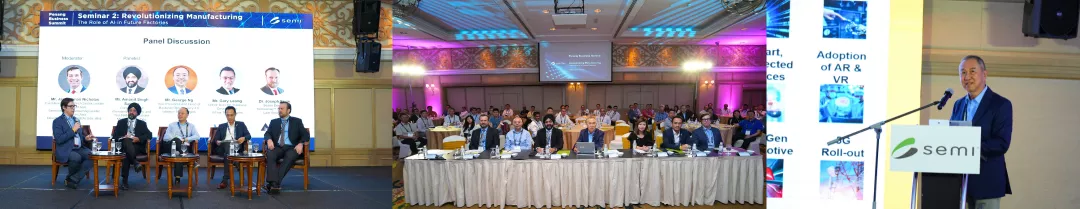
The landscape of Semiconductor manufacturing is undergoing a profound transformation, with Artificial Intelligence (AI) emerging as a driving force behind the evolution of future factories.
This theme invites participants to delve into the intricate interplay between advanced AI technologies and the manufacturing sector, showcasing the pivotal role AI plays in reshaping the entire manufacturing ecosystem.
This conference aims to provide a comprehensive platform for industry leaders, researchers, and innovators to exchange ideas, share success stories, and envision the future trajectory of manufacturing under the influence of AI.
Usual Member Rate: SGD 152 Usual Non-member Rate: SGD 227
*The above rates are inclusive of coffee/tea breaks and luncheon
30% Early Bird Rate extended until 1 March 2024!
*Malaysian Companies - HRDC Claimable for Penang Business Summit Seminar 2: Revolutionizing Manufacturing (The role of AI in Future Factories) (subject to T&C, please contact HRDC for more information). For HRDC claims, please refer to the following links on the claiming matrix and guidelines:
1:00 pm - 6:00 pm
Off
Add to Calendar2024-03-07 13:00:002024-03-07 18:00:00Penang Business Summit Seminar 2: Revolutionizing ManufacturingThe role of AI in Future FactoriesThe landscape of Semiconductor manufacturing is undergoing a profound transformation, with Artificial Intelligence (AI) emerging as a driving force behind the evolution of future factories.This theme invites participants to delve into the intricate interplay between advanced AI technologies and the manufacturing sector, showcasing the pivotal role AI plays in reshaping the entire manufacturing ecosystem.This conference aims to provide a comprehensive platform for industry leaders, researchers, and innovators to exchange ideas, share success stories, and envision the future trajectory of manufacturing under the influence of AI.*Note: Seminar 2 and Seminar 1 timing will overlap on 7 Mar Participating Fee:Usual Member Rate: SGD 152Usual Non-member Rate: SGD 227*The above rates are inclusive of coffee/tea breaks and luncheon30% Early Bird Rate extended until 1 March 2024! *Malaysian Companies - HRDC Claimable for Penang Business Summit Seminar 2: Revolutionizing Manufacturing (The role of AI in Future Factories) (subject to T&C, please contact HRDC for more information).For HRDC claims, please refer to the following links on the claiming matrix and guidelines:HRDC Approval Letter for Penang Business SummitAllowable Cost MatrixHRDC SBL Grant HelperHRDC SBL Claim Helper Contact us for enquiries!For Program: Mr. Glenn Tan | [email protected] | +65.8228.0662For Registration / HRDC Claims: Ms. Gillian Lim | [email protected] | +65.9048.1123 Presentation slides can be found HERE!Royale Chulan Penang No 1 & 2, Pengkalan Weld, Georgetown 10300 Penang Pulau Pinang MalaysiaSEMI.org[email protected]Asia/Kuala_Lumpurpublic
Asia/Kuala_Lumpur
Register Today
U.S. EPA Update on Recent PFAS Research and Regulatory Actions
The webinar will feature senior leaders and other experts from EPA and provide SEMI members with an overview of EPA’s efforts under the PFAS Strategic Roadmap; the recently finalized reporting rules under the Toxic Substances Control Act (TSCA) and the Toxics Release Inventory (TRI) program; the review and management of new PFAS chemicals under the TSCA New Chemicals program; and an update on research and development activities, including analytical test methods development. In addition to hearing directly from EPA officials on these important topics, participants will have an opportunity to ask questions at the end.
United States
Welcome Remarks
1:00 pm
Joe Stockunas
President
SEMI Americas
Speakers
Dr. Michal Freedhoff
Assistant Administrator, Office of Chemical Safety and Pollution Prevention
Join us to learn more about several of the U.S. Environmental Protection Agency’s recent actions related to PFAS and their relevance to the semiconductor manufacturing industry.
U.S. EPA Update on Recent PFAS Research and Regulatory Actions
VIRTUAL WEBINAR
1:00-2:00PM (Eastern Time)
1:00 pm - 2:00 pm
Off
Add to Calendar Disabled
America/New_York
The Summit includes strategic business and technical information for many levels and sectors of the ecosystem, including:
Government relations/advocacy staff
EHS regulatory professionals
Senior executives
Business development
Device manufacturers
Equipment suppliers
Materials suppliers
Component suppliers
Fab and facility systems construction companies
SEMI 673 South Milpitas Avenue Milpitas, CA95035 United States
8:30 am
-
9:00 am
Registration & Networking
9:00 am
-
9:05 am
James Amano
Senior Director, EHS
SEMI
Welcome
9:05 am
-
9:20 am
James Amano
Sr. Director, EHS
SEMI
Europe PFAS Restriction Proposal
9:20 am
-
9:45 am
Russ LaMotte
Principal
Beveridge & Diamond PC
US EPA PFAS Reporting rule
9:45 am
-
10:10 am
Andrew Petraszak
Tokyo Electron
Ben Kallen
SEMI
PFAS US States Proposals & Positions
10:10 am
-
10:30 am
Break
10:30 am
-
11:00 am
Lauren Crane
Lam Research
European Regulations
Including: EU Machinery Regulation, Battery Regulation, Cybersecurity Resiliency Act (CRA), AI regulation, the Ecodesign “passport” concept. UK Conformity Assessed (UKCA) mark. California fan efficiency regulation. SEMI EHS Standards update.
11:00 am
-
11:25 am
Allen Karpman
Arkema
AIM Act: HFC Allocations
11:25 am
-
11:50 am
Kristine Baranski, PE
Global Air Program Manager
Intel
AIM Act: challenges with new refrigerants
11:50 am
-
12:10 pm
Katelyn Walck
Chemours
James Snow
SCREEN
SIA PFAS Consortium
12:10 pm
-
1:15 pm
Lunch & Networking
1:15 pm
-
1:35 pm
James Amano
SEMI
SEMI PFAS Initiative
1:35 pm
-
2:00 pm
Russ LaMotte
Principal
Beveridge & Diamond
TSCA PBT: PIP, DecaBDE, What's Next?
2:00 pm
-
2:35 pm
Ben Gross
Applied Materials
Supika Mashiro
TEL
Katelyn Walck
Chemours
Lauren Crane
Lam Research
Supply Chain Inquiry Panel - sharing best practices
Plan now to join fellow semiconductor industry professionals at SEMI Headquarters in Milpitas, California for presentations and discussions around critical EHS regulatory issues impacting the industry.
Industry experts will address regulations in Europe and the United States that could significantly threaten our capability to continue manufacturing. Topics will include:
US EPA PFAS Reporting Rule
US AIM Act HFC phasedown: challenges with new refrigerants
Updates from SEMI PFAS Initiative and other collaborative industry efforts.
US EPA TSCA: PIP 3:1, DecaBDE…what's next?
Panel discussion on supply chain communication.
Plan now to attend, network and strategically prepare your company. This event is offered as an in-person briefing only.
EHS Summit 2024
Regulations, Rules, Allocations & Proposals
8:30 am - 3:30 pm
Off
Add to Calendar2024-01-25 08:30:002024-01-25 15:30:002024 EHS Summit Plan now to join fellow semiconductor industry professionals at SEMI Headquarters in Milpitas, California for presentations and discussions around critical EHS regulatory issues impacting the industry.
Industry experts will address regulations in Europe and the United States that could significantly threaten our capability to continue manufacturing. Topics will include:
US EPA PFAS Reporting Rule
US AIM Act HFC phasedown: challenges with new refrigerants
US AIM Act HFC Allocation
EU: PFAS Restriction Proposal, F-gas, Revised Machinery Regulation, Revised Battery Regulation, Pending Cybersecurity resiliency regulation, Pending AI regulation, the ecodesign “passport” concept.
Updates from SEMI PFAS Initiative and other collaborative industry efforts.
US EPA TSCA: PIP 3:1, DecaBDE…what's next?
Panel discussion on supply chain communication.
Plan now to attend, network and strategically prepare your company. This event is offered as an in-person briefing only.SEMI 673 South Milpitas Avenue Milpitas, CA 95035 United StatesSEMI.org[email protected]America/Los_Angelespublic
America/Los_Angeles
Many semiconductor-based systems are moving toward 2.5D and 3D designs consisting of different pre-manufactured chips (chiplets) that perform specific functions. These are often provided by multiple vendors and are typically interconnected using an interposer. However, unlike monolithic multi-function chips, chiplets can be developed anywhere and at any process node. As such, chiplets from untrusted vendors can be unreliable or malicious. Third parties can reverse engineer, overproduce, or steal the IP of chiplets. Consequently, they raise new security challenges for an industry still figuring out ways to effectively mitigate hardware security threats to monolithic chips.
The webinar will focus on the potential threats that occur at the different stages of bringing chiplets to life, including design, assembly, and testing. The panelists will assess current safeguards to mitigate these risks and discuss open challenges for industry and academia.
ESDA Webinar: Chiplet Security—Current and Future
VIRTUAL WEBINAR
9:00-10:00AM (Pacific Time)
9:00 am - 10:00 am
Off
Add to Calendar Disabled
America/Los_Angeles
Register Now
Electromagnetic Interference and Electrical Overstress Management: Why, What, and How
Electromagnetic interference (EMI) is becoming more critical in all aspects of semiconductor manufacturing, affecting productivity and yield.
The SEMI E176 Standard, "Guide to Assess and Minimize Electromagnetic Interference (EMI) in a Semiconductor Manufacturing Environment," addresses this issue. This document provides practical, actionable guidance on establishing an acceptable EMI environment in semiconductor processes: from assessing the EMI environment to EMI mitigation to verification. SEMI E176 sets recommended EMI limits for different process categories. The Standard can benefit every stage of the semiconductor process and electronic assembly.
1. Overview of SEMI and SEMI Standards
- SEMI as a resource for your company
2. EMI and EMC - an overview
3. Effect of EMI on processes and equipment
- EMI and Electrical Overstress
- Equipment precision
- Process variations
- Other problems
4. Sources and propagation of EMI
5. Overview of SEMI E.33
- Emphasis on Table 1: Compliance Assignment/Responsibility Table
6. Overview of SEMI E.176
7. Basics of a viable EMI program at a factory based on SEMI E.176
- Purpose
- Structure
- Resources and budget
- Similarity and synergy with already-existing ESD program
Join us for a hybrid experience with both in-person and virtual attendance options.
Electromagnetic Interference and Electrical Overstress Management
Why, What, and How
An executive overview course
December 18, 2023
4:00 pm - 5:00 pm
Off
Add to Calendar2023-12-18 16:00:002023-12-18 17:00:00EMI and EOS Management CourseJoin us for a hybrid experience with both in-person and virtual attendance options.SEMI HQ CA United StatesSEMI.org[email protected]America/Los_Angelespublic
America/Los_Angeles
Register now
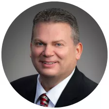
Leveraging the CHIPS Act in the Silicon Heartland: Ohio Semiconductor Industry Initiatives
SEMI has invited key stakeholders from Ohio to discuss state initiatives that can be leveraged in alignment with current and upcoming CHIPS Funding opportunities. Webinar participants will learn why Ohio is a premier location for semiconductor operations and what government initiatives are available to strategically complement competitive CHIPS proposals. JobsOhio, the state’s unique private economic development corporation, acts as a catalyst for high-growth business investments and job creation that are helping propel the state’s ingenuity and ambitions forward.
Meet the Speakers
Joe Stockunas
President
SEMI Americas
David Brewster
Managing Director, Technology Sector
JobsOhio
Join us for a 2-day working session to align our industry on concrete next steps to secure semiconductor manufacturing against an ever-evolving threat environment. With our complex and interconnected supply chains, no single company can be safe unless all companies are safe. Our consortium of device makers, foundries, equipment makers, component suppliers, and software suppliers are working together to rapidly develop a practical plan to improve security now, and for years to come while minimizing costs and avoiding duplication.
• Consortia governance, structure, deliverables, and roadmap for 2024
• E187 SEMI Standard implementation ideation session
• Develop a method to survey, evaluate, and certify manufacturing equipment cybersecurity protections
• Globalization of SEMI Taiwan’s E187 reference architecture and checklist
Day 2: December 7, 2023 - 8 am - 3 pm PT
8:00 am
-
3:00 pm
• Opportunities for collaboration and information sharing for cyber threats and incidents
• Supply Chain Cybersecurity working session
• Create a semiconductor industry-specific framework to measure security and implementation approach across the entire ecosystem
• Review NIST industry profiles and evaluate for suitability in semiconductor
• Next steps: Including forming working groups and assigning leaders
Join us for a 2-day workshop aimed at developing and advocating a practical, standards-based, industry-wide approach to improving cybersecurity and resilience across the semiconductor supply chain.
Time:
Day 1: Noon - 7 pm PT
Day 2: 8 am – 3 pm PT
In-person registration has reached capacity. However, you can still register to participate online.
SEMI Cybersecurity Launch Workshop
December 6-7, 2023
Off
Add to Calendar Disabled
America/Los_Angeles
Register now
Navigating Semiconductor industry in Malaysia: Challenges & Opportunities for young engineers
This coffee talk session serves as an informal and insightful dialogue for young engineers entering the dynamic semiconductor industry in Malaysia. The discussion focuses on the challenges and opportunities that await them in this vibrant sector. Malaysia's semiconductor landscape is thriving, with numerous multinational corporations contributing significantly to the global supply chain. However, as with any dynamic industry, challenges exist, including staying current with technological advancements, navigating global competition, ensuring quality and reliability, adhering to environmental and regulatory standards, and preparing for potential supply chain disruptions.
Amidst these challenges lies a world of opportunities for young engineers. The semiconductor industry offers an ideal platform for innovation, career growth, global exposure, societal impact, and networking. This session offers valuable recommendations, including embracing lifelong learning, seeking mentorship, building a professional network, cultivating adaptability, finding purpose in work, and maintaining a healthy work-life balance.
The session will emphasize the need to embrace challenges as stepping stones to success while seizing the opportunities to make a meaningful impact in the semiconductor industry. It is an encouragement to the young engineers, assuring them that their talent and determination will leave a significant mark on the industry's landscape.
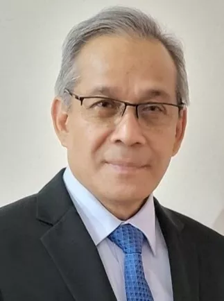
About Speaker:
Encik Noorazidi Bin Che Azib
Deputy Vice President, Operation Technology, Strategic Program (OTSP), Inari-Amerton Bhd
Noorazidi (Azidi), a Mechanical Engineering graduate from the University of Nevada, Reno, USA, currently holds the position of Deputy Vice President at INARI, overseeing OTSP (Operation Technology and Strategic Programs) and EHS (Environment, Health, and Safety). Azidi began his career in high-volume semiconductor manufacturing, process engineering, automation system design, Industry 4.0, and environmental sectors, accumulating 35 years of experience at multinational corporations such as AMD, Hewlett Packard, Agilent, and Avago before joining INARI in 2012.
He played a pivotal role in INARI's transformation towards digitalization and the adoption of cyber-physical systems. Known for his passion for innovation and commitment to talent development, he collaborates closely with local academia and industrial skill development centers, helping to prepare over 3,000 interns in the past five years for industry roles.
Azidi's expertise in Industry 4.0 has made him a key figure in collaborations with government agencies, actively supports the development of electrical and electronic supply chains, local small-medium-enterprises (SME) productivity, adoption of advanced technology, and business development. Together with the Group CEO, Mr KC Lau, INARI has also initiated numerous SME development programs under the Inari Waterfall Effect Model, which in line with their Industry 4.0 Roadmap.
Attendee Fees: RM 120 / pax
- Goodie bag, snacks, and drinks are included for session
2:00 pm - 5:00 pm
Off
Add to Calendar2023-11-30 14:00:002023-11-30 17:00:00Tech Talk Over Coffee | Malaysia, PenangNavigating Semiconductor industry in Malaysia: Challenges & Opportunities for young engineersThis coffee talk session serves as an informal and insightful dialogue for young engineers entering the dynamic semiconductor industry in Malaysia. The discussion focuses on the challenges and opportunities that await them in this vibrant sector. Malaysia's semiconductor landscape is thriving, with numerous multinational corporations contributing significantly to the global supply chain. However, as with any dynamic industry, challenges exist, including staying current with technological advancements, navigating global competition, ensuring quality and reliability, adhering to environmental and regulatory standards, and preparing for potential supply chain disruptions.Amidst these challenges lies a world of opportunities for young engineers. The semiconductor industry offers an ideal platform for innovation, career growth, global exposure, societal impact, and networking. This session offers valuable recommendations, including embracing lifelong learning, seeking mentorship, building a professional network, cultivating adaptability, finding purpose in work, and maintaining a healthy work-life balance.The session will emphasize the need to embrace challenges as stepping stones to success while seizing the opportunities to make a meaningful impact in the semiconductor industry. It is an encouragement to the young engineers, assuring them that their talent and determination will leave a significant mark on the industry's landscape. About Speaker: Encik Noorazidi Bin Che AzibDeputy Vice President, Operation Technology, Strategic Program (OTSP), Inari-Amerton BhdNoorazidi (Azidi), a Mechanical Engineering graduate from the University of Nevada, Reno, USA, currently holds the position of Deputy Vice President at INARI, overseeing OTSP (Operation Technology and Strategic Programs) and EHS (Environment, Health, and Safety). Azidi began his career in high-volume semiconductor manufacturing, process engineering, automation system design, Industry 4.0, and environmental sectors, accumulating 35 years of experience at multinational corporations such as AMD, Hewlett Packard, Agilent, and Avago before joining INARI in 2012.He played a pivotal role in INARI's transformation towards digitalization and the adoption of cyber-physical systems. Known for his passion for innovation and commitment to talent development, he collaborates closely with local academia and industrial skill development centers, helping to prepare over 3,000 interns in the past five years for industry roles.Azidi's expertise in Industry 4.0 has made him a key figure in collaborations with government agencies, actively supports the development of electrical and electronic supply chains, local small-medium-enterprises (SME) productivity, adoption of advanced technology, and business development. Together with the Group CEO, Mr KC Lau, INARI has also initiated numerous SME development programs under the Inari Waterfall Effect Model, which in line with their Industry 4.0 Roadmap. Attendee Fees: RM 120 / pax- Goodie bag, snacks, and drinks are included for sessionContact: [email protected] for any questions Register Now!Macallum Connoisseurs 1, Gat Lebuh Macallum, 10300 George Town, Pulau Pinang, Malaysia Penang MalaysiaSEMI.org[email protected]Asia/Kuala_Lumpurpublic
Asia/Kuala_Lumpur
SIGN UP
Mesoline’s 3D Micro Printing Technology & Microchannel Particle Deposition
Introduction to Mesoline’s Emerging 3D Micro Printing Technology, Microchannel Particle Deposition (MPD), Used for MEMS & Sensors
Mesoline’s Microchannel particle deposition (MPD) is a wafer-scale thick-film deposition process where a polymeric stamp is used to transfer ink onto a substrate. This novel microfabrication technology offers ultra-small and reproducible micro features fabricated with extensive parallelization and high scalability. Unique process features include: (1) full wafers patterning in 15-minutes, (2) 1 to 50mm structures with up to 5/1 aspect ratios and 3) full 3D-control of the printed structures. Many different sensor applications of this technology will be introduced, including: (1) printing sensing electrodes for metal oxide gas sensors, (2)printing of getters for microbolometers, (3) printing of porous electrodes for biosensing applications and (4) accurate deposition of glass frit for advanced packaging applications.
8:00 am - 9:00 am
Off
Add to Calendar2023-12-06 08:00:002023-12-06 09:00:00Mesoline’s 3D Micro Printing Technology & Microchannel Particle DepositionIntroduction to Mesoline’s Emerging 3D Micro Printing Technology, Microchannel Particle Deposition (MPD), Used for MEMS & Sensors
Mesoline’s Microchannel particle deposition (MPD) is a wafer-scale thick-film deposition process where a polymeric stamp is used to transfer ink onto a substrate. This novel microfabrication technology offers ultra-small and reproducible micro features fabricated with extensive parallelization and high scalability. Unique process features include: (1) full wafers patterning in 15-minutes, (2) 1 to 50mm structures with up to 5/1 aspect ratios and 3) full 3D-control of the printed structures. Many different sensor applications of this technology will be introduced, including: (1) printing sensing electrodes for metal oxide gas sensors, (2)printing of getters for microbolometers, (3) printing of porous electrodes for biosensing applications and (4) accurate deposition of glass frit for advanced packaging applications.United StatesSEMI.org[email protected]America/Los_Angelespublic
America/Los_Angeles
Register Now
Sponsorships can be tailored to meet your branding and marketing objectives. Become a sponsor and brand your company at the Arizona & Texas Virtual Forum.
Contact Lin Tso, [email protected] to learn about available sponsorship opportunities.
ONSHORING AND SUPPLY CHAIN OPPORTUNITIES
In this dynamic online gathering, industry leaders, experts, and stakeholders come together to explore the burgeoning landscape of onshoring and supply chain development in the United States. This forum serves as a pivotal hub for insightful discussions about the immense potential of the United States to reshape the manufacturing and distribution sectors.
Discover a wealth of knowledge from Alvarez & Marsal, DSV, EMD Electronics, Gartner, Huntsman, and Intel on:
Economic, infrastructural + regulatory factors
Rebalancing + expanding the supply chain
Investments that make the United States a prime destination for onshoring
And much more
Gain a comprehensive understanding of the advantageous attributes that draw businesses to establish and expand their operations in the US, including strategic geographic locations, advanced transportation networks, and access to skilled talent pools.
Other topics will include the intricacies of supply chain optimization, risk mitigation, resilience-building strategies, and driving economic growth and sustainability through localized production and distribution networks. The reshaping of global supply chains, reducing dependency on foreign production, and enhancing end-to-end logistical efficiency will also be discussed.
Discover a wealth of knowledge as speakers unveil insights into the economic, infrastructural, and regulatory factors for prime destinations for onshoring.
Fall Outlook: Onshoring and Supply Chain Opportunities
[WEBINAR]
Presented by the SEMI Arizona & Texas Chapters
November 15, 2023
PACIFIC | 9:00–10:30am ♦ MOUNTAIN | 10:00–11:30am
CENTRAL | 11:00am–12:30pm ♦ EASTERN | 12:00 –1:30pm
9:00 am - 10:30 am
Off
Add to Calendar Disabled
America/Los_Angeles
2