Off
Add to Calendar2026-02-11 00:00:002026-02-13 00:00:00SEMICON Korea 2026TRANSFORM TOMORROWThe future of the semiconductor industry starts here.Join us at SEMICON Korea 2026 to shape tomorrow together. HoursFebruary 11, 2026 | 10:00-17:00 (Last entry 16:30)February 12, 2026 | 10:00-17:00 (Last entry 16:30)February 13, 2026 | 10:00-16:00 (Last entry 15:30)VenueCOEX (Hall A, B, C, D, E, Grand Ballroom, Platz and ASEM Ballroom)Westin Seoul ParnasGrand InterContinental Seoul ParnasScale550 Exhibitors, 2409 booths (2025: 501 exhibitors, 2301 booths)Seoul South KoreaSEMI.org[email protected]America/Los_Angelespublic
Early-bird Registration Close: 3 pm, Friday, May 12(KST)
Registration Fee
Early Bird (~ May 12)
SEMI Member: KRW 280,000
Non Member: KRW 330,000
On site
SEMI Member/ Student : KRW 330,000
Non Member: KRW 380,000
※ Group registration fee applies if more than 5 people are registered from one company. Please contact us by email ([email protected] ) for group registration.
Convention Hall 2, Suwon Convention Center Suwon-si Gyeonggi-do South Korea
9:00 am
-
9:05 am
Welcome
Keynote
9:05 am
-
9:35 am
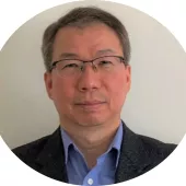
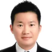
Namsung Kim
Senior Director
Applied Materials
GAA(Gate-All-Around) technology to enable continuous CMOS transistor scaling for energy efficient computing solution
Namsung Kim is a Senior Director in the Integrated Module Solutions (IMS) Group at Applied Materials. He is currently responsible for managing customer engagement programs, driving business growth, and leading cross-functional teams (various Business Units) to deliver the integrated materials/modules-base product solutions across leading-edge CMOS Logic and Memory technologies. Prior to this role, he has successfully led & accomplished the definition of CMOS Logic technology roadmap, its inflections of future technology nodes and delivered multiple product development paths by validating innovative pathway solutions.
He joined Applied Materials, Inc., USA in 2015, bringing over 20 years of semiconductor device/process integration experiences (various engineering/management positions) from both CMOS Logic (GlobalFoundries/IBM alliance in USA and SSMC in Singapore) and Memory (SK-Hynix, previously LG Semi., in Korea) industries. He earned a MS in electrical and computer engineering from the National University of Singapore. He has authored and co-authored more than 50 technical publications and holds over 40 patents in the field of advanced logic (FinFETs and GAA devices) and memory technologies.
Market & Technology Trends for Memory Devices including Materials
Dr. Jeongdong Choe is a Senior Technical Fellow at TechInsights. He has over 30 years of experience in the semiconductor industry, R&D, and reverse engineering on DRAM, NAND/NOR FLASH, SRAM/Logic, and Emerging Memory. He worked for SK Hynix and Samsung Electronics for over 20 years. He joined TechInsights and has been focusing on technology analysis of semiconductor processes, materials, devices, and architecture. He has written many articles on memory technology including roadmaps, technology trends, and detailed comparisons.
Session 1: Advanced Materials for Enabling Next-Generation Devices
10:50 am
-
11:15 am
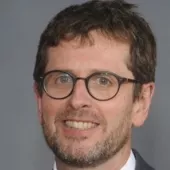
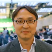
Jean-Marc Girard
CTO and Sr. VP
Air Liquide
Precursors for Memory
Jean-Marc Girard Ph.D. is CTO and Sr. VP of Manufacturing Technologies at Air Liquide Advanced Materials (ALAM), and an Air Liquid Group Fellow. He has 25 years of experience of R&D and product development management in the field of semiconductor materials and process technology in Europe, Japan and the US, and is one of the founders and was the global director of ALOHA™ from 2005 to 2010 (Air Liquide’s original CVD/ALD materials product line).
Within ALAM, Jean-Marc globally manages the Research and Development for deposition & advanced dry etching materials, oversees strategic engagements and collaborations with leading customers and equipment companies, and supervises the Intellectual Property generation and portfolio management. Since 2021, Jean-Marc’s role has expanded to leading packaging and manufacturing technology developments efforts.
11:15 am
-
11:40 am
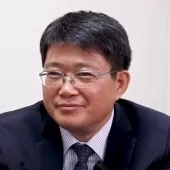
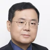
Andy Kim
Sr. Director
Lam Research
Materials Trends in Semiconductor Manufacturing
“Byunghee Kim” has been Sr. Technologist in Lam Research since 2017.
Prior to joining Lam Research, “Kim” was director position for Samsung Electronics. During his 23 years at Samsung Electronics, “Kim” spent time doing module development, including gate, contact and BEOL.
“Kim” received a bachelor’s degree in chemistry from Yonsei Univ., Seoul, Korea and a master’s degree in MSE from Seoul Nat’l Univ., Seoul, Korea.
Jeongsik Kim, received a MS degree in Organic Synthetic Chemistry from Sogang University(Korean) in 2006 and then joined Dongjin Semichem. He had developed the patterning process materials such as bottom antireflective coating(BARC), spin on hardmask(SOH), photoresist materials in Semiconductor Materials Business Division since 2006. In 2013, he had joined the advanced lithography program of IMEC(Belgium) as Dongjin Semichem assignee and researched the ArF immersion patterning and defectivity for two years. Currently, he is in charge of developing EUV photoresist at Dongjin Semichem.
Sung Ho Kim is the Head of Specialty Gases Marketing, Clean & Etch platform, Merck KGaA, Darmstadt, Germany where he drives the execution of product marketing strategy to meet with industry’s dry etch and chamber clean gas technical and commercial needs, and leads product life cycle management and NPI (New product introduction) initiatives to help customers to advance its dry etch and chamber clean process performance. He is a proven business leader with more than 20 years of experience in the semiconductor materials industry, with a wide range of leadership experience in product marketing, product management, and technical/engineering expertise. He is based in Pangyo, Korea. Sung-Ho received a bachelor's degree in Chemical Engineering from Seoul National University.
Head of BASF Electronic Materials R&D Center in Suwon
BASF
Aiming CO2 neutrality – Sustainable Solutions for IC Applications
Won-Seob Cho, Ph.D. presently serves as the Head of the BASF Electronics Materials R&D Center in Suwon, Korea. In this esteemed position, he is responsible for leading research teams dedicated to the development of advanced wet chemical solutions, such as advanced cleaning and electroplating methods. He boasts over 20 years of research and development experience, particularly in the formulation and electrochemical screening of solutions.
Prior to joining BASF a decade ago, He served as a Principal Researcher at Samsung SDI and Samsung Fine Chemicals, where he specialized in developing planarization and electroplating solutions. Notably, his research interests have recently expanded to encompass the Advanced Package field.
Won-Seob Cho holds a distinguished Ph.D. in Chemistry from the University of Texas at Austin and has also served as a postdoctoral fellow in Supramolecular Chemistry at the University of California at Los Angeles, further solidifying his scientific expertise.
Carbon Neutral Strategy of Korean Government and Role of Material Companies
Dr. Nam, Sang Uk is conducting various studies on the ICT (semiconductor, display) industry based on economics at the KIET (Korea Institute of Industrial Research), a national research institute.
Since joining the KIET in 2018, he has participated in various studies on ICT industry policies such as Japanese export regulations, development strategy of material, parts and equipment, global value chain, and digital transformation.
In the field of carbon neutrality, he participated in major reports such as the semiconductor and display industry's carbon neutral promotion strategy and policy tasks, and the impact of RE100 on Korea's major export industries.
Materials still matter. Trends in materials demand and supply.
Mark Thirsk is Managing Partner of Linx Consulting, a leading management and strategic consulting company for electronic materials.
Mark Thirsk has experience spanning many materials and processes in wafer fabrication, combined with economic and business forecasting, strategic planning, technical marketing and M&A experience. Mark has worked in materials and equipment development, marketing, applications support, and production, as well as having expertise in business incubation, strategic development, and M&A. Mark is well placed to bring clarity and insight to market analysis from both a technical and commercial perspective. Additionally, Mark has been active in SEMI since 1999, volunteering in industry advocacy, education, and recruiting.
Mark has worked in the UK, Germany, Belgium, and the USA. Mark holds an Honours B.Sc. in Metallurgy and Materials Science from Birmingham University and an MBA
E. Jan Vardaman is president and founder of TechSearch International, Inc., which has provided market research and technology trend analysis in semiconductor packaging since 1987. She is the author of numerous publications on emerging trends in semiconductor packaging and assembly. She is a senior member of IEEE EPS and is an IEEE EPS Distinguished Lecturer. She received the IMAPS GBC Partnership award in 2012, the Daniel C. Hughes, Jr. Memorial Award in 2018, the Sidney J. Stein International Award in 2019, and she is an IMAPS Fellow. She is a member of MEPTEC, SMTA, and SEMI. Before founding TechSearch International, she served on the corporate staff of Microelectronics and Computer Technology Corporation (MCC), the electronics industry’s first pre-competitive research consortium.
Re-visioning Material Technology for Sustainable Resource Utilization and Supply Chain
Sam-Jong Choi, Ph.D. has been working as a material expert at Samsung Electronics Semiconductor for over 30 years. He joined the company in 1991 and has been responsible as a material engineer and expert for Memory Manufacturing Technology Center in Samsung Electronics by now. He obtained a Ph.D in Electronic, Computer, and Telecommunication Engineering from Hanyang University in 2020.
In 2019, he was promoted to Group Leader for Memory Material Technology Group, where he oversaw the development of new materials and quality management for Samsung Electronics. In 2020, Samjong Choi was appointed as an Corporate VP at Samsung Electronics, where he continues to play a key role in the field of semiconductor material.
As an experienced engineer and leader, he brings a wealth of knowledge and expertise to his current role, making Samsung Electronics stay at the forefront of technological innovation in the global semiconductor material industry.
In the semiconductor industry, a stable and efficient global supply chain is as important as the continuous development of advanced technology. In addition to the trade conflict and reshoring, new trends such as GWP(Global Warming Potential) are highlighted, and prompt response of the Ecosystem is essential. Accordingly, SMC Korea is trying to provide an opportunity for the semiconductor industry to discuss issues that need to be spoken out together.
SMC Korea 2023 prepares various presentations to share information on the latest technologies and markets through the participation of global leading companies while also checking global warming potential (GWP) in terms of materials. Please join us in the insights of global experts!
SMC (Strategic Materials Conference) Korea 2023
May 17(Wed), 2023 | Convention Hall 2, Suwon Convention Center
Off
Add to Calendar2023-05-17 00:00:002023-05-17 00:00:00SMC Korea 2023Semiconductor Materials for Sustainable Future
In the semiconductor industry, a stable and efficient global supply chain is as important as the continuous development of advanced technology. In addition to the trade conflict and reshoring, new trends such as GWP(Global Warming Potential) are highlighted, and prompt response of the Ecosystem is essential. Accordingly, SMC Korea is trying to provide an opportunity for the semiconductor industry to discuss issues that need to be spoken out together.
SMC Korea 2023 prepares various presentations to share information on the latest technologies and markets through the participation of global leading companies while also checking global warming potential (GWP) in terms of materials. Please join us in the insights of global experts!Convention Hall 2, Suwon Convention Center Suwon-si Gyeonggi-do South KoreaSEMI.org[email protected]Asia/Seoulpublic
Asia/Seoul
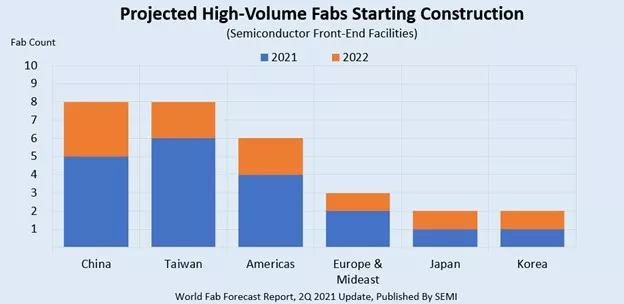
글로벌 전자산업 공급망을 대표하는 산업 협회인 SEMI의 ‘팹 전망 보고서(World Fab Forecast)’에 따르면 급격하게 증가하는 통신, 컴퓨팅, 헬스케어, 온라인 서비스, 차량용 반도체 등의 수요를 충족하기위해 올해 말까지 19개의 신규 팹이 착공되며, 2022년에는 10개의 팹이 추가로 더 착공될 것으로 보인다.
SEMI의 CEO인 아짓 마노차(Ajit Manocha)는 "세계적인 칩 부족 문제를 해결하기위해 신설될 29개 팹의 장비 투자액은 향후 몇 년간 1,400억 달러를 넘어설 것으로 예상된다.”고 말했다. 이어 그는 "중장기적으로 전 세계 팹의 생산력 확대는 자율주행차, 인공지능, 고성능 컴퓨팅, 5G~6G 통신 등 새로운 애플리케이션에 따른 반도체 수요 증가에 부응할 것"이라고 덧붙였다.
2022년까지 중국과 대만에 각각 8개, 북미 6개, 유럽 및 중동 3개, 일본과 한국에 각각 2개의 팹이(총 29개) 착공될 예정이다. 300mm 웨이퍼를 생산하는 팹은 2021년 15곳, 2022년에는 7곳이 착공에 들어간다. 나머지 7개의 팹은 100mm, 150mm, 200mm 웨이퍼를 생산하는 팹이다. 2022년까지 착공에 들어가는 팹의 전체 생산량은 월간 260만장 웨이퍼(200mm 웨이퍼 면적 기준)에 달할 것으로 전망된다.
2021년부터 2022년까지 착공되는 29개의 팹 중 15개는 파운드리 팹이며 200mm웨이퍼 기준 월간 생산량은 웨이퍼 3만에서 22만장 수준이다. 메모리 팹은 4개가 건설될 예정이며 200mm 웨이퍼 기준 월간 생산량은 10만에서 40만장 수준이다.
착공 후에 반도체 장비 설치까지는 보통 2년이 소요되기 때문에 올해 착공을 시작하는 팹 중 대다수는 2023년까지 반도체 장비 도입이 시작하지 않을 것으로 보인다. 하지만 일부 팹에는 이르면 내년 상반기부터 반도체 장비가 설치될 것으로 전망된다.
SEMI의 팹 전망 보고서에 따르면 내년에는 10개의 팹이 착공될 예정이지만 이 숫자는 칩 메이커의 결정 여부에 따라 더 증가할 수도 있다. 건설 예정인 팹의 생산량, 제품, 기술 등에 대한 자세한 내용은 SEMI 팹 전망 보고서를 통해 확인할 수 있다.
※ Group registration fee applies to groups of five or more from the same company. ※ For group registration inquiries, please contact SEMI Korea Program Team at [email protected].
Convention Hall 1, 3F, Suwon Convention Center South Korea South Korea
8:30 am
-
9:00 am
Welcome Reception
9:00 am
-
9:30 am
Gun-chang Roh
Hyundai Motor Securities
Overview
9:30 am
-
10:00 am
Chee ping Lee
Lam Research
Making 3DIC Manufacturable for AI: From Vertical Integration to Scalable Production
As AI systems push requirements for higher bandwidth, lower power, and increased integration density, 3D integrated circuits (3DIC) are moving rapidly from development to production. However, scaling 3DIC introduces complex application challenges across the manufacturing flow, where process interactions and control become critical.
This talk examines key 3DIC applications and process challenges, including high aspect ratio TSV etch, void free TSV fill, and dielectric deposition, required for reliable wafer and die level stacking. Emerging applications such as inter die gap fill for advanced chiplets integration and plasma dicing for improved yield, edge quality, and die strength further increase integration complexity and productivity demands.
The presentation highlights Lam Research innovations across etch, deposition and clean processes that enable tighter process windows, improved uniformity, and higher throughput. In addition, equipment intelligence and data driven control are increasingly essential to enhance yield learning and manufacturing productivity. Together, these advances are enabling scalable, high volume 3DIC manufacturing for next generation AI systems.
The rapid electrification of automotive and industrial systems is placing increasingly stringent demands on power semiconductor devices in terms of voltage capability, thermal performance, reliability, and system integration. This presentation reviews recent trends in power devices and power module packaging technologies aimed at improving performance while addressing cost and manufacturability constraints.
First, the fundamental differences between digital and power devices are outlined, followed by an overview of power device applications based on silicon (Si), silicon carbide (SiC), and gallium nitride (GaN) technologies, together with Amkor’s product portfolio.
Next, power module packaging technologies are discussed with a focus on key electrical and thermal challenges. Representative solutions, including advanced interconnects, cooling architectures, and embedded power modules, are introduced, along with a brief overview of Amkor’s technology roadmap.
Finally, the role of the Amkor Technology Japan R&D Center in supporting open innovation and global collaboration is briefly discussed.
Co-packaged optics (CPO) is emerging as a key enabler for scaling bandwidth while containing power and cost in next-generation AI and cloud infrastructure. By moving optical engines closer to the switch ASIC and shortening high-speed electrical reaches, CPO can reduce SerDes power, ease signal-integrity constraints, and increase overall front-panel bandwidth density. However, delivering these benefits at volume requires new approaches across package architecture, manufacturing, and system integration.
This presentation reviews the main packaging challenges that must be solved to industrialize CPO, including thermal management and heat spreading near high-power silicon, fiber attach and optical alignment tolerances, photonics/laser integration choices, high-density optical and electrical I/O, substrate and interposer selection, and reliability risks such as warpage, CTE mismatch, and contamination control. Test and rework strategy, yield learning, and supply-chain readiness (materials, assembly, and metrology) are highlighted as practical barriers to adoption.
The talk also outlines opportunities created by CPO packaging innovations—such as modular optical tiles, standardized fiber interfaces, advanced lid/heat-sink concepts, and co-design of electrical, mechanical, and optical domains—to unlock higher radix switches and lower system power. Attendees will leave with a structured view of technology tradeoffs, a roadmap of near-term versus long-term packaging options, and actionable considerations for bringing CPO from prototypes to deployable products.
Advanced Packaging Summit 2026, under the theme “Packaging the Future of AI – From Silicon to Photon,” will examine the evolution of packaging technologies in the AI era and their broader implications for the semiconductor industry. Featuring presentations by leading industry experts, the summit will explore market shifts driven by the growing demand for AI semiconductors, along with key technologies enabling advanced packaging. The program will also highlight the innovation journey from silicon-based integration technologies to photonics-based interconnects, which are essential to enhancing packaging productivity and scalability. Panel discussions in each session will further provide opportunities to exchange insights on real-world applications, technical challenges, and possibilities for cross-industry collaboration, while exploring new business opportunities and strategic perspectives created by advanced packaging technologies in the AI era.
ADVANCED PACKAGING SUMMIT 2026
July 15(Wed), 2026 | Convention Hall 1, 3F, Suwon Convention Center
8:30 am - 5:00 pm
Off
Add to Calendar2026-07-15 08:30:002026-07-15 17:00:00ADVANCED PACKAGING SUMMIT 2026Advanced Packaging Summit 2026, under the theme “Packaging the Future of AI – From Silicon to Photon,” will examine the evolution of packaging technologies in the AI era and their broader implications for the semiconductor industry. Featuring presentations by leading industry experts, the summit will explore market shifts driven by the growing demand for AI semiconductors, along with key technologies enabling advanced packaging. The program will also highlight the innovation journey from silicon-based integration technologies to photonics-based interconnects, which are essential to enhancing packaging productivity and scalability. Panel discussions in each session will further provide opportunities to exchange insights on real-world applications, technical challenges, and possibilities for cross-industry collaboration, while exploring new business opportunities and strategic perspectives created by advanced packaging technologies in the AI era.Convention Hall 1, 3F, Suwon Convention Center South Korea South KoreaSEMI.org[email protected]Asia/Seoulpublic
Asia/Seoul
Setting the Stage: Industry Drivers & SCC Initiative Context
• Semiconductor Industry Decarbonization Challenges
• The Need for Quantified Business Cases
• SCC Initiative Background & Development Journey
• Vision for Industry Adoption & Collaboration
• Tool Architecture & Methodology
• Key Inputs & Assumptions
• Understanding the Outputs & Metrics
• Live Demonstration & Example Scenario
• Current Limitations & Future Development Opportunities
9:36 am
-
9:50 am
Jeff Rudnik
Director of Environmental Sustainability & Net Zero
ASM
Industry Use Cases & Practical Applications
• Evaluating Decarbonization Projects
• Comparing Alternative Mitigation Strategies
• Supporting Internal Investment Decisions
• Lessons Learned from Early Applications
• Opportunities for Industry Collaboration
The semiconductor industry is under increasing pressure to decarbonize its operations, particularly with regard to Scope 1 emissions — direct greenhouse gas emissions (GHG) from owned or controlled sources. Yet many companies face a persistent challenge: how to make a clear, consistent, and financially credible case for emissions reduction investments. To help address this need, the Semiconductor Climate Consortium (SCC) has developed a Cost-Benefit Calculator — a simplified and flexible tool that offers a structured starting point for evaluating carbon emissions reduction projects. The calculator enables users to estimate the Net Present Cost (NPC) per ton of CO₂ equivalent emissions reduction, helping to translate environmental impact into business-relevant terms.
Join the SEMI's Semiconductor Climate Consortium (SCC) Scope 1 Working Group and document authors for a webinar discussing their journey creating the Cost-Benefit Calculator and outlining the use cases for this tool. The Cost-Benefit Calculator is a functional spreadsheet with built in report creation tools. For business managers who need to calculate emissions for Scrope 1.
Building the business case for emission reductions
9:00 am - 10:00 am
Off
Add to Calendar2026-06-16 09:00:002026-06-16 10:00:00SCC: Cost Benefit Calculator WebinarThe semiconductor industry is under increasing pressure to decarbonize its operations, particularly with regard to Scope 1 emissions — direct greenhouse gas emissions (GHG) from owned or controlled sources. Yet many companies face a persistent challenge: how to make a clear, consistent, and financially credible case for emissions reduction investments. To help address this need, the Semiconductor Climate Consortium (SCC) has developed a Cost-Benefit Calculator — a simplified and flexible tool that offers a structured starting point for evaluating carbon emissions reduction projects. The calculator enables users to estimate the Net Present Cost (NPC) per ton of CO₂ equivalent emissions reduction, helping to translate environmental impact into business-relevant terms.Join the SEMI's Semiconductor Climate Consortium (SCC) Scope 1 Working Group and document authors for a webinar discussing their journey creating the Cost-Benefit Calculator and outlining the use cases for this tool. The Cost-Benefit Calculator is a functional spreadsheet with built in report creation tools. For business managers who need to calculate emissions for Scrope 1.SCC members can download the Cost Benefit Calculator Report here.SEMI United StatesSEMI.org[email protected]America/Los_Angelespublic
America/Los_Angeles
Register Today!
Beneq Appoints Dr. Jason Harrison as Chief Executive Officer
Semiconductor industry leader takes the helm to accelerate Beneq’s next phase of growth in atomic layer deposition
Espoo, Finland, 8 May, 2026 – Beneq Oy, the home of atomic layer deposition (ALD), today announced the appointment of Dr. Jason Harrison as Chief Executive Officer. Dr. Harrison succeeds Dr. Tommi Vainio and will lead Beneq into its next phase of growth across semiconductor, optical, and emerging technology markets.
A Strategic Leadership Transition
Beneq enters its next phase of growth from a position of strong commercial momentum. Recent milestones include the qualification of the Beneq Transform® cluster tool for volume production of GaN power and RF filter devices; the introduction of Beneq Transmute™ and Beneq Transform® XP, both engineered for high-volume manufacturing (HVM) of specialty semiconductors; growing adoption of the P-Series for coating critical chamber parts in advanced node devices; and selection of the C2R™ for AR waveguide production in next-generation XR optics.
Against this backdrop, the Board of Directors has determined that the time is right to align executive leadership with the company's evolving strategic priorities. As part of this transition, Dr. Tommi Vainio has decided to step down as CEO to pursue other opportunities. The Board of Directors extends its sincere thanks to Tommi, whose leadership advanced Beneq's technology platform, strengthened its market position in thin film deposition, and guided the company through important stages of its development.
A Proven Leader for a Scaling ALD Business
Dr. Harrison brings extensive global experience across the semiconductor and advanced technology sectors. He holds a Ph.D. in Quantum Chemistry and has built a distinguished career spanning device manufacturing, process development, and equipment solutions, with senior leadership roles at Intel, Lam Research, Veeco, and Applied Materials covering research and development, new product introduction, global account management, and business unit leadership. This combination of technical depth and commercial acumen positions him to scale Beneq’s commercial execution and growth across its global customer base.
Looking Ahead
Under Jason’s leadership, Beneq will accelerate strategic execution across its expanding portfolio, deepen customer engagement across North America, Asia, and Europe, and continue investing in innovative ALD solutions from R&D to HVM to deliver long-term value to customers, employees, and stakeholders.
Dr. Patrick Rabinzohn, Member of the Board of Directors, Beneq, said: “Jason brings the technical depth, the business and account management experience, and the global perspective Beneq needs at this stage of its growth. His academic background and compelling track record across the semiconductor industry positions Jason to build on the momentum the company generated especially.”
Dr. Jason Harrison, Chief Executive Officer, Beneq, added: “Beneq has a strong technology foundation, a talented team, and a growing pipeline of customers in some of the most important markets in semiconductors and optics. I look forward to working with the team to accelerate execution and deliver on the trust our customers place in us.”
About Beneq
Beneq pioneered industrial production of Atomic Layer Deposition (ALD) with the introduction of the first commercial ALD equipment in 1984. Today, Beneq advances ALD adoption and validation with a portfolio that includes the Beneq Transform®, Transform XP, Transform 300, and Transmute™ for specialty semiconductor device fabrication; TFS 200 and TFS 500 for R&D; the P400A, P800, and P1500 batch systems for coating critical semiconductor chamber components and complex part geometries; and spatial ALD platforms such as the C2R™ and roll-to-roll processing equipment. Headquartered in Espoo, Finland, Beneq enables ALD integration from lab to fab for semiconductors, optics, and functional coatings.
esmo group Launches X-change Cart for Single-Operator Load Board Handling
ROSENHEIM, Germany / KUALA LUMPUR, 5 May 2026 — esmo group (esmo), a leading global full-service systems integrator, developer, and supplier of advanced automation solutions for the semiconductor test industry, today announces the debut of its X-change Cart. A dedicated, semi-automated Device Interface Board (DIB) exchange system that enables a complete load board changeover by a single operator in under one minute, the X-change Cart addresses the safety, efficiency, and reliability challenges associated with manual board handling on the semiconductor test floor.
In high-mix semiconductor test environments, load board changeovers are a frequent and operationally significant activity. The reliance on manual handling has long presented challenges around changeover time, operator safety, and the risk of damage to high-value boards.
“Across test floors, we kept seeing the same pattern,” said Josef Weinberger, Head of Business Unit, esmo semicon. “Board changeovers were slow, physically demanding, and too dependent on individual technique. In tight spaces, that's where mistakes happen and time is lost. That observation drove us to build a dedicated solution that makes changeovers fast, repeatable, and manageable by a single operator in under a minute.”
Engineered for the Modern Test Floor
The X-change Cart removes the physical demands and variability of manual board handling from the equation entirely. Through a structured, HMI-controlled process, a single operator can lock, rotate, and transfer a board to the tester within a minute. The ability to carry two boards in a single trip makes that timescale achievable in practice. Thoughtful design details, including a ±180° rotation at the locking mechanism and a ±90° tower swivel, address the real-world constraints of a busy test floor.
Broad compatibility with leading ATE platforms (e.g. Teradyne, Advantest, SPEA and more) facilitates integration into existing multi-vendor environments without reconfiguration, allowing OSATs and IDMs to realise multiple benefits without disruption to their current setup.
For facilities with longer-term automation objectives, an optional configuration allows the interface tower to be mounted onto a customized AGV or AMR, providing a practical upgrade path toward autonomous test floor operations. The modular design further allows additional features to be incorporated as operational requirements evolve.
Weinberger added, “Reliability in production comes down to the details. The gripper head is engineered to perform consistently under real production conditions, with ESD-safe construction ensuring the board is protected at every point of contact. That level of engineering discipline is what makes the difference on a real production floor.”
X-change Cart Key Features
Modular DIB exchange system for reliable, error-free board loading and unloading
One-person operation — complete board change in under one minute
Transports two load boards simultaneously for rapid exchange
Full multi-axis rotation: ±180° at locking mechanism | ±180° Y-axis | ±90° Z-axis
Compatible with leading ATE platforms — Teradyne, Advantest, SPEA and more
Interfaces with test head, prober, DIB-loader, storage rack, and maintenance workbench
Tower swivels ±90° for use in narrow corridors and constrained test floor layouts
Optional: fully automated configuration mountable on AGV or AMR
The X-change Cart will be available for live demonstration at the esmo booth throughout SEMICON Southeast Asia 2026. Visit esmo at Booth 2145, Hall 8, Level 2, MITEC Kuala Lumpur from 5–7 May 2026, or contact [email protected] to arrange a meeting or request further information.
Closing the Loop – Integrated Waste Gas & Water Treatment Solutions at SEMICON Southeast Asia 2026
Kuala Lumpur, Malaysia, 29 April 2026 – DAS Environmental Experts presents its latest sustainable technologies at SEMICON SEA 2026 (May 5–7, MITEC, Booth 1174). The focus is on closing resource loops in semiconductor manufacturing through integrated waste gas and water treatment.
Integrated environmental technologies for next-generation fabs
DAS Environmental Experts demonstrates how point-of-use waste gas treatment can be seamlessly combined with advanced water recycling to create an integrated solution. This approach reduces both resource consumption and emissions, actively supporting closed-loop concepts for water and materials.
By strategically linking waste gas and wastewater management, the company enables measurable efficiency and sustainability gains directly at the source. DAS Environmental Experts provides a comprehensive range of point-of-use (POU) and end-of-pipe solutions, all tailored to specific customer requirements. This holistic strategy reflects the growing industry imperative for integrated waste and water management in modern semiconductor fabs.
Reliable waste gas treatment: LARCH PLUS DUO
The LARCH PLUS DUO is engineered for maximum operational reliability. This burn-dry system is specifically designed to treat waste gases from MOCVD processes for LEDs, μLEDs and GaN, as well as from EUV processes, directly at the point of use.
It combines two fully independent units running in parallel. Intelligent piping and internal data exchange provide full redundancy and ensure continuous operation, even during maintenance or in the event of a malfunction on one side.
The system operates without fresh water, generates no wastewater, and minimizes environmental impact with zero CO₂ emissions and low NOx emissions.
Resource Recovery & Water Recycling
The company also highlights solutions for material recovery and water reuse. By treating wastewater from grinding and abatement processes, valuable materials like gallium, germanium, and copper are recovered. The modular design allows easy integration into existing fabs and supports retrofit applications, helping operators improve environmental performance while reducing dependency on primary raw materials.
Expert presentation
As part of the conference program, Falk Allmrodt (Key Account Manager) will present "Raising CF₄ Abatement Efficiency Standards in Semiconductor Manufacturing: Beyond Industry Benchmarks" on Thursday, May 7, at 14:55 hrs (Novel 1, Level 1A).
The team welcomes visitors at Booth 1174 to discuss innovative paths to sustainable manufacturing.
About DAS Environmental Experts
DAS Environmental Experts (DAS EE) is a leading international provider of comprehensive environmental technology solutions in the fields of waste gas and water treatment. Founded in Dresden, Germany, in 1991, the company supports industrial enterprises worldwide in safely treating emissions, using resources efficiently and reliably complying with environmental standards.
With 950+ employees and locations in nine countries, the DAS Group combines global expertise with local presence. These solutions, developed and manufactured in Germany, stand for the highest quality and technological innovation.
As one of the top three companies in waste gas treatment, DAS EE offers the semiconductor industry unique, integrated solutions combining waste gas and wastewater treatment.
The company’s portfolio encompasses plants, system solutions and services across the entire process chain—from planning and implementation through to operation. Enhanced by digital solutions, the technologies ensure maximum efficiency and reliable operations.
Its customers include companies from the semiconductor, LED, solar, chemical, pharmaceutical, cosmetics and food industries. The range of services is complemented by Innovation and Support Centers (ISC) in Dresden, Taiwan and the USA.
yieldWerx and Enlight Technology Extend Design-to-Test Data Continuity Across Taiwan’s Semiconductor Ecosystem
Date: April 21, 2026
Location: Hsinchu, Taiwan
yieldWerx is expanding its presence in Taiwan through a collaboration with Enlight Technology Co., Ltd., bringing advanced test data aggregation and analysis capabilities to one of the world’s most concentrated semiconductor markets.
The collaboration combines Enlight Technology’s established role across Taiwan’s semiconductor design, manufacturing, and research landscape with yieldWerx’s expertise in data aggregation and statistical analysis. Together, the companies aim to address the increasing demand for data-driven yield optimization as device complexity grows across advanced packaging, silicon photonics, and heterogeneous integration.
Enlight Technology is the authorized representative of Siemens EDA in Taiwan and provides a portfolio of electronic design automation (EDA), manufacturing execution systems (MES), and engineering solutions spanning IC, silicon photonics, MEMS, PCB, and system-level applications. The company supports semiconductor and electronics customers, including fabless design houses, foundries, OSATs, and system companies, with engagement across more than 100 semiconductor organizations and 300 system companies in the region.
As part of the partnership, the companies will work together to:
Provide localized technical engagement and support aligned with Taiwan’s semiconductor workflows and language requirements.
Support improved yield learning cycles and more efficient production ramp across the region.
Extend yield analytics capabilities into an ecosystem spanning design, verification, and manufacturing execution.
“We are excited to partner with Enlight Technology as we expand into Taiwan and the broader Asian market. Their deep domain expertise and strong ecosystem presence significantly enhance our ability to deliver scalable, data-driven yield solutions to customers operating at the forefront of semiconductor innovation.” — Aftkhar Aslam, CEO, yieldWerx
“As advanced packaging and silicon photonics drive exponential test data growth, our partnership with yieldWerx equips Taiwan's ecosystem with powerful statistical analysis. We empower customers to turn complex data into actionable insights, accelerating yield learning and time-to-market” — Su Cheng Yu, General Manager, Enlight Technology
About yieldWerx
yieldWerx is a leading data and yield analytics platform for semiconductor manufacturing, advanced packaging, and photonics I/O. The platform provides end-to-end visibility across wafer probe, optical and electrical wafer acceptance, module assembly, and system-level test. By analyzing this data, yieldWerx helps organizations understand yield performance, variability, and production trends, enabling optimized quality and faster time-to-market.
About Enlight Technology Co., Ltd.
Enlight Technology Co., Ltd. is a Taiwan-based provider of electronic design automation and engineering solutions and serves as the authorized representative of Siemens EDA in Taiwan. The company delivers solutions spanning IC, silicon photonics, MEMS, PCB, DFM, and manufacturing execution systems, supporting customers from IC-level design to system-level integration. With over three decades of experience, Enlight Technology provides customized solutions and technical services to the electronics industry.
This workshop explores how advanced packaging is redefining the trajectory of Moore's Law. Participants will gain insight into cutting-edge approaches, such as heterogeneous integration and chiplet architectures, that enable continued performance growth beyond traditional scaling limits.
We will delve into key packaging, including wafer-level packaging, fan-out wafer and panel-level solutions, 3D integration, and embedded packaging- highlighting how each enhances transistor density and system performance, along with the associated technical challenges. The session will also cover next-generation interconnect and bonding techniques, including thermocompression and hybrid bonding used in advanced die-stacking solutions such as SoIC-X and SoIC-P.
In addition, the workshop will examine evolving interposer architectures (2.1D, 2.3D, 2.5D, and beyond), including platforms such as CoWoS-S, CoWoS-L, and CoWoS-R. It will also explore emerging interposer materials like glass substrates, covering their benefits, fabrication processes, technical challenges, and supply chain landscape in supporting the continued evolution of Moore's Law.
Who Should Attend
This course is intended for both manufacturing and R&D know-how in IC packaging professionals, including but not limited to:
Directors
Managers
Process Engineers
R&D Engineers
Sales and Application Engineers who supply packaging materials and tools
Learning Objectives
Understand the principles in the evolution of IC packaging and how the semiconductor industry has evolved with time.
Understand the principles of Interconnections ranging from TAB, and Wirebond to various Flip Chip bonding, such as thermocompression bonding with NCP, C4, ACF for manufacturing and R&D development.
Review the interposer of leadframe, ceramic, flex to BT substrates for Microelectronics packaging.
Explain the assembly flow and new assembly techniques from backgrinding to singulation.
Describe the material characterization from bulk to interfaces to reduce stress and enhance interfacial adhesion for reliability enhancement.
Course Topics
Advanced packaging and material characterization.
Packaging principles and how packaging evolves into heterogeneous packaging.
Packaging concepts such as Fan-in, Fan-out WLP, Embedded packaging technology, 3D packaging, TSV.
Wirebond and Flip chip interconnect technologies inclusive of interposer technologies, such as leadframe, ceramic, flex and substrate.
Assembly processes from backgrinding to singulation for QFP and FBGA packages.
Material characterization to select materials to reduce stress and strengthen the interface for reliability enhancement.
Note that only the person who registered will receive a certificate of completion. This virtual training will not be recorded. Attendees must be present to access course knowledge.
Can't find the training link day of? After you register, you will receive the link to the live training via the email address you provided. In addition, you will receive email reminders about 24 hours in an advance and an hour before with the same link. Please keep these emails on hand to access the trainings on time. If you do not see any confirmation emails, please check your junk/spam folders before contacting SEMI U for support.
As transistor scaling slows under the physical limits of lithography, the semiconductor industry is entering a new era-one where innovation is driven not just by node shrink, but by how chips are integrated and packaged.
Pricing
Members: $599
Non-Members: $649
* For group orders with 10+ attendees, and for Students/Veterans discounted pricing, please contact [email protected].
Reshaping Moore's Law with Advanced Packaging
Virtual Training - Asia & EU
8:30 am - 5:00 pm
Off
Add to Calendar2026-08-03 08:30:002026-08-03 17:00:00Reshaping Moore's Law with Advanced Packaging (Asia)As transistor scaling slows under the physical limits of lithography, the semiconductor industry is entering a new era-one where innovation is driven not just by node shrink, but by how chips are integrated and packaged.PricingMembers: $599Non-Members: $649* For group orders with 10+ attendees, and for Students/Veterans discounted pricing, please contact [email protected]. SingaporeSEMI.org[email protected]Asia/Singaporepublic
Asia/Singapore
Register Now