Arizona CHIPS Act Support: Leveraging State Government Incentives
SEMI has invited the Arizona Commerce Authority (ACA) to discuss Arizona state services and programs that can be leveraged in alignment with current and upcoming CHIPS Funding opportunities. The Arizona Commerce Authority is Arizona’s leading economic development organization and provides comprehensive, customized support to companies of all sizes across the entire semiconductor value chain.
Arizona leads the nation for semiconductor investments, with more than $60 billion invested since 2020. Webinar participants will learn why Arizona is a premier location for semiconductor operations and what government incentives are available to strategically complement competitive CHIPS proposals. Following a short presentation, there will be an opportunity for Q&A.
Meet the Speakers
Joe Stockunas
President
SEMI Americas
Vic Narusis
Executive Vice President, Business Development
Arizona Commerce Authority
Co-sponsored by
This Virtual Forum is 10:00–11:00am Pacific Time
United States
Co-sponsored by SEMI and Arizona Commerce Authority
The Arizona CHIPS Act webinar will outline the customized support and advantageous programs that companies can leverage for more competitive CHIPS Act applications.
Arizona CHIPS Act Support: Leveraging State Government Incentives
[VIRTUAL EVENT]
Arizona CHIPS Act Support: Leveraging State Government Incentives
July 25, 2023
10:00 am - 11:00 am
Off
Add to Calendar Disabled
America/Los_Angeles
2
Register Now
Hetero Integration, High Performance Computing and AI
Xin Wu received PhD and MSc from University of California Berkeley USA and Peking University, China, respectively. Since 1993, he has worked in Xilinx (acquired by AMD in 2022) from 0.6um till 2nm generations of technologies and products, from many foundries and suppliers. His responsibilities include silicon, hetero-integration, advanced packaging, thermal mechanical solutions and many other technologies development.
Mr. Moon is currently working as a technical leader (VP) for package technology development, in SK hynix. He has more than 25 years’ experience in semiconductor package development including wafer level, flip chip and 2.5D/ 3D packaging as well as conventional package.
He previously served as package development project manager for package material, process and equipment until assuming his current role in 2022. And he has been involved in the development and mass production of NAND Flash, DRAM/ Mobile, MCP, RDL, Flip chip, WLCSP and TSV.
He received degree in chemistry from Sogang University in Seoul, Korea.
The next wave of Semiconductor Innovation – Multi-die system solution
Donghan Kim is a leader of Strategy Collaboration Solution Development at Synopsys Korea. He is responsible for leading 2.5D and 3D multi-die system solution business aiming to offer a complete end-to-end solution for efficient multi-die system integration.
He has more than 20 years of experience in semiconductor industry and has worked extensively on SOC mobile chip designs such as Exynos series at Samsung Electronics. He had a strong track record of successfully developing modem, WiFi and Bluetooth chipset products.
He received MS degree in electronic engineering from Sogang university in Seoul Korea where he did research topics on wireless communications and Semiconductor.
10:30 am
-
11:00 am
Stefan Chitoraga
Technology and Market Analyst, Packaging and Assembly
Yole Group
Status of High-End Performance Packaging (2.5D & 3D) - Technology and Market Trends
Stefan Chitoraga is a Technology and Market Analyst specializing in Packaging and Assembly at Yole Intelligence, part of Yole Group. Within the Semiconductor, Memory & Computing division at Yole, Stefan is focused on advanced packaging platforms and processes, substrates, and PCBs. He is involved daily in the production of technology & market reports and custom consulting projects.
Prior to Yole, Stefan served as a Package Design Engineer at Teledyne E2V for 4 years, where he was in charge of the ceramic package and glass lid development for image sensors, developing mechanical design, routing, electrical and thermal simulations.
Stefan holds a Bachelor’s in Electronics and Computer Science for Industry Applications from the Polytech Grenoble (France).
Jongsoo Choi, Ph.D. was appointed as head of marketing strategy part at Business Development Team of AVP Business, Samsung Electronics in December 2022, after completing Advanced PKG Task Force for six months. Before his new role, Dr. Choi was responsible for SoC product marketing as a director at System LSI Business from 2014.
Prior to joining the System LSI, Dr. Choi was Principal Engineer, and has led 4G mobile communication standards project at DMC R&D Center (now Samsung Research) since he joined Samsung Electronics in 2005, where he contributed to the 3rd Generation Partnership Project (3GPP) specifications which cover cellular telecommunications technologies, and also served as a vice chairman of 3GPP TSG GERAN from 2007 to 2011.
Dr. Choi received a Ph.D. degree in Electrical Engineering from the University of Ottawa, Ontario, Canada, where he focused research topics on wireless communications and adaptive signal processing.
Interconnect via scaling and challenges with hybrid bonding
Dr. Vikas Dubey, is a senior scientist at Fraunhofer ENAS since 2021 with system packaging department. He is into advanced system packaging for more than 10 years. He is currently leading the research activities related to hybrid bonding, collective die to wafer bonding and several other wafer bonding technologies for MEMS/NEMS integration. Besides, in his current role he is directly responsible for project acquisition, managing public and industrial projects and related to advance system integration, hybrid wafer bonding and assembly.
Prior to joining Fraunhofer ENAS he worked as a technology manager at national nanofabrication center (NNFC) at Indian Institute of Sciences, Bangalore. During his time at APTIV services located in hungary, he was responsible for several six sigma projects which lead to million of euros in earnings.
Dr. Dubey received his PhD degree from materials engineering department from KU Leuven, where he worked at imec with his research focused on self-aligned assembly for fine pitch integration.
3:00 pm
-
3:30 pm
Dongshun Bai
Senior Technologist & Business Development Director
Brewer Science
Novel Materials for Advanced Packaging
Dongshun Bai, Ph.D. has been with Brewer Science, Inc. since 2007. Dongshun works as the Senior Technologist & Business Development Director in the Packaging Solutions Business Unit, in charge of technology roadmap direction of new material development for advanced packaging. He also leads the Business Development team and oversees the global business activities for advanced packaging materials.
Dongshun spent his first 10 years at Brewer Science in its Advanced Technologies R&D group. Working as Senior Program Manager and Senior Scientist, he led an R&D team focused on material design and development for advanced packaging. Many materials developed by his team went to commercialization and became the major products in the portfolio.
Dongshun earned a Ph.D. degree in Chemical Engineering from Vanderbilt University, Nashville, TN, USA and a Master of Engineering degree in Chemical Engineering from the National University of Singapore. Dongshun has published numerous papers and patents and delivered many talks, including invited talks at international conferences. He currently serves as a technical committee member for IMAPS and EPTC.
SeokHo Na joined Amkor Technology Korea in 1996 and worked for R&D engineer until now with responsibility of semiconductor material & process development. Major work is chip to substrate interconnection technology development such as wire bonding, Material Characterization, Flip Chip package CIP (chip to package interaction) and LAB (Laser Assisted Bonding) technology.
Prior to joining Amkor Technology Korea, Na received a bachelor’s degree and master’s’ degree in Material Science & Technology from Yeungnam University, Korea
The Advanced Packaging Summit is a conference dedicated to exploring the latest advancements in packaging technology for high-performance computing (HPC) and interconnection. The summit brings together leading experts, researchers, and industry professionals to share their insights and experiences on advanced packaging solutions that enable high-density, high-bandwidth, and low-latency interconnects for HPC systems. Topics covered at the summit include 3D packaging, hybrid bonding, LAB(Laser Assisted Bonding), heterogeneous integration, supply chain management, and more. Attendees will gain valuable insights and have the opportunity to network with experts in the industry.
Advanced Packaging Summit 2023
September 5(Tue), 2023 | Hall 3, Suwon Convention Center
9:00 am - 5:30 pm
Off
Add to Calendar2023-09-05 09:00:002023-09-05 17:30:00Advanced Packaging Summit 2023The Advanced Packaging Summit is a conference dedicated to exploring the latest advancements in packaging technology for high-performance computing (HPC) and interconnection. The summit brings together leading experts, researchers, and industry professionals to share their insights and experiences on advanced packaging solutions that enable high-density, high-bandwidth, and low-latency interconnects for HPC systems. Topics covered at the summit include 3D packaging, hybrid bonding, LAB(Laser Assisted Bonding), heterogeneous integration, supply chain management, and more. Attendees will gain valuable insights and have the opportunity to network with experts in the industry.Suwon Convention Center South KoreaSEMI.org[email protected]Asia/Seoulpublic
Asia/Seoul
DISCOVER APS 2025
SiC—Silicon Carbide Webinar #4: Understanding Sic Chip Cost, the Impact of Defects, and the Case of Price Parity With Si at the System Level
Silicon devices are dominating power electronics due to their excellent starting material quality, streamlined fabrication, low-cost volume production, proven reliability and ruggedness, and design/circuit legacy. Although Si power devices continue to make progress, they are approaching their operational limits primarily due to their relatively low bandgap and critical electric field that result in high conduction and switching losses, and poor high temperature performance.
SiC power chips are gaining significant market share and are projected to capture over 30% of the power chip market by 2029. Their cost, however, remains above that of similarly rated silicon chips and increases disproportionately with area. In this presentation, various elements of SiC chip cost will be qualitatively analyzed including contributions of substrate, epitaxy, and chip manufacturing. Material defects will be discussed in terms of their impact on chip area scalability and yields, and wafer test maps will be presented to elucidate their correlation. Finally, the case of system-level price parity between Si and SiC will be made, achieved primarily through reduced mass and volume of magnetic components, and simplified thermal management
View other webinars in the SiC Series
Webinar #1—Silicon Carbide Material Properties, Key Applications, and Fabrication Basics: Making the Transition from Silicon
Webinar #2—Non-CMOS Compatible SiC Power Device Fabrication in Volume Si Fabs
Webinar #3—Bidirectional SiC and GaN Switch Technology
Webinar #4—Understanding SiC Chip Cost, the Impact of Defects, and the Case of Price Parity With Si at the System Level
Join us online for the fourth webinar in the Silicon Carbide Series—Understanding SiC chip cost, the impact of defects, and the case of price parity with Si at the system level.
SiC—Silicon Carbide Webinar Series
Webinar #4: Understanding Sic Chip Cost, the Impact of Defects, and the Case of Price Parity with Si at the System Level
June 6, 2023
9:00-10:00 AM Pacific Time
Off
Add to Calendar Disabled
America/Los_Angeles
1
Become a sponsor at this webinar to get sponsors' benefits and logo acknowledgement.
For more information, contact fseetoh@semi.org.
Highlighted content
With the focus on Smart Data-AI and Smart Manufacturing, this conference will delve into 4 tracks:
Track 1: AI Market Trends and Future AI Potential
Track 2: AI Adoption and Deployment in Manufacturing
Track 3: Cybersecurity Threats and Solutions Associated with AI
Who Should Attend:
Leadership and professionals in the semiconductor and electronics industry
Companies utilizing Artificial Intelligence Solutions in their product offerings
MNCs and SMEs seeking AI solutions or big data analytics in their workplace
Smart manufacturing practitioners, advocates and consultants
Academics and higher learning research institutions
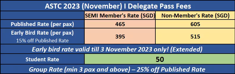
*Above rates are quoted in Singapore Dollars (SGD) and are subjected to 8% GST.
*Above rates are inclusive of coffee/tea breaks and luncheon for both days of the conference.
*Student rate is only applicable with a valid student pass.
*Malaysian Companies - HRDC Claimable for ASTC 2023 November (subject to T&C, please contact HRDC for more information).
For HRDC claims, please refer to the following links on the claiming matrix and guidelines:
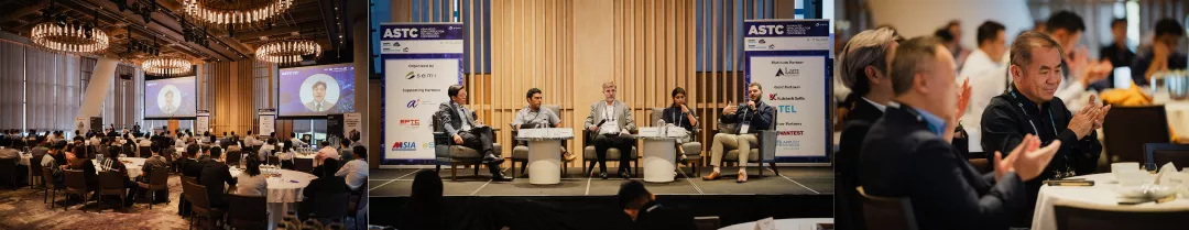
The remarkable advancements in Artificial Intelligence (AI) have spurred extraordinary expansion and creative innovation within the industry. This has paved the way for the SEMI Southeast Asia ASTC Conference & Exhibition of this year, which aims to delve into the Potential of AI and Cybersecurity associated in Manufacturing sector.
Off
Add to Calendar2023-11-16 00:00:002023-11-17 00:00:00Advanced Semiconductor Technology Conference (ASTC) 2023 NovemberThe remarkable advancements in Artificial Intelligence (AI) have spurred extraordinary expansion and creative innovation within the industry. This has paved the way for the SEMI Southeast Asia ASTC Conference & Exhibition of this year, which aims to delve into the Potential of AI and Cybersecurity associated in Manufacturing sector.Andaz Singapore The Glasshouse @ Level 3 5 Fraser Street 189354 SingaporeSEMI.org[email protected]Asia/Singaporepublic
Asia/Singapore
Register Now!
-
10:00 am - 5:00 pm
Off
Add to Calendar2023-07-13 10:00:002023-07-14 17:00:00Thailand Business Summit 2023Bang Kok ThailandSEMI.org[email protected]Asia/Bangkokpublic
Asia/Bangkok
EMG Webinar Push-Pull How Members of the Semiconductor Supply Chain Drive a Sustainable Future
In recent years, sustainability has emerged as a critical aspect of global development, demanding increased attention across industries. The semiconductor industry has a pivotal role to play in promoting environmental responsibility.
In this webinar we will hear the successes, challenges, and ongoing efforts from both a semiconductor device manufacturer and a semiconductor material supplier and how efforts across the supply chain influence each other. Join us as we foster knowledge sharing and collaborations to create a sustainable future for the semiconductor industry and the planet as a whole.
Push & Pull: How the Members of the Semiconductor Supply Chain Drive a Sustainable Future
Brought to you by the EMG Webinar Sub-Committee
10:00 am - 11:00 am
Off
Add to Calendar Disabled
America/Los_Angeles
Register
-
Off
Add to Calendar2023-10-16 00:00:002023-10-18 00:00:00Fundamentals of Product MarketingMilpitas, CA 95035 United StatesSEMI.org[email protected]America/Los_Angelespublic
Experience the industry through Listen, Discuss, See, Touch, and Learn activities and enjoy improved job satisfaction and operational efficiency.
Session 1: The Silicon Chip
"World in a Grain of Sand" Video
Industry chronology
The development of electronics from the thermionic valve to complex ICs
Semiconductor family tree
IC types (logic, memory, microprocessors)
Session 2: Basic Electronics
Introduction to electronics theory
Binary language & ASCII code
Semiconductor materials & their operation
The p-n junction & transistor operation
Boolean algebra & digital logic explained
Session 3: Semiconductor Manufacture
Industry structure
Polysilicon & silicon water production
Wafer fab/front-end process
Back-end (wafer probe, assembly, final test & finishing) operations
"Silicon Chip" video
Session 4: Economics of IC Manufacture
Wafer fab investment trends
Cost structure & cost models
Process yields & manufacturing defects
Die size & cost reduction issues
Back-end cost elements
Typical device costs
Session 5: IC Market Overview
Market segmentation
Company size
Packaging & technology trends
Industry learning curve
Industry cyclicality
Industry dynamics
Market outlook
Session 6: The IT Revolution
Impact of Information Technology
Market trends & industry outlook
Impact of microelectronics
More about the instructor:
Malcolm Penn is the founder of Future Horizons, a leading global semiconductor industry analyst. He has over 50 years’ experience in the semiconductor and electronics industry, from advanced research to manufacturing and applications.
SEMI 673 S. Milpitas Blvd Milpitas, CA95035 United States
Malcolm Penn
Chairman & CEO
Future Horizons
Gain a competitive edge in the Semiconductor Industry by learning how the IC industry works from the science that enables silicon chips to be made from sand to the market fundamentals that drive applications and economics.
This workshop is relevant to technical and non-technical professionals in the semiconductor and IT industry:
Sales, marketing, business development professionals
R&D, engineers, product managers,
Purchasing managers, finance, product planners
Human resources, recruitment and industry training personnel
Government officials, public/private investors
Media, PR and advertising organizations
Attendance is limited to 40 participants.
Silicon Chip Industry Awareness Workshop
A one-day introduction to the Integrated Circuit (IC) Industry technology, manufacturing and markets
9:30 am - 4:00 pm
Off
Add to Calendar2023-05-15 09:30:002023-05-15 16:00:00Silicon Chip Industry Awareness WorkshopGain a competitive edge in the Semiconductor Industry by learning how the IC industry works from the science that enables silicon chips to be made from sand to the market fundamentals that drive applications and economics.
This workshop is relevant to technical and non-technical professionals in the semiconductor and IT industry:
Sales, marketing, business development professionals
R&D, engineers, product managers,
Purchasing managers, finance, product planners
Human resources, recruitment and industry training personnel
Government officials, public/private investors
Media, PR and advertising organizations
Attendance is limited to 40 participants.
SEMI 673 S. Milpitas Blvd Milpitas, CA 95035 United StatesSEMI.org[email protected]America/Los_Angelespublic
America/Los_Angeles
ESD Alliance Export Webinar
This webinar will be recorded. Registrants will receive a link to the recording after the event.
The discussion will help attendees understand why and how governments implement trade controls, what “exports” are and how they take place in different business contexts, and common due diligence methods – such as customer screening – that United States companies use to incorporate regulatory compliance into their business processes. Finally, the discussion will address recent regulatory updates which address current issues such as US-China trade relations and the anticipated effects of those regulations on the US semiconductor design ecosystem.
Following the presentations we will address questions from attendees as time permits.
Meet the Speakers
Ada Loo Group Director and Associate General Counsel, Cadence Design Systems Biography
Ben Kallen Senior Manager, Public Policy & Advocacy SEMI Biography
Marc Coldiron Director of Global Public Policy & Advocacy SEMI Biography
Join us as members of SEMI's Public Policy and Advocacy team will join representatives from Cadence Design Systems to host a webinar focused on export control policy—a topic which is especially relevant to the ESD Alliance given the global reach of the EDA industry. SEMI staff will contextualize export controls within the broader national political landscape and offer their perspective on what EDA companies can expect over the longer term.
ESD Alliance Export Webinar
Navigating Export Controls in EDA
June 11, 2026 | 9–10:30am PT | Virtual
9:00 am - 10:30 am
Off
Add to Calendar2026-06-11 09:00:002026-06-11 10:30:00ESD Alliance Export WebinarJoin us as members of SEMI's Public Policy and Advocacy team will join representatives from Cadence Design Systems to host a webinar focused on export control policy—a topic which is especially relevant to the ESD Alliance given the global reach of the EDA industry. SEMI staff will contextualize export controls within the broader national political landscape and offer their perspective on what EDA companies can expect over the longer term. CA United StatesSEMI.org[email protected]America/Los_Angelespublic
America/Los_Angeles
1
Join us for the annual ESDA CEO/Executive Outlook—
The evening begins at 5:30pm with a networking dinner
Special guest speakers from RISC-V International and SiFive.
Lively panel discussion with influential executives from Breker Verification Systems; D2S; Keysight; PDF Solutions, and Real Intent on the state of the system design industry plus a future industry outlook.
Keysight 5301 Stevens Creek Blvd. Building 5 Santa Clara, CA95051 United States
5:30 pm
-
6:45 pm
Registration/Networking Dinner
6:45 pm
-
6:50 pm
Bob Smith
Executive Director
ESD Alliance
Welcome and Speaker Introductions
6:50 pm
-
7:30 pm
Calista Redmond
CEO
RISC-V International
Jack Kang
SVP of Sales and Business Development
SiFive
Special Guest Speakers
7:30 pm
-
8:30 pm
Bob Smith | Moderator
Executive Director
ESD Alliance
Dave Kelf
CEO
Breker Verification Systems
Aki Fujimura
CEO
D2S
Niels Fache
VP and GM
Keysight
John Kibarian
CEO
PDF Solutions
Prakash Narain
CEO
Real Intent
Moderator & Panelists
Hear panelists from Breker Verification Systems | D2S |Keysight | PDF Solutions | Real Intent discuss the state of the electronic system design industry and their outlook for the coming years.
- Dave Kelf | CEO | Breker Verification Systems
- Aki Fujimura | CEO | D2S
- Niels Fache | VP and GM | Keysight
- John Kibarian | CEO | PDF Solutions
- Prakash Narain | CEO | Real Intent
ESDA CEO/Executive Outlook hosted at Keysight in Santa Clara, CA.
ESD Alliance CEO/Executive Outlook
May 9, 2024
5:30 PM - 8:30 PM
5:30 pm - 8:30 pm
Off
Add to Calendar2024-05-09 17:30:002024-05-09 20:30:00ESD Alliance CEO/Executive OutlookESDA CEO/Executive Outlook hosted at Keysight in Santa Clara, CA. Keysight 5301 Stevens Creek Blvd. Building 5 Santa Clara, CA 95051 United StatesSEMI.org[email protected]America/Los_Angelespublic
America/Los_Angeles
Register Now!