Breakthrough in Semiconductor Lithography Recognized by the American Chemical Society
WILMINGTON, Del., June 10, 2025 – DuPont (NYSE: DD) today announced that 13 of its current and former scientists and engineers have been named 2025 Heroes of Chemistry by the American Chemical Society (ACS) for an innovative program that progressed semiconductor lithography.
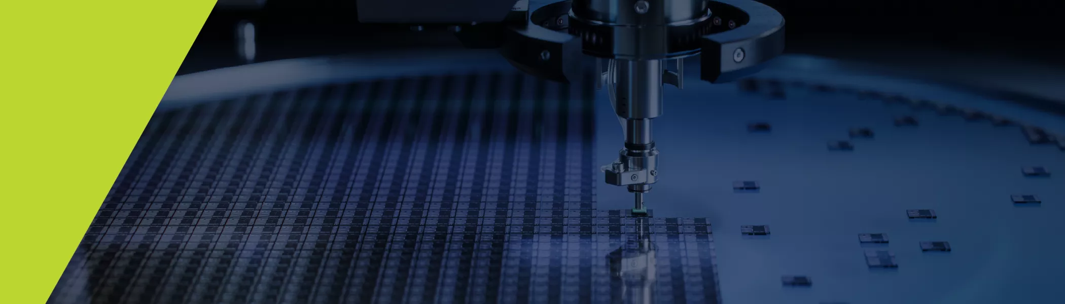
The award recognizes the collaborative development of embedded barrier layer technology, a transformative advancement in 193 nm immersion lithography that significantly improved chip fabrication processes by increasing yield, reducing defects, and enhancing process efficiency. The honored team includes Deyan Wang, Ph.D., Cong Liu, Ph.D., Doris Kang, Ph.D., MingQi Li, Ph.D., Shintaro Yamada, Ph.D., Stefan Caporale, Chengbai Xu, Ph.D., George Barclay, Ph.D., ChunYi Wu, Joon Seok Oh, Li Jia, Jinrong Liu, and Anthony Zampini.
Formulations containing embedded barrier technology have been widely adopted in lithography processes across the global semiconductor industry, supporting advancements for technologies such as artificial intelligence (AI), advanced computing and consumer electronics.
Embedded barrier layer technology addresses key challenges in early immersion lithography such as defectivity and process stability. By integrating barrier functionality directly into the photoresist, fabricators can simplify their lithography processes, with lower materials usage and reduced energy consumption. This advanced technology contributes to improvements in operational efficiency and sustainability for high-volume chip fabrication.
“The introduction of embedded barrier layer technology marked a critical breakthrough innovation for the global semiconductor industry, by extending the capabilities of what is possible with 193 immersion lithography to support the production of advanced, energy-efficient chips,” said Randal King, Vice President of R&D/Technology, Qnity™, DuPont Electronics. “Embedded barrier layer solutions were first implemented over a decade ago and continue to be widely used today. The success of this team demonstrates how materials innovation is powering amazing leaps in technology.”
The ACS Heroes of Chemistry Award is presented annually to industrial scientists whose work has led to the successful development and commercialization of impactful chemistry-based products. The 2025 awardees will be formally recognized at a ceremony in August, as part of the ACS Fall 2025 meeting in Washington, D.C.
About DuPont
DuPont (NYSE: DD) is a global innovation leader with technology-based materials and solutions that help transform industries and everyday life. Our employees apply diverse science and expertise to help customers advance their best ideas and deliver essential innovations in key markets including electronics, transportation, construction, water, healthcare and worker safety. More information about the company, its businesses and solutions can be found at www.dupont.com. Investors can access information included on the Investor Relations section of the website at investors.dupont.com.