microCETI™ supports all laser processes in microLED display manufacturing with up to several orders of magnitude higher transfer rates; multiple system orders already received
Chemnitz, Germany, May 12, 2021—3D-Micromac AG, the industry leader in laser micromachining and roll-to-roll laser systems for the semiconductor, photovoltaic, medical device and electronics markets, today introduced microCETI™—the first laser micromachining platform that supports all laser processes in microLED display manufacturing with the high throughput and precision, and low cost of ownership, needed for volume production requirements.
The microCETI platform is available in three different configurations, enabling cost-effective transfer, lift-off and repair of microLED devices. Its high speed enables the transfer of hundreds of millions of microLEDs per hour without having to apply mechanical forces – up to several orders of magnitude faster than other approaches – while the on-the-fly square-beam laser enables transfer of nearly any shape and size of microLED. 3D-Micromac has already received multiple system orders for the microCETI platform from leading microLED chip manufacturers in North America and Asia for laser lift-off and transfer processing.
A Promising Display Technology Enabled By Laser Micromachining
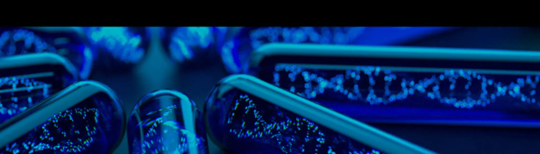
MicroLEDs have the potential to revolutionize the display industry, promising a variety of advantages such as superior viewing angle, high dynamic range with perfect black luminance and high brightness, wide color gamut, fast refresh rates, long lifetime and low power consumption. However, the microLED fabrication process is vastly more complex than LCD and OLED manufacturing, and faces several technical challenges that must be overcome before microLEDs can be readily available in the mass market.
Among these challenges is detaching and transferring the processed microLED chips from the donor or growth (e.g., sapphire) substrate to an intermediate substrate for subsequent testing, allowing the expensive growth substrate to be repurposed for future use. Another challenge is to quickly and precisely transfer the chips to the final glass backplane, which for a typical 4K display involving tens of millions of microLED chips could take hundreds of hours using traditional pick-and-place transfer methods. Technologies are also needed that can detect and repair/replace defective microLEDs during the manufacturing process, since a pixel yield rate of 99.9999 percent is required to produce a full-HD desktop display. The microCETI platform from 3D-Micromac supports all laser processes in microLED display manufacturing, with the ability to address precisely these challenges.
According to Uwe Wagner, CEO of 3D-Micromac, “MicroLEDs have enormous potential for future displays across a wide range of applications and end devices, including indoor and outdoor signage, smart watches, augmented and virtual reality headsets, and automotive heads-up displays. As a leader in laser micromachining, 3D-Micromac has extensive experience applying innovative laser technology to new and emerging applications to support their volume-production requirements. Our new microCETI platform provides a high-throughput, versatile and cost-effective laser micromachining process that is ideally suited for the production of microLEDs. We look forward to working with microLED device and display manufacturers to accelerate the adoption of this exciting and promising display technology.”
The microCETI platform is available in one of three configurations:
• LIFT: unique laser transfer process for nearly every microLED material and shape
• LLO: on-the-fly laser lift-off suitable for customer related microLED material
• REPAIR: Single-die-repair process at every step of the microLED production route
The microCETI platform features a high-precision UV-wavelength laser with high repetition rate and an advanced positioning system for three stages (donor stage, substrate stage and mask stage) and up to 16 axes to transfer every microLED with sub-two-micron positioning accuracy and nanometer-scale repeatability. microCETI supports donor wafer sizes ranging from 50mm (2 inches) up to 200mm (8 inches) as well as intermediate/transfer wafers and backplane substrates up to 350mm x 350mm. In addition to microLEDs, the microCETI platform is also suitable for standard LED and miniLED processing.
Product Availability and Further Information
3D-Micromac is currently accepting orders for the microCETI platform. More information on microCETI, including our latest white paper “Laser technologies for microLED production,” can be found at https://3d-micromac.com/laser-induced-forward-transfer/microceti-lift/.
About 3D-Micromac
Founded in 2002, 3D-Micromac AG is the industry leader in laser micromachining, delivering powerful, user-friendly and leading-edge processes with superior production efficiency. We develop processes, machines and turnkey solutions at the highest technical and technological level. 3D-Micromac systems and services have been successfully implemented in various high-tech industries worldwide including photovoltaic, semiconductor, glass and display industries, micro diagnostics, and medical technology. For more information, visit the company’s website at http://www.3d-micromac.com.