downloadGroupGroupnoun_press release_995423_000000 copyGroupnoun_Feed_96767_000000Group 19noun_pictures_1817522_000000Member company iconResource item iconStore item iconGroup 19Group 19noun_Photo_2085192_000000 Copynoun_presentation_2096081_000000Group 19Group Copy 7noun_webinar_692730_000000Path
Skip to main content
Default Banner Image

United States

SEMI Members:  $49

Use your corporate email address during log in to be recognized as a SEMI Member.

Non-Members:  $99

Students:  Free

Contact Gity Samadi ([email protected]) with a picture of your student ID to receive your discount code. 

Flexible Hybrid Master Classes are offered on many topics!  Visit this page for entire list and links to more detailed information on each one.

Belgium China France Germany Ireland Italy Japan Malaysia Russia Singapore South Korea Taiwan United States Vietnam Watch the Master Class Now FlexTech animation Technical

OVERVIEW

In the last few years, electronics packaging has rightfully emerged from the shadows of CMOS scaling to make a significant impact in high performance and mobile appliance computing.  

In this course, we reviewed the key developments in this paradigm change and the implications these have on Flexible Hybrid Electronics especially the use of bare dielets, fine pitch interconnects and novel substrate materials.

The area of Flexible Hybrid Electronics (FHE) has also developed and is making a significant impact in the area of medical and wellness electronics.  The first generation of these devices have, for most part, adapted Printed Circuit Board (PCB) technology by using thinner PCBs and assembling either thinned or thin packaged “older” generation of chips on to these platforms, typically with coarse printed wiring to connect a small number of such chips.

This approach, while immensely useful to get  the field going, needs to adapt and borrow from the both silicon and advanced packaging technology trends, so that we can advance this trend to the next level. The key paradigm challenges ahead are: scaling  FHE in general – this includes the adoption of dielet (chiplet) technology in more advanced CMOS nodes including edge-AI, higher performance interconnects, flexible high-density energy storage, wireless communication and advanced ergonomics and all of these at lower cost and higher reliability.

This talk addresses the challenges and outline a possible technology roadmap to achieve these goals in the next few years.

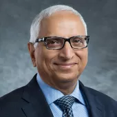
Featured Speaker Biography: Subramanian S. Iyer (Subu) is Distinguished Professor and holds the Charles P. Reames Endowed Chair in the Electrical Engineering Department and a joint appointment in the Materials Science and Engineering Department at the University of California at Los Angeles. He is Director of the Center for Heterogeneous Integration and Performance Scaling (CHIPS). Prior to that he was an IBM Fellow. His key technical contributions have been the development of the world’s first SiGe base HBT, Salicide, electrical fuses, embedded DRAM and 45nm technology node used to make the first generation of truly low power portable devices as well as the first commercial interposer and 3D integrated products. He also was among the first to commercialize bonded SOI for CMOS applications through a start-up called SiBond LLC.

More recently, he has been exploring new packaging paradigms and device innovations that they may enable wafer-scale architectures, in-memory analog compute and medical engineering applications. He has published over 300 papers and holds over 75 patents. He has received several outstanding technical achievements and corporate awards at IBM. He is an IEEE Fellow, an APS Fellow, an iMAPS Fellow and a Distinguished Lecturer of the IEEE EDS and EPS and a member of the Board of Governors of IEEE EPS. He is also a Fellow of the National Academy of Inventors. He is a Distinguished Alumnus of IIT Bombay and received the IEEE Daniel Noble Medal for emerging technologies in 2012 and the 2020 iMAPS Daniel C. Hughes Jr Memorial award.

Read More About Dr. Subramanian Iyer

On-Demand, Online
United States

Subramanian S. Iyer
Subramanian S. Iyer, PhD
Distinguished Chancellor's Professor & Charles P. Reames Endowed Chair
UCLA
- FlexTech Standards

View this Master Class On Demand!  Learn why and how new packaging paradigms like chiplets and dielets are impacting the world of flexible hybrid electronics (FHE) from one of the industry's foremost experts, Dr. Subramanian Iyer of UCLA.  The course explores how these packages are packing such a punch and enabling advanced performance in a much smaller and flexible footprint.

10:00 am - 12:00 pm Off Add to Calendar Disabled
Event format
Promote in calendar
Off

ESPOO, Finland, 13th of April 2021 – Picosun Group has proved to significantly increase the production efficiency of its LED and OLED customers with the PICOSUN® P-300BV ALD system. Recent tests show that a reduced ALD process cycle time and an increased number of wafers deposited with the same film thickness resulted in almost 100% better throughput. A throughput of over 20 000 wafers per month can be reached with a wafer batch of 100 wafers*. At the same time, the process quality in terms of film thickness uniformity has remained on an excellent level (20000 WPM, About Picosun
Picosun provides the most advanced AGILE ALD® (Atomic Layer Deposition) thin film coating solutions for global industries. Picosun’s ALD solutions enable technological leap into the future, with turn-key production processes and unmatched, pioneering expertise in the field – dating back to the invention of the technology itself. Today, PICOSUN® ALD equipment are in daily manufacturing use in numerous leading industries around the world. Picosun is based in Finland, with subsidiaries in Germany, USA, Singapore, Japan, South Korea, China mainland and Taiwan, offices in India and France, and a world-wide sales and support network. Visit www.picosun.com.

More information:
Juhana Kostamo¬
Vice President, Industrial Business Area, Picosun Group
Tel: +358 50 369 9565
Email: [email protected]
Web: www.picosun.com

Industry Reports 15.4% Revenue Growth Overall; Surpasses $3 Billion for Fourth Quarter

MILPITAS, Calif. April 13, 2021 — Electronic System Design (ESD) industry revenue increased by over $1 billion in 2020, marking a new milestone for the industry, the ESD Alliance, a SEMI Technology Community, announced today in the Q4 2020 Electronic Design Market Data report. Revenue increased 15.4% in Q4 2020 to $3,031.5 million, compared to $2,626.3 million in Q4 2019, representing only the fourth time since 2011 that year-over-year growth exceeded 15%. The four-quarter moving average, which compares the most recent four quarters to the prior four quarters, rose by 11.6%, the highest annual growth since 2011 and the second highest in the last 14 years.

“The industry reported a substantial double-digit year-over-year revenue increase for Q4 2020,” said Walden C. Rhines, Executive Sponsor, SEMI Electronic Design Market Data report. “Overall industry revenue surpassed $3 billion for Q4, with increases in all geographic regions. The Computer Aided Engineering (CAE), IC Physical Design and Verification, Semiconductor IP (SIP), and Services categories also reported fourth-quarter growth.”

The companies tracked in the EDMD report employed 48,478 people in Q4 2020, a 6.7% increase over the Q4 2019 headcount of 45,416 and up 3% compared to Q3 2020.

The quarterly EDMD report containing detailed revenue information with the following category and geographic breakdowns.

Revenue by Product and Application Category in Q4 2020

  • CAE revenue increased 9.4% to $956.9 million compared to Q4 2019. The four-quarter CAE moving average also increased 9.4%.
  • IC Physical Design and Verification revenue increased 36.6% to $637.1 million compared to Q4 2019. The four-quarter moving average for the category rose 12.3%.
  • Printed Circuit Board and Multi-Chip Module (PCB and MCM) revenue decreased 0.8% to $292.9 million compared to Q4 2019. The four-quarter moving average for PCB and MCM increased 4.3%.
  • SIP revenue increased 16.9% to $1,052.9 million compared to Q4 2019. The four-quarter SIP moving average grew 17.1%.
  • Services revenue increased 2.2% to $91.6 million compared to Q4 2019. The four-quarter Services moving average decreased 2.4%.

Revenue by Region in Q4 2020

  • The Americas, the largest reporting region by revenue, purchased $1,304 million of Electronic System Design products and services in Q4 2020, a 15.8% increase compared to Q4 2019. The four-quarter moving average for the Americas increased 9.9%.
  • Europe, the Middle East, and Africa (EMEA) revenue increased 2.7%, to $457.2 million compared to Q4 2019. The four-quarter moving average for EMEA grew 6.3%.
  • Japan revenue increased 8% to $228.2 million compared to Q4 2019. The four-quarter moving average for Japan rose 8.2%.
  • Asia Pacific (APAC) revenue increased 23.4% to $1,042 million compared to Q4 2019. The four-quarter moving average for APAC increased 17.1%.

About the EDMD Report

The ESD Alliance Electronic Design Market Data (formerly the Market Statistics Service) reports EDA, IP and services industry revenue data quarterly and is available from SEMI. Both public and private companies contribute data to the report. Each quarterly report is published approximately three months after quarter close. EDMD report data is segmented as follows:

  • Revenue by product category (CAE, IC Physical Design and Verification, Semiconductor IP, PCB/MCM Layout, and Services) including numerous detailed sub-categories
  • Revenue by geographic region (the Americas, Europe Middle East and Africa, Japan, and Asia Pacific)
  • Total employment at participating companies

For information about SEMI market research reports, visit the SEMI Market Research Reports and Databases Catalog.

About the Electronic System Design Alliance

The Electronic System Design (ESD) Alliance, a SEMI Technology Community, is the central voice to communicate and promote the value of the semiconductor design ecosystem as a vital component of the global electronics industry. As an international association of companies providing goods and services throughout the semiconductor design ecosystem, it is a forum to address technical, marketing, economic and legislative issues affecting the entire industry. For more information about the ESD Alliance, visit http://esd-alliance.org.

About SEMI

SEMI® connects more than 2,400 member companies and 1.3 million professionals worldwide to advance the technology and business of electronics design and manufacturing. SEMI members are responsible for the innovations in materials, design, equipment, software, devices, and services that enable smarter, faster, more powerful, and more affordable electronic products. Electronic System Design Alliance (ESD Alliance), FlexTech, the Fab Owners Alliance (FOA) and the MEMS & Sensors Industry Group (MSIG) are SEMI Strategic Association Partners, defined communities within SEMI focused on specific technologies. Visit www.semi.org to learn more, contact one of our worldwide offices, and connect with SEMI on LinkedIn and Twitter.

The information supplied by the ESD Alliance is believed to be accurate and reliable, but the ESD Alliance assumes no responsibility for any errors that may appear in this document. All trademarks and registered trademarks are the property of their respective owners.

Press Contacts

Paul Cohen
ESD Alliance
A SEMI Technology Community
978-769-2106

Jack Taylor
Siemens EDA
512-560-7143

MILPITAS, Calif. – April 13, 2021 – Worldwide sales of semiconductor manufacturing equipment surged 19% from $59.8 billion in 2019 to a new all-time high of $71.2 billion in 2020, SEMI, the industry association representing the global electronics product design and manufacturing supply chain, reported today. The data is now available in the Worldwide Semiconductor Equipment Market Statistics (WWSEMS) Report.

semi logo

For the first time, China claimed the largest market for new semiconductor equipment with sales growth of 39% to $18.72 billion. Sales in Taiwan, the second-largest equipment market, remained flat in 2020 with sales of $17.15 billion after showing strong growth in 2019. Korea registered 61% growth to $16.08 billion to maintain the third position.  Annual spending also increased 21% in Japan and 16% in Europe as both regions are recovering from the contraction in 2019. Receipts in North America decreased 20% in 2020 following three years of consecutive growth.

Global sales of wafer processing equipment rose 19% in 2020, while other front-end segment sales grew 4%. Assembly and packaging showed strong growth across all regions, resulting in a 34% market increase in 2020, while total test equipment sales increased 20%.

Compiled from data submitted by members of SEMI and the Semiconductor Equipment Association of Japan (SEAJ), the Worldwide SEMS Report is a summary of the monthly billings figures for the global semiconductor equipment industry. Equipment categories cover wafer processing, assembly and packaging, test, and other front-end equipment including mask/reticle manufacturing, wafer manufacturing, and fab facilities.
 

Annual Billings by Region in Billions of U.S. Dollars with Year-Over-Year Change Rates 

Region

2020

2019

% Change

China

18.72

13.45

39%

Taiwan

17.15

17.12

0.2%

Korea

16.08

9.97

61%

Japan

7.58

6.27

21%

North America

6.53

8.15

-20%

Europe

2.64

2.28

16%

Rest of the World

2.48

2.52

-1%

Total

71.19

59.75

19%

Source: SEMI (www.semi.org) and SEAJ (www.seaj.or.jp), April 2021


The SEMI Equipment Market Data Subscription (EMDS) provides comprehensive market data for the global semiconductor equipment market. A subscription includes three reports:

  • Monthly SEMI Billings Report, a perspective on equipment market trends
  • Monthly Worldwide Semiconductor Equipment Market Statistics (WWSEMS), a detailed report of semiconductor equipment billings for seven regions and 24 market segments
  • SEMI Semiconductor Equipment Forecast, an outlook for the semiconductor equipment market.

For more information or to subscribe, please contact the SEMI Industry Research and Statistics Group at [email protected]. More information is also available online.


About SEMI
SEMI® connects more than 2,400 member companies and 1.3 million professionals worldwide to advance the technology and business of electronics design and manufacturing. SEMI members are responsible for the innovations in materials, design, equipment, software, devices, and services that enable smarter, faster, more powerful, and more affordable electronic products. Electronic System Design Alliance (ESD Alliance), FlexTech, the Fab Owners Alliance (FOA) and the MEMS & Sensors Industry Group (MSIG) are SEMI Strategic Technology Communities, defined communities within SEMI focused on specific technologies. Visit www.semi.org to learn more, contact one of our worldwide offices, and connect with SEMI on LinkedIn and Twitter.


Association Contact
Michael Hall/SEMI
Phone: 1.408.943.7988
Email: [email protected]

MILPITAS, Calif. – April 6, 2021 – SEMI, the industry association serving the global electronics design and manufacturing supply chain, today announced that it filed comments with the U.S. Department of Commerce in response to its request for public comments regarding risks in the semiconductor manufacturing and advanced packaging supply chain. The comments SEMI submitted provide a summary of the processes, goods and technologies needed for semiconductor production and a host of policy recommendations to strengthen the U.S. semiconductor supply chain and resiliency of the industry.

“Our comments show that just as countless industries depend on semiconductors, semiconductor fabs depend on a complex, global supply chain providing the essential building blocks for semiconductor device manufacturing, from silicon through final test,” said Ajit Manocha, SEMI president and CEO. “Incentives to strengthen the industry must be available to all links within the semiconductor supply chain to minimize potential bottlenecks upstream of chip fabs that could impede the growth of the industry in the United States.”

SEMI recommendations in the comments include:

  • Strong federal manufacturing and research and development incentives for the entire semiconductor supply chain
  • Competitive corporate tax policies
  • Trade policies that open markets and eliminate barriers to trade
  • Harmonized and pragmatic environment, health, and safety regulations
  • Strong workforce development and immigration policies for high-skilled workers
  • Narrowly tailored and multilateral export control policies


About SEMI

SEMI® connects more than 2,400 member companies and 1.3 million professionals worldwide to advance the technology and business of electronics design and manufacturing. SEMI members are responsible for the innovations in materials, design, equipment, software, devices, and services that enable smarter, faster, more powerful, and more affordable electronic products. Electronic System Design Alliance (ESD Alliance), FlexTech, the Fab Owners Alliance (FOA) and the MEMS & Sensors Industry Group (MSIG) are SEMI Strategic Technology Communities, defined communities within SEMI focused on specific technologies. Visit www.semi.org to learn more, contact one of our worldwide offices, and connect with SEMI on LinkedIn and Twitter.

SEMI Contact

Samer Bahou/SEMI
Phone: 1.408.943.7870
Email: [email protected]


Registration

FREE for SEMI | ESDA Members and Non-Members

United States Watch Now Executive looking left Business Executive Featured Speakers

The Executive View—Returning to the Office

Co-Sponsors

SEMI ESD Alliance and Accellera Logo

In a flash last March, employees worked from home, and teleconferencing became a way of life. Executives adopted new guidelines and ensured employees had the proper technology and secure networks to be productive. The workforce adapted, engineers are designing around the world around the clock, and employers are more open to where people work.

Learn about

  • Increased productivity

  • New physical office space setup

  • Using the cloud to overcome technology issues

  • Corporate travel

  • Plus more

Learn why some companies offer more flexibility for employees to work from home at least part of the time. Also, why others may not require new employees to re-locate; perhaps something technology has made easier.

 
KT Moore
MODERATOR
KT Moore
Vice President
Cadence Design Systems
Donna Yasay
Donna Yasay
Senior Leader, Solutions Architecture
Amazon Web Services
Victoria Mitchell
Victoria Mitchell
Vice President, Systems Engineering
Arm
Amin Shokrollahi
Amin Shokrollahi
CEO and Founder
Kandou
Geoff Shippee
Geoffrey Shippee
Vice President
Engineering at Qualcomm Inc.

United States

ESD Alliance

The co-hosts, ESD Alliance and Accellera are looking beyond the pandemic as companies start bringing employees back to the office. A panel of experts explores an executive view and strategies of how the transition from remote work back to the office will unfold.

Off Add to Calendar Disabled America/Los_Angeles
Event format

Registration

Pricing

  • Member: Free
  • Non-Member: $35
United States Register Now Business Featured Speakers

ESD Alliance Webinar

Understanding Export Regulations Affecting the Electronic System Design Ecosystem

The world of export compliance is increasingly complex and perplexing. No one in the electronic system design ecosystem knows this better than Larry Disenhof, ESD Alliance Export Committee Chair and Group Director of Cadence's Export Compliance and Government Relations. 

Join us on Wednesday, September 15, 2021 at 9am PDT to:

  • Hear Larry's perspective and invaluable insights into today's export climate. 
  • Learn how to navigate export regulations.

Larry's expertise on behalf of ESD Alliance's Export Committee is a valued resource for our members. The committee represents the electronic system design ecosystem in Washington, D.C., with agencies overseeing export regulations and other regulatory organizations. Its goal is to educate government agencies about our products and how they are classified in the Commerce Control List to ensure the correct level of export controls are applied. It also serves to educate our members on export and other government regulatory issues affecting our industry and each company's ability to sell and support its products. 

Attendees can expect Larry to present up-to-the-minute and easily understood information about the changeable export landscape, followed by a live Q&A session. 

United States

Larry Disenhof New
ESD Alliance Export Committee Chair
Larry Disenhof
Director, Cadence Export Compliance and Government Relations
Cadence Design Systems, Inc.
ESD Alliance

Join us at the ESD Alliance webinar to hear Larry Disenhof's perspective and invaluable insights into today's export climate and learn how to navigate export regulations. Free registration for members.

9:00 am - 10:00 am Off Add to Calendar 2021-09-15 09:00:00 2021-09-15 10:00:00 ESD Alliance Webinar - Understanding Export Regulations Affecting the Electronic System Design Ecosystem Join us at the ESD Alliance webinar to hear Larry Disenhof's perspective and invaluable insights into today's export climate and learn how to navigate export regulations. Free registration for members. United States SEMI.org [email protected] America/Los_Angeles public America/Los_Angeles
Event format

Registration

Pricing

  • Member: Free
  • Non-Member: $35
United States Register Now CEO Outlook 2021 Update Business Executive Featured Speakers

2021 ESD Alliance CEO Outlook

This year’s informative event, featuring eight prominent industry CEOs, will be conducted as a virtual event.

Ed Sperling, Editor in Chief of Semiconductor Engineering, will moderate this year’s panel, which includes:

  • Arm—Simon Segars
  • Cadence—Lip-Bu Tan
  • IC ManageDean Drako
  • PDF Solutions—John Kibarian
  • Real Intent—Prakash Narain
  • Siemens IC EDAJoseph Sawicki
  • Silvaco—Babak Taheri
  • SynopsysAart de Geus

The panelists will discuss the state of the Electronic System Design industry along with their views of the outlook for the coming years.

United States

Simon Segars, Arm
Simon Segars
CEO, Arm
Lip-Bu Tan, Cadence Design Systems
Lip-Bu Tan
CEO, Cadence Design Systems
Dean Drako, IC Manage
President and CEO, IC Manage
John Kibarian
John Kibarian
CEO, PDF Solutions
Prakash Narain, Real Intent
Prakash Narain
President and CEO, Real Intent
Joe Sawicki, Siemens IC EDA
Joseph Sawicki
Executive Vice President, Siemens IC EDA
Babak Taheri, CEO/CTO, Silvaco
Babak Taheri
CEO/CTO, Silvaco
Aart de Geus, Synopsys
Aart de Geus
Chairman and Co-CEO, Synopsys
ESD Alliance

Join us online May 18 from 2–3pm PDT for the 2021 ESD Alliance CEO Outlook! Free registration for members.

2:00 pm - 3:00 pm Off Add to Calendar 2021-05-18 14:00:00 2021-05-18 15:00:00 ESD Alliance CEO Outlook Join us online May 18 from 2–3pm PDT for the 2021 ESD Alliance CEO Outlook! Free registration for members. United States SEMI.org [email protected] America/Los_Angeles public America/Los_Angeles
Event format

YES (Yield Engineering Systems, Inc.), a preferred supplier of process equipment for the semiconductor advanced packaging, life sciences and display markets, today announced that it will deliver another VertaCure™ XP, the latest version of its flagship VertaCure vacuum curing system, to Winstek Semiconductor Co., Ltd., one of the leading testing and bump houses in Taiwan. The system will be utilized for advanced packaging mass production processes such as copper pillar and WLP to support growth driven by 5G applications, cloud servers and data centers. Winstek received its first VertaCure XP in September of 2020; this repeat order is expected to be delivered in the 2nd quarter of 2021, in order to serve growing market demand.

“The VertaCure XP system’s enhanced capabilities make it especially well-suited for the demands of ‘Beyond Moore’ advanced packaging, and its ability to handle both 200 mm and 300 mm wafers is ideal for our WLCSP application,” said Cheng-Che Tsou, Director of Bumping Engineering at Winstek.

“This follow-on order validates the technology leadership and economic value associated with YES solutions,” said Alex Chow, Asia Sales President & General Manager at YES. “The VertaCure XP’s low vacuum curing environment reduces polyimide curing process time by more than 30%, and its outgassing performance has proven far superior to that of atmospheric ovens. This significant process time reduction in the PVD degas chamber improves both CoO and throughput, not only at the curing process step but also from a process integration prospective,” added Chow. “We greatly value our strong relationship with this strategic customer and look forward to supporting their capacity expansion efforts."

“We have shipped several VertaCure XP systems over the past year, with strong interest from relatively new customers such as Winstek as well as from longtime users of YES systems,” said Rezwan Lateef, President of YES. “We are pleased to have been able to demonstrate the VertaCure XP’s superior film performance and overall value during Winstek’s evaluation process. It has been very gratifying to see the growth of YES in Taiwan extending to this key customer.”

About YES
YES (Yield Engineering Systems, Inc.) is a leading manufacturer of high-tech, cost-effective equipment for transforming surfaces, materials and interfaces. The company’s product lines include vacuum cure systems, chemical vapor deposition (CVD) systems, and plasma etching tools used for precise surface modification and thin-film coating of semiconductor wafers, semiconductor and MEMS devices, biosensors and medical substrates. With YES, customers ranging from startups to Fortune 100 companies can create and volume-produce products in a wide range of markets, including Advanced Packaging, MEMS, Augmented Reality/Virtual Reality and Life Sciences. YES is headquartered in Fremont, California, with a growing presence globally. For more information, please visit https://yieldengineering.com.

About Winstek
One of Taiwan’s leading wafer bumping and testing providers, Winstek Semiconductor Co., Ltd. was founded in 2000 and has offered automated solder bumping since 2005. Applications include 200 mm and 300 mm WLCSP, 300 mm Cu pillar, and others. Winstek's customers range from major corporations to smaller innovators, with end-market products ranging from communications to computers to consumer products. For more information, please visit https://www.winstek.com.tw

United States
Highlighted content

Online
United States

Standards

Automated Test Equipment (ATE) North America TC Chapter Meeting

Date: Tuesday, May 4

Time: 8:00 AM – 10:00 AM Pacific Time

Location: Online via Web Conference


AGENDA

(subject to change) 

Last updated: April 3, 2021 


NOTE: 

Standards meetings are open to all, but you must be a SEMI Standards Program Member to attend. 

If you are not a Member, please register for the International SEMI Standards Program and start making a big contribution to the industry’s progress, complete an application form today! 

Questions? Contact your local staff coordinator: Click here 

8:00 am - 10:00 am Off Add to Calendar 2021-05-04 08:00:00 2021-05-04 10:00:00 ATE North America TC Chapter Meeting Automated Test Equipment (ATE) North America TC Chapter Meeting Date: Tuesday, May 4 Time: 8:00 AM – 10:00 AM Pacific Time Location: Online via Web Conference   AGENDA (subject to change)  Last updated: April 3, 2021    NOTE:  Standards meetings are open to all, but you must be a SEMI Standards Program Member to attend.  If you are not a Member, please register for the International SEMI Standards Program and start making a big contribution to the industry’s progress, complete an application form today!  Questions? Contact your local staff coordinator: Click here  Online United States SEMI.org [email protected] America/Los_Angeles public