The semiconductor industry is entering an era of deep interdependence, rapid innovation, and growing complexity. Breakthroughs in AI accelerators, advanced lithography, heterogeneous integration, and next-generation computing rely on globally distributed ecosystems of suppliers, governments, research institutions, and manufacturers. Yet intelligence systems remain fragmented, limiting visibility and slowing coordinated responses to disruptions and market shifts.
This webinar introduces Co-Intelligence™, a new model that connects intelligence across organizations—not just within them—to enable shared context, collective situational awareness, and coordinated decision-making.
We will also explore Conductor™, a platform designed to operationalize ecosystem-level intelligence by integrating signals across stakeholders and enabling faster, more aligned responses to industry challenges.
Attendees will gain:
A comprehensive view of Co-Intelligence™, the intelligence model for complex semiconductor ecosystems
Access to key insights from an industry leader
An exclusive inside look at the Conductor™ platform
Front-row access to the launch of a new era for the semiconductor industry and invitations to join the emerging network
Agenda:
Welcome & Introductions - Setting the Stage for Co-Intelligence™ – 5 minutes
Keynote – 10 minutes
Roundtable discussion - 10 minutes
Conductor™ Demo – 20 minutes
Q&A – 10 minutes
Session Closes – 5 minutes
Keynote Speaker
I-Ting Fang Department Manager AI for business intelligence TSMC
Bio: I-Ting Fang is a Department Manager at TSMC's Corporate Planning Organization — the “brain” for balancing demand, supply, and capacity planning. She leads teams building intelligence platforms that monitor supply chain health, assess market demand, and track potential events impacting the semiconductor industry and TSMC.
Panelists
Bettina Weiss Chief of Staff & Corporate Strategy SEMI
Sharon Su Director of Strategic Supplier Partnership Dell Technologies
Semiconductor supply chain innovation and orchestration at scale now requires collective intelligence and ecosystem coordination. Join this webinar to explore Co-Intelligence™ and get an exclusive preview of the Conductor™ platform to improve visibility and resilience.
Choose your session:
9-10am CST, April 9 // 6-7pm PDT, April 8 [Register Now]
9-10am PDT, April 10(pre-recorded keynote with live Q&A) [Register Now]
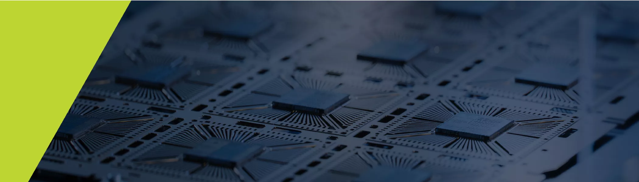
Co-Intelligence™: The New Architecture of Semiconductor Ecosystems
Webinar | Global Sessions
Off
Add to Calendar2026-04-08 00:00:002026-04-10 00:00:00Co-Intelligence™: The New Architecture of Semiconductor EcosystemsSemiconductor supply chain innovation and orchestration at scale now requires collective intelligence and ecosystem coordination. Join this webinar to explore Co-Intelligence™ and get an exclusive preview of the Conductor™ platform to improve visibility and resilience.Choose your session:9-10am CST, April 9 // 6-7pm PDT, April 8 [Register Now] 6-7pm CST // 12-1pm CEST, April 9 [Register Now]9-10am PDT, April 10 (pre-recorded keynote with live Q&A) [Register Now]United StatesSEMI.org[email protected]America/Los_Angelespublic
America/Los_Angeles
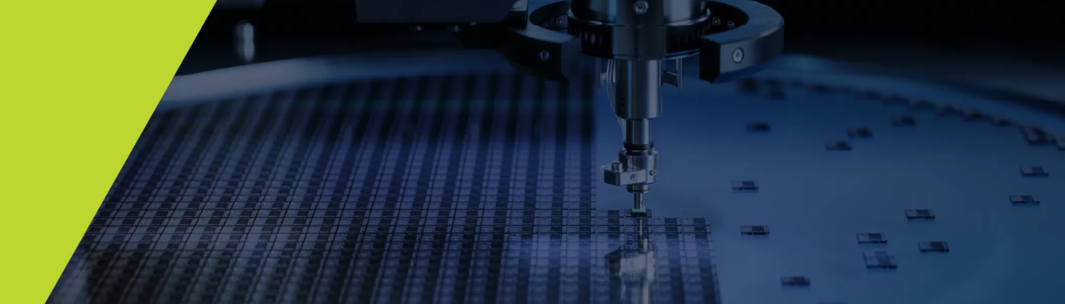
Digital Twin is a virtual representation of the structure, context, and behavior of physical systems or a process, with a live link to a physical system serving as a key enabler for predictive and data-driven optimization. In Printed and Flexible Hybrid Electronics (FHE), manufacturing involves multiple interdependent variables—different printing technologies, inks, substrates, and process conditions—each introducing its own complexity. In practice, additional challenges such as equipment drift, batch-to-batch variations, and environmental fluctuations further impact process consistency and yield. Changing a process or transferring it between tools is often difficult, as each setup is highly customized and sensitive to local conditions. To address these challenges, Digital Twin frameworks connect data from design, fabrication, and metrology into continuously learning digital models. They enable early detection of process drifts, virtual experimentation for process development, and data-driven optimization that reduces time, cost, and waste.
This course introduces Digital Twin frameworks for FHE, focusing on Deep Neural Network (DNN)-based predictive models. Participants will learn how to integrate design, fabrication, and metrology data into continuously learning virtual twins that detect process drifts, enable virtual experimentation, and optimize manufacturing. The program covers the full workflow—from image processing and virtual metrology to AI model training, validation, and hyperparameter tuning—using real datasets. A hands-on “Build Your Own Digital Twin” module in Google Colab will provide practical experience in training and refining models for printed electronics applications, equipping attendees with both theoretical insight and applied skills for process optimization and performance prediction.
ABOUT THE SPEAKER
Benyamin Davaji, PhD Benyamin Davaji is an Assistant Professor in the Department of Electrical and Computer Engineering at Northeastern University, Boston, Massachusetts, where his research centers on integrated microsystems for sensing and computation using mechanical waves. His work spans acoustic and ultrasound transducers, biointerfaces, and microcalorimetry, with a strong emphasis on data-guided nanofabrication, advanced semiconductor device manufacturing, and interdisciplinary approaches to microsystem design and manufacturing. He earned his Ph.D. in Electrical and Computer Engineering from Marquette University in 2016 and completed a postdoctoral appointment at Cornell University.
Join us for a Master Class with Benyamin Davaji, PhD, as he introduces Digital Twin frameworks for Printed and Flexible Hybrid Electronics, demonstrating how AI- and DNN-based models integrate design, fabrication, and metrology data along with printing technologies to detect process drift, enable virtual experimentation, and optimize manufacturing performance. Participants gain hands-on experience building continuously learning digital twins to reduce variability, cost, and time to optimization.
Digital Twins for Printed Electronics: How Can AI Learn FHE Printing?
Flexible Electronics Master Class #29
10:00 am - 12:00 pm
Off
Add to Calendar2026-06-10 10:00:002026-06-10 12:00:00FEMC#29 Digital Twins for Printed Electronics: How Can AI Learn FHE Printing?Join us for a Master Class with Benyamin Davaji, PhD, as he introduces Digital Twin frameworks for Printed and Flexible Hybrid Electronics, demonstrating how AI- and DNN-based models integrate design, fabrication, and metrology data along with printing technologies to detect process drift, enable virtual experimentation, and optimize manufacturing performance. Participants gain hands-on experience building continuously learning digital twins to reduce variability, cost, and time to optimization. United StatesSEMI.org[email protected]America/Los_Angelespublic
America/Los_Angeles
REGISTER NOW
This course provides a practical introduction to atomic layer deposition, an essential technique in semiconductor manufacturing. You'll learn about ALD foundational concepts, including growth, advantages, measurements, and more, chemical precursors for use in ALD, selected ALD processes, area-selective deposition, and atomic layer etching. Overall, the applications and chemistry used in semiconductor processing, as they relate to ALD and ALE, are heavily discussed.
Who Should Attend
This course is intended for both manufacturing and R&D know-how in IC packaging professionals, including but not limited to:
Engeineers
Managers
Process Engineers
R&D Engineers
Sales and Application Engineers who supply packaging materials and tools
Learning Objectives
Understanding foundational concepts of ALD.
Describe chemical precursors for ALD applications.
Identify selected ALD processes and their associated films and materials.
Explain area-selective deposition (ASD), and its uses.
Describe Atomic Layer Etching (ALE) concepts and understand it's relationship to ALD.
Important Information
Note that only the person who registered will receive a certificate of completion. This virtual training will not be recorded. Attendees must be present to access the course knowledge.
Can't find the training link on the day of? After you register, you will receive the link to the live training via the email address you provided. In addition, you will receive email reminders about 24 hours in advance and an hour before with the same link. Please keep these emails on hand to access the training on time. If you do not see any confirmation emails, please check your junk/spam folders before contacting SEMI U for support.
Discover how atomic-scale precision is revolutionizing semiconductor manufacturing with Atomic Layer Deposition (ALD) and Etching (ALE). Course topics include ALD foundational concepts, Chemical Precursors and Processes, and Advanced ALD Techniques.
Pricing
Early Bird Pricing $100 off
Members: $845 $745
Non-Members: $945 $845
* Group pricing for 20+ attendees: $9900 Any questions, please contact [email protected]
Fundamentals of ALD, ALE and Precursors Chemistries
Virtual Training - Americas/EU
7:30 am - 11:30 am
Off
Add to Calendar Disabled
America/Los_Angeles
Register Now
This workshop reviews the needs of the packaging solution to meet the demand for digitalization through the artificial intelligent and Internet-of-things from urbanization, sustainability to industry. The course provides an overview of the fabrication process of IC carriers of leadframe, ceramics, substrate and flex and how they have to evolve to meet the heterogeneous integration. With these foundations, various stacking and integration technologies through wirebonding, flip chip and 3D interconnect from interconnect to system level will be shared. Packaging innovation of TSV, fan-in, fan-out wafer level packaging and its challenges will also be shared for chiplet and heterogeneous integration. It ends off by sharing the embedded technologies and embedded multi-die interconnect bridge for chiplet and heterogeneous integration.
The course looks into the R&D development as well as the dynamics changes of heterogeneous integration technologies in the Semiconductor packaging arena. This workshop curates the technologies development to date and provides the necessary information for professionals in the manufacturing and R&D environment to perform their tasks.
Who Should Attend
This course is intended for both manufacturing and R&D know-how in IC packaging professionals, including but not limited to:
Directors
Managers
Process Engineers
R&D Engineers
Sales and Application Engineers who supply packaging materials and tools
Learning Objectives
Understand why chiplet and heterogeneous integration for advanced packaging
Review of IC carriers
Summarize 3D and TSV for Chiplet and Heterogeneous Integration
Explain Fan-in and Fan-out wafer-level packaging for chiplet and heterogeneous integration
Describe chiplet, embedded, and embedded multi-die interconnect beam for chiplet and glass substrate for heterogenous integration
See what previous course participants had to say about this training!
"All the necessary information are neatly fitted into a few slides prepared by Dr. Lee"
"I found the review of the material between sessions and the slides to follow along with to be the most beneficial aspects of the training."
"Much thanks to Dr. Lee & SEMI University for giving me a chance to study all my unclear items in the past."
Important Information
Note that only the person who registered will receive a certificate of completion. This virtual training will not be recorded. Attendees must be present to access course knowledge.
Can't find the training link day of? After you register, you will receive the link to the live training via the email address you provided. In addition, you will receive email reminders about 24 hours in an advance and an hour before with the same link. Please keep these emails on hand to access the trainings on time. If you do not see any confirmation emails, please check your junk/spam folders before contacting SEMI U for support.
Chiplet and heterogeneous integration of packaging has been embraced as the next revolutionary innovation to meet the quest of size, cost, and performance for packaging. The technologies are seen as another disruptive technology to bring devices into a package by integrating the various Multi-chip module (MCM), 3D packaging, Through Silicon Via (TSV), and Fan-out wafer level packaging (Fo-WLP) technologies into a system in the package for applications. Chiplet, EMIB, and glass substrate will also be shared in this course.
Pricing
Members: $599
Non-Members: $649
* For group orders with 10+ attendees, and for Students/Veterans discounted pricing, please contact [email protected].
Chiplet and Heterogeneous Integration for Microelectronics Packaging
Virtual Training - Asia
8:30 am - 5:00 pm
Off
Add to Calendar2026-06-30 08:30:002026-06-30 17:00:00Chiplet and Heterogeneous Integration for Microelectronics Packaging (Asia) Chiplet and heterogeneous integration of packaging has been embraced as the next revolutionary innovation to meet the quest of size, cost, and performance for packaging. The technologies are seen as another disruptive technology to bring devices into a package by integrating the various Multi-chip module (MCM), 3D packaging, Through Silicon Via (TSV), and Fan-out wafer level packaging (Fo-WLP) technologies into a system in the package for applications. Chiplet, EMIB, and glass substrate will also be shared in this course. PricingMembers: $599Non-Members: $649* For group orders with 10+ attendees, and for Students/Veterans discounted pricing, please contact [email protected]. SingaporeSEMI.org[email protected]Asia/Singaporepublic
Asia/Singapore
Register Now
This course offers a solid foundation in semiconductor manufacturing, from basic concepts to advanced techniques, providing practical insights into the tools, processes, and technologies driving the industry.
Learning Objectives
Gain a comprehensive understanding of the semiconductor industry and manufacturing process, design, and eco-system of the semiconductor industry
Understand the jargon, tools, and materials used in the design and fabrication of an integrated chip
Effectively be able to communicate semiconductor manufacturing concepts with other associates and industry professionals
Course Topics
Basic Electronics and Microelectronics: Definitions of essential electronic terms/concepts and introduction to microelectronics and integrated circuits
Process Nodes: Process nodes and their impact on device performance and cost
Device Physics and Transistor Operation: Principles of device operation and transistor functionality
Crystal Growth and Wafer Preparation: Crystal growth techniques and wafer preparation processes
Advanced Transistor Technologies: FDSOI, FinFETs, and Gate-All-Around (GAA) transistors and their impact on device performance
Circuit Design and Layout: Introduction to circuit design, layout techniques, and tools
Wafer Processing: Mask Making and Lithography: Techniques and materials used in mask making and various lithographic methods (DUV, Immersion, EUV)
Clean Room Environments: Importance of clean rooms in semiconductor manufacturing and contamination issues
Etching and Cleaning Processes: Plasma and wet etching processes
Ion Implantation and Diffusion Techniques: Methods for doping and controlling diffusion in semiconductor fabrication
Deposition Techniques: RTP, CVD, ALD, and ALE techniques and their effect on device performance
Electroplating and Sputtering: Metal deposition techniques used in manufacturing
Packaging and Testing: Techniques such as wire bonding, die stacking, flip chip, and chiplets packaging, semiconductor testing processes
Metrology and Measurement Tools: Tools and methods used for precision measurement in semiconductor manufacturing
Semiconductor Industry Ecosystem: The major players in the industry
Who Should Attend
Anyone interested in understanding semiconductor manufacturing, including new employees, professionals in related industries, and those seeking to broaden their knowledge of the field.
See what course participants had to say about this course!
"The expansive width of coverage with sufficient depth; well curated, relevant information with live references, and the open style of delivery which made the course more of a sharing than a lecture, was enjoyable."
"Denny's knowledge and ability to explain things in simplified ways was awesome!"
"I really enjoyed going over the topics and watching the in-depth videos. I also liked how we received the slide information prior to the class."
"The range of topics was perfect for an intro course."
"Denny did a great job explaining complex topics. The opportunity to ask questions directly was beneficial for the entire class. If a question couldn't be answered immediately, it was addressed by the next break at the latest."
"Thank you very much for the informative course. I appreciate the in-depth and in-detail insight in all aspects of Semiconductor Manufacturing!"
Important Information
Note that only the person who registered will receive a certificate of completion. This virtual training will not be recorded. Attendees must be present to access course knowledge.
Can't find the training link day of? After you register, you will receive the link to the live training via the email address you provided. In addition, you will receive email reminders about 24 hours in an advance and an hour before with the same link. Please keep these emails on hand to access the trainings on time. If you do not see any confirmation emails, please check your junk/spam folders before contacting SEMI U for support.
Gain a comprehensive understanding of the semiconductor industry and the integrated circuit (IC) manufacturing process. This course is designed for new personnel in the field or anyone seeking a well-rounded knowledge of the tools, materials, and terminology used in semiconductor manufacturing.
Pricing
Early Bird Special - $100 off
Members:$995 $895
Non-Members: $1095 $995
* Group pricing for up to 20+ attendees: $12,900 Any questions, please contact [email protected]
Overview of Semiconductor Manufacturing
Virtual Training - Europe
8:00 am - 4:30 pm
Off
Add to Calendar2026-05-27 08:00:002026-05-28 16:30:00Overview of Semiconductor Manufacturing (Europe) Gain a comprehensive understanding of the semiconductor industry and the integrated circuit (IC) manufacturing process. This course is designed for new personnel in the field or anyone seeking a well-rounded knowledge of the tools, materials, and terminology used in semiconductor manufacturing.PricingEarly Bird Special - $100 off Members: $995 $895Non-Members: $1095 $995* Group pricing for up to 20+ attendees: $12,900Any questions, please contact [email protected]GermanySEMI.org[email protected]Europe/Berlinpublic
Europe/Berlin
Register Now
Standards meetings are open to all, but you must be a SEMI Standards Program Member to attend.
If you are not a Member, please register for the International SEMI Standards Program and start making a big contribution to the industry’s progress, complete an application form today!
1:00 pm - 2:00 pm
Off
Add to Calendar2026-03-20 13:00:002026-03-20 14:00:00Traceability NA TC Chapter Meeting 2026Traceability NA TC Chapter Meeting Time:Friday, March 20, 20261:00-2:00 PM Pacificvia Web Conference AGENDA (subject to change)Last updated: March 4, 2026 NOTE:Standards meetings are open to all, but you must be a SEMI Standards Program Member to attend.If you are not a Member, please register for the International SEMI Standards Program and start making a big contribution to the industry’s progress, complete an application form today!United StatesSEMI.org[email protected]America/Los_Angelespublic
America/Los_Angeles
Contact
Michelle Sun Coordinator, International Standards Operations
SEMI Sustainability, in collaboration with STX Group, hosted a webinar on Internal Carbon Pricing (ICP) for the semiconductor value chain. The session was anchored in a new industry report developed with input from members of SEMI’s Carbon Pricing Workgroup and will feature speakers from ASML, Delta Electronics, and Lam Research. The webinar highlighted the 5 key steps in creating and implementing your own ICP plan, and understand the process, its benefits and the opportunities offered.
The presentations explored key insights from the report alongside SEMI member perspectives, with speakers sharing practical examples and lessons learned—from early exploration to applied approaches—across the semiconductor value chain.
Internal Carbon Pricing Webinar for the Semicondcutor Value Chain
U.S. National Strategic Plan for Advanced Manufacturing: Virtual Town Hall for Semiconductor Manufacturing Inputs
Join us for a town hall event designed for semiconductor experts to help shape the future of federal research and development in advanced manufacturing. Participants will share insights to help define the priorities for the 2026–2030 National Strategic Plan for Advanced Manufacturing, which guides Federal efforts to enhance the competitiveness of U.S. manufacturing.
The plan is revised every four years to provide new federal priorities in advanced manufacturing research and development, aiming to create jobs, boost economic growth across various sectors, and strengthen national security. This town hall session augments an online Request for Information (RFI), enabling participants to share their views and catalyze deeper input into priority areas.
The White House Office of Science and Technology Policy has posted the complete set of questions in the Federal RegisterHERE.
The National Science and Technology Council’s Subcommittee on Advanced Manufacturing will manage the RFI process, and the NIST Office of Advanced Manufacturing will collect and analyze the information.
Register and tune in on Tuesday, March 17, 2026 at 11am PT / 2pm ET!
Webinar—11am PT / 2pm ET United States
March 17, 2026 | 11am PT / 2pm ET
Ben Kallen
Sr. Manager, Public Policy & Advocacy,
SEMI
Opening Remarks
Robert Rudnitsky, PhD
Division Chief, Strategy and Planning Division,
National Institute of Standards and Technology (NIST)
2026-2030 National Strategic Plan for Advanced Manufacturing
• Importance of U.S. Manufacturing
• Current - Background on 2022-2026 National Strategic Plan
• Future - Stakeholder RFI on 2026-2030 National Strategic Plan
Audience Input on RFI
Join us for a town hall event designed for semiconductor experts to help shape the future of federal research and development in advanced manufacturing.
U.S. National Strategic Plan for Advanced Manufacturing
Virtual Town Hall for Semiconductor Manufacturing Inputs
March 17, 2026
11am PT / 2pm ET
Off
Add to Calendar2026-03-17 00:00:002026-03-17 00:00:00U.S. National Strategic Plan for Advanced Manufacturing: Virtual Town Hall for Semiconductor Manufacturing InputsJoin us for a town hall event designed for semiconductor experts to help shape the future of federal research and development in advanced manufacturing. Webinar—11am PT / 2pm ET United StatesSEMI.org[email protected]America/New_Yorkpublic
America/New_York
The semiconductor industry stands at a generational inflection point with national economic and security priorities converging to define the role of semiconductors for the future. Engaging with lawmakers and policymakers in Washington, DC on trade policy, tariffs, and export controls is of critical importance for the semiconductor and microelectronics industry. If companies do not engage, policy decisions move forward without industry input, which can create missed opportunities and unnecessary risk.
Join us for this expert panel to hear practical guidance and learn how you can ensure your voice is heard by key decision makers.
Navigating the federal policy landscape can seem daunting. Join SEMI Public Policy & Advocacy for an introduction to advocacy with leading firms K&L Gates, Holland & Knight, and Arnold & Porter as featured presenters. These top DC firms will share a concise advocacy and government affairs “101” on trade, tariff, and export control issues as well as an overview of their services and expertise in Washington, DC.
2:30 pm - 3:30 pm
Off
Add to Calendar2026-02-11 14:30:002026-02-11 15:30:00Washington, DC 101: Trade & Export Controls & Semiconductor Policy Insights Webinar - February 11, 2026Navigating the federal policy landscape can seem daunting. Join SEMI Public Policy & Advocacy for an introduction to advocacy with leading firms K&L Gates, Holland & Knight, and Arnold & Porter as featured presenters. These top DC firms will share a concise advocacy and government affairs “101” on trade, tariff, and export control issues as well as an overview of their services and expertise in Washington, DC.DC United StatesSEMI.org[email protected]America/New_Yorkpublic
America/New_York
This interactive course provides a practical, comprehensive overview of the semiconductor industry, with an emphasis on real-world applications, production processes, and the critical roles within semiconductor manufacturing. Attendees will gain insights into the global semiconductor value chain, from initial design and development to final product shipment, and explore how semiconductors power essential technologies in automotive, AI, and healthcare. The course covers emerging trends such as sustainable manufacturing, data-driven operations, and advanced node technology. Participants will also delve into key performance indicators (KPIs) for fab operations, R&D, and product development, and discover career paths and skill requirements within this dynamic industry.
Through engaging discussions, case studies, and hands-on exercises, participants will gain knowledge that can be immediately applied to their roles, empowering them to better understand semiconductor manufacturing’s impact and contribute to their organization’s success.
Learning Objectives
Identify key applications of semiconductors across industries
Map the semiconductor value chain from design to shipment
Gain understanding of smart manufacturing and resource-efficient production
Interpret KPIs for fab operations, product development, and R&D
Understand key roles and skills within the semiconductor industry
Who Should Attend
This course is ideal for industry newcomers, career changers, recent graduates, technical professionals from related fields, business leaders, and educators seeking a practical, comprehensive understanding of semiconductor applications, processes, roles, and industry dynamics.
Industry Newcomers: Individuals new to the semiconductor field who need a comprehensive overview of applications, production processes, and key roles.
Early- and Mid-Career Semiconductor Employees: Current employees seeking to deepen their understanding of the semiconductor value chain, industry challenges, and emerging trends.
Career Changers and Recent Graduates: Those entering the semiconductor industry or recent graduates looking for insights into industry roles and required skills.
Professionals from Related Fields: Technical professionals in areas like automotive, medical devices, consumer electronics, or engineering who want to understand semiconductor applications and manufacturing.
Managers and Business Leaders: Leaders in strategy, business development, or operations who need to understand semiconductor production dynamics, KPIs, and sustainability to enhance profitability and competition.
Educators and Trainers: Instructors teaching semiconductor technology who want a practical, industry-focused course structure.
Course Topics
Introduction to Semiconductor Applications and Market Impact
Semiconductor Value Chain: From Design to Shipment
Smart Manufacturing and Technology Evolution
Fab Operations and Facility Layout
Key Performance Indicators for Semiconductor Functions
Quality Assurance and Continuous Improvement
Workforce Roles and Skills in Semiconductor Manufacturing
Note that only the person who registered will receive a certificate of completion. This virtual training will not be recorded. Attendees must be present to access course knowledge.
Can't find the training link day of? After you register, you will receive the link to the live training via the email address you provided. In addition, you will receive email reminders about 24 hours in an advance and an hour before with the same link. Please keep these emails on hand to access the trainings on time. If you do not see any confirmation emails, please check your junk/spam folders before contacting SEMI U for support.
Interested in learning about the semiconductor ecosystem as a whole? This course introduces you to the basics of semiconductors, applications of semiconductors, front-end and back-end processing, fabrication facilities, process control and yield management, jobs and roles within the semiconductor industry, and what life is like working in a fab. Great for anyone seeking an understanding of an overview of the industry.
Pricing
Members: $249
Non-Members: $299
* For group orders with 10+ attendees, please contact [email protected].
Semiconductor Ecosystem Overview
Virtual Training - Americas & EU
8:00 am - 12:00 pm
Off
Add to Calendar2026-05-19 08:00:002026-05-19 12:00:00Semiconductor Ecosystem Overview (Americas & EU) Interested in learning about the semiconductor ecosystem as a whole? This course introduces you to the basics of semiconductors, applications of semiconductors, front-end and back-end processing, fabrication facilities, process control and yield management, jobs and roles within the semiconductor industry, and what life is like working in a fab. Great for anyone seeking an understanding of an overview of the industry. PricingMembers: $249Non-Members: $299* For group orders with 10+ attendees, please contact [email protected].United StatesSEMI.org[email protected]America/Los_Angelespublic
America/Los_Angeles
Register Now