downloadGroupGroupnoun_press release_995423_000000 copyGroupnoun_Feed_96767_000000Group 19noun_pictures_1817522_000000Member company iconResource item iconStore item iconGroup 19Group 19noun_Photo_2085192_000000 Copynoun_presentation_2096081_000000Group 19Group Copy 7noun_webinar_692730_000000Path
Skip to main content
Default Banner Image

Virtual

United States Plasma Etching, ALE, & Rie Training

Course Description

The instructor discusses the applied aspects of plasma-assisted etching from a general point of view. The emphasis is on mechanistic understanding. The etching of Si and its compounds is covered in detail. The chemistries used in the etching of other technology-related materials such as Al, organics, and III-V compounds are summarized. Other topics presented include selectivity, loading, ARDE and feature scale problems, damage, and issues associated with high-density plasma RIE. A section on plasma diagnostics and ion-beam based etching methods is briefly discussed. 

Learning Objectives

  • Understand the fundamentals of dry etching and the basic concepts of plasma etching
  • Understand the physics of rf glow discharges (both high and low density)
  • Understand the surface science aspects of RIE including the role of energetic ions
  • Recognize the factors which influence etching anisotropy
  • Define the steps of plasma-surface chemistry leading to etching

Topics Covered

  • Fluorocarbon plasma etching of Si and its compounds
  • Selectivity, loading effects, and aspect ratio dependent etching
  • Uniformity of etching, damage, feature charging issues, and particles
  • Etching of other materials (Al, organics, III-V compounds, etc)
  • Plasma diagnostics such as optical emission spectroscopy with actinometry, mass spectrometry and laser-induced fluorescence
  • Issues in high density plasma etching, wall effects, and ion beam-based methods
  • Deep Reactive Ion Etching (DRIE)
  • Applications and processing etching using ALE
  • End point detection

Who Should Attend

This course is intended for scientists, technicians and others working with or interested in the dry etching of materials in reactive gas glow discharges, particularly those who do not have extensive experience in the field. 
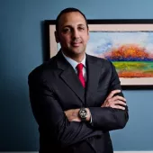
Instructor

Richard Beaudry

PT International, LLC

Instructor Bio
 

Testimonials

See what previous course participants had to say about this training!

  • "Instructors' Process and Hardware knowledge were impressive."
  • "I finally gained a clear understanding of the RIE process."
  • "The instructor had a very good knowledge of the content."
  • "I had a great time to learn fundamental concepts of plasma etching course from SEMI."

Important Information

Note that only the person who registered will receive a certificate of completion. This virtual training will not be recorded. Attendees must be present to access course knowledge. 

Can't find the training link day of? After you register, you will receive the link to the live training via the email address you provided. In addition, you will receive email reminders about 24 hours in an advance and an hour before with the same link. Please keep these emails on hand to access the trainings on time. If you do not see any confirmation emails, please check your junk/spam folders before contacting SEMI U for support.

United States

- SEMI U

This course discusses the fundamentals of plasma assisted phenomena and reactive ion etching (RIE) processes. The emphasis is on the physical and chemical processes that determine the consequences of a reactive gas plasma/surface interaction. The role of energetic ions as encountered in RIE systems is discussed in detail and the factors which influence anisotropy of etching are highlighted. Plasma-assisted etching equipment is described including capacitively coupled, inductively coupled and wave-generated plasmas sources. 

Pricing
  • Members: $845
  • Non-Members: $945

* For group orders with 10+ attendees, and for Students/Veterans discounted pricing, please contact [email protected].

8:00 am - 12:00 pm Off Add to Calendar 2025-07-23 08:00:00 2025-07-24 12:00:00 Plasma Etching, ALE, & RIE (Virtual Training, US & EU) This course discusses the fundamentals of plasma assisted phenomena and reactive ion etching (RIE) processes. The emphasis is on the physical and chemical processes that determine the consequences of a reactive gas plasma/surface interaction. The role of energetic ions as encountered in RIE systems is discussed in detail and the factors which influence anisotropy of etching are highlighted. Plasma-assisted etching equipment is described including capacitively coupled, inductively coupled and wave-generated plasmas sources. PricingMembers: $845Non-Members: $945* For group orders with 10+ attendees, and for Students/Veterans discounted pricing, please contact [email protected]. United States SEMI.org [email protected] America/Los_Angeles public America/Los_Angeles Sold Out
Event format
Promote in calendar
Off
United States Image Training

Course Description

This course offers a solid foundation in semiconductor manufacturing, from basic concepts to advanced techniques, providing practical insights into the tools, processes, and technologies driving the industry.

Learning Objectives

  • Gain a comprehensive understanding of the semiconductor industry and manufacturing process, design, and eco-system of the semiconductor industry
  • Understand the jargon, tools, and materials used in the design and fabrication of an integrated chip
  • Effectively be able to communicate semiconductor manufacturing concepts with other associates and industry professionals

Course Topics

  • Basic Electronics and Microelectronics: Definitions of essential electronic terms/concepts and introduction to microelectronics and integrated circuits
  • Process Nodes: Process nodes and their impact on device performance and cost
  • Device Physics and Transistor Operation: Principles of device operation and transistor functionality
  • Crystal Growth and Wafer Preparation: Crystal growth techniques and wafer preparation processes
  • Advanced Transistor Technologies: FDSOI, FinFETs, and Gate-All-Around (GAA) transistors and their impact on device performance
  • Circuit Design and Layout: Introduction to circuit design, layout techniques, and tools
  • Wafer Processing:
    • Mask Making and Lithography: Techniques and materials used in mask making and various lithographic methods (DUV, Immersion, EUV)
    • Clean Room Environments: Importance of clean rooms in semiconductor manufacturing and contamination issues
    • Etching and Cleaning Processes: Plasma and wet etching processes
    • Ion Implantation and Diffusion Techniques: Methods for doping and controlling diffusion in semiconductor fabrication
    • Deposition Techniques: RTP, CVD, ALD, and ALE techniques and their effect on device performance
    • Electroplating and Sputtering: Metal deposition techniques used in manufacturing
    • Packaging and Testing: Techniques such as wire bonding, die stacking, flip chip, and chiplets packaging, semiconductor testing processes
    • Metrology and Measurement Tools: Tools and methods used for precision measurement in semiconductor manufacturing
  • Semiconductor Industry Ecosystem: The major players in the industry 

Who Should Attend

Anyone interested in understanding semiconductor manufacturing, including new employees, professionals in related industries, and those seeking to broaden their knowledge of the field.


Instructor

Denny Frye 

PT International, LLC

Instructor Bio

Testimonials 

See what course participants had to say about this course!

  • "The expansive width of coverage with sufficient depth; well curated, relevant information with live references, and the open style of delivery which made the course more of a sharing than a lecture, was enjoyable."
  • "Denny's knowledge and ability to explain things in simplified ways was awesome!"
  • "I really enjoyed going over the topics and watching the in-depth videos. I also liked how we received the slide information prior to the class."
  • "The range of topics was perfect for an intro course."
  • "Denny did a great job explaining complex topics. The opportunity to ask questions directly was beneficial for the entire class. If a question couldn't be answered immediately, it was addressed by the next break at the latest."
  • "Thank you very much for the informative course. I appreciate the in-depth and in-detail insight in all aspects of Semiconductor Manufacturing!"

Important Information

Note that only the person who registered will receive a certificate of completion. This virtual training will not be recorded. Attendees must be present to access course knowledge. 

Can't find the training link day of? After you register, you will receive the link to the live training via the email address you provided. In addition, you will receive email reminders about 24 hours in an advance and an hour before with the same link. Please keep these emails on hand to access the trainings on time. If you do not see any confirmation emails, please check your junk/spam folders before contacting SEMI U for support.

United States

- SEMI U

Gain a comprehensive understanding of the semiconductor industry and the integrated circuit (IC) manufacturing process. This course is designed for new personnel in the field or anyone seeking a well-rounded knowledge of the tools, materials, and terminology used in semiconductor manufacturing.

Pricing
  • Members: $995
  • Non-Members: $1,095

* For group orders with 10+ attendees, and for Students/Veterans discounted pricing, please contact [email protected].

7:30 am - 3:00 pm Off Add to Calendar 2025-08-26 07:30:00 2025-08-27 15:00:00 Overview of Semiconductor Manufacturing (Virtual Training, Americas) Gain a comprehensive understanding of the semiconductor industry and the integrated circuit (IC) manufacturing process. This course is designed for new personnel in the field or anyone seeking a well-rounded knowledge of the tools, materials, and terminology used in semiconductor manufacturing.PricingMembers: $995Non-Members: $1,095* For group orders with 10+ attendees, and for Students/Veterans discounted pricing, please contact [email protected]. United States SEMI.org [email protected] America/Los_Angeles public America/Los_Angeles Sold Out
Event format
Promote in calendar
Off
Belgium France Germany Ireland Italy Understanding Semiconductor Technology and Business (EU) Training

Course Description

The first part of the course provides a brief overview of semiconductor design and fabrication steps, encompassing IC design techniques, all wafer processing steps, assembly, and packaging. It delves into semiconductor jargon in laypeople terms, and various substrate types such as Si, SiGe, FDSOI, GaAs, SiC, GaN. Additionally, it discusses different types of transistors like pMOS, nMOS, Bipolar, BiCMOS, CMOS, FinFets, and GAA and their evolution and what applications they are used in.
 
The second part of the course focuses on semiconductor business aspects such as silicon economics, wafer processing costs, semiconductor revenue forecasts, driving forces in the industry, top semiconductor IDMs, market competitors based on market share, OEMs, foundries, top tool vendors, and Fabless companies.  Addresses the fastest-growing semiconductor markets based on geographic locations and applications, identifies semiconductor competitors/customers, and discusses major semiconductor markets like Automotive, PC, Mobile, Memory, Wireless, Cell phones, Consumer, Gaming, AI, IoT, Digital TV, Radio, Automotive, MEMS, and Emerging Technology & Impact on Industry.

Learning Objectives

  • Understand the fundamental principles and theories semiconductor technology.
  • Communicate with other associates and understand wafer processing steps.
  • Understand semiconductor business aspects such as silicon economics, wafer processing costs, semiconductor revenue forecasts, driving forces in the industry, top semiconductor IDMs, market competitors based on market share, OEMs, foundries, top tool vendors, and Fabless companies.
  • Review the semiconductor eco-system as it relates to design and fabrication of a semiconductor device.
  • Gain knowledge of major semiconductor markets like Automotive, PC, Mobile, Memory, Wireless, Cell phones, Consumer, Gaming, AI, IoT, Automotive, MEMS, and Emerging Technology & Impact on Industry.
  • Demonstrate effective communication skills through written reports, presentations, and discussions related to semiconductor subjects.
  • Collaborate effectively with peers in group projects or discussions regarding semiconductor subjects.
  • Analyze and evaluate research literature in semiconductor technology.
  • Develop critical thinking and problem-solving skills applicable to semiconductor technology.

Who Should Attend

This course is suitable for anyone seeking a better understanding of the semiconductor industry, market leaders, terminology, business, and the semiconductor ecosystem.

Instructor

Denny Frye 

PT International, LLC

Instructor Bio
 

Important Information

Note that only the person who registered will receive a certificate of completion. This virtual training will not be recorded. Attendees must be present to access course knowledge. 

Can't find the training link day of? After you register, you will receive the link to the live training via the email address you provided. In addition, you will receive email reminders about 24 hours in an advance and an hour before with the same link. Please keep these emails on hand to access the trainings on time. If you do not see any confirmation emails, please check your junk/spam folders before contacting SEMI U for support. 

Germany

SEMI U

Embark on a journey through semiconductor design, manufacturing, and business in this illuminating course. Explore IC design techniques, transistor evolution, and market dynamics. Delve into substrate types and industry economics, discovering the fastest-growing markets and key players shaping the semiconductor landscape.

Pricing
  • Members: $845
  • Non-Members: $945

* For group orders with 10+ attendees, and for Students/Veterans discounted pricing, please contact [email protected].

9:30 am - 5:00 pm Off Add to Calendar 2025-07-28 09:30:00 2025-07-28 17:00:00 Understanding Semiconductor Technology and Business (Virtual Training, Europe) Embark on a journey through semiconductor design, manufacturing, and business in this illuminating course. Explore IC design techniques, transistor evolution, and market dynamics. Delve into substrate types and industry economics, discovering the fastest-growing markets and key players shaping the semiconductor landscape.PricingMembers: $845Non-Members: $945* For group orders with 10+ attendees, and for Students/Veterans discounted pricing, please contact [email protected]. Germany SEMI.org [email protected] Europe/Brussels public Europe/Brussels Sold Out
Event format
Promote in calendar
Off
China India Japan Malaysia Singapore South Korea Taiwan United States Vietnam (Asia) Understanding, July Training

Course Description

This course offers a solid foundation in semiconductor manufacturing, from basic concepts to advanced techniques, providing practical insights into the tools, processes, and technologies driving the industry.

Learning Objectives

  • Gain a comprehensive understanding of the semiconductor industry and manufacturing process, design, and eco-system of the semiconductor industry
  • Understand the jargon, tools, and materials used in the design and fabrication of an integrated chip
  • Effectively be able to communicate semiconductor manufacturing concepts with other associates and industry professionals

Course Topics

  • Basic Electronics and Microelectronics: Definitions of essential electronic terms/concepts and introduction to microelectronics and integrated circuits
  • Process Nodes: Process nodes and their impact on device performance and cost
  • Device Physics and Transistor Operation: Principles of device operation and transistor functionality
  • Crystal Growth and Wafer Preparation: Crystal growth techniques and wafer preparation processes
  • Advanced Transistor Technologies: FDSOI, FinFETs, and Gate-All-Around (GAA) transistors and their impact on device performance
  • Circuit Design and Layout: Introduction to circuit design, layout techniques, and tools
  • Wafer Processing:
    • Mask Making and Lithography: Techniques and materials used in mask making and various lithographic methods (DUV, Immersion, EUV)
    • Clean Room Environments: Importance of clean rooms in semiconductor manufacturing and contamination issues
    • Etching and Cleaning Processes: Plasma and wet etching processes
    • Ion Implantation and Diffusion Techniques: Methods for doping and controlling diffusion in semiconductor fabrication
    • Deposition Techniques: RTP, CVD, ALD, and ALE techniques and their effect on device performance
    • Electroplating and Sputtering: Metal deposition techniques used in manufacturing
    • Packaging and Testing: Techniques such as wire bonding, die stacking, flip chip, and chiplets packaging, semiconductor testing processes
    • Metrology and Measurement Tools: Tools and methods used for precision measurement in semiconductor manufacturing
  • Semiconductor Industry Ecosystem: The major players in the industry 

Who Should Attend

Anyone interested in understanding semiconductor manufacturing, including new employees, professionals in related industries, and those seeking to broaden their knowledge of the field.


Instructor

Denny Frye 

PT International, LLC

Instructor Bio

Important Information

Note that only the person who registered will receive a certificate of completion. This virtual training will not be recorded. Attendees must be present to access course knowledge. 

Can't find the training link day of? After you register, you will receive the link to the live training via the email address you provided. In addition, you will receive email reminders about 24 hours in an advance and an hour before with the same link. Please keep these emails on hand to access the trainings on time. If you do not see any confirmation emails, please check your junk/spam folders before contacting SEMI U for support.

Singapore

- SEMI U

Gain a comprehensive understanding of the semiconductor industry and the integrated circuit (IC) manufacturing process. This course is designed for new personnel in the field or anyone seeking a well-rounded knowledge of the tools, materials, and terminology used in semiconductor manufacturing.

Pricing
  • Members: $895
  • Non-Members: $995

* For group orders with 10+ attendees, and for Students/Veterans discounted pricing, please contact [email protected].

9:00 am - 4:30 pm Off Add to Calendar 2025-07-17 09:00:00 2025-07-18 16:30:00 Overview of Semiconductor Manufacturing (Virtual Training, Asia) Gain a comprehensive understanding of the semiconductor industry and the integrated circuit (IC) manufacturing process. This course is designed for new personnel in the field or anyone seeking a well-rounded knowledge of the tools, materials, and terminology used in semiconductor manufacturing.PricingMembers: $895Non-Members: $995* For group orders with 10+ attendees, and for Students/Veterans discounted pricing, please contact [email protected]. Singapore SEMI.org [email protected] Asia/Singapore public Asia/Singapore Sold Out
Event format
Promote in calendar
Off
China India Japan Malaysia Singapore South Korea Taiwan Vietnam Understanding Semiconductor Technology and Business (Asia) Training

Course Description

The first part of the course provides a brief overview of semiconductor design and fabrication steps, encompassing IC design techniques, all wafer processing steps, assembly, and packaging. It delves into semiconductor jargon in laypeople terms, and various substrate types such as Si, SiGe, FDSOI, GaAs, SiC, GaN. Additionally, it discusses different types of transistors like pMOS, nMOS, Bipolar, BiCMOS, CMOS, FinFets, and GAA and their evolution and what applications they are used in.
 
The second part of the course focuses on semiconductor business aspects such as silicon economics, wafer processing costs, semiconductor revenue forecasts, driving forces in the industry, top semiconductor IDMs, market competitors based on market share, OEMs, foundries, top tool vendors, and Fabless companies.  Addresses the fastest-growing semiconductor markets based on geographic locations and applications, identifies semiconductor competitors/customers, and discusses major semiconductor markets like Automotive, PC, Mobile, Memory, Wireless, Cell phones, Consumer, Gaming, AI, IoT, Digital TV, Radio, Automotive, MEMS, and Emerging Technology & Impact on Industry.

Learning Objectives

  • Understand the fundamental principles and theories semiconductor technology.
  • Communicate with other associates and understand wafer processing steps.
  • Understand semiconductor business aspects such as silicon economics, wafer processing costs, semiconductor revenue forecasts, driving forces in the industry, top semiconductor IDMs, market competitors based on market share, OEMs, foundries, top tool vendors, and Fabless companies.
  • Review the semiconductor eco-system as it relates to design and fabrication of a semiconductor device.
  • Gain knowledge of major semiconductor markets like Automotive, PC, Mobile, Memory, Wireless, Cell phones, Consumer, Gaming, AI, IoT, Automotive, MEMS, and Emerging Technology & Impact on Industry.
  • Demonstrate effective communication skills through written reports, presentations, and discussions related to semiconductor subjects.
  • Collaborate effectively with peers in group projects or discussions regarding semiconductor subjects.
  • Analyze and evaluate research literature in semiconductor technology.
  • Develop critical thinking and problem-solving skills applicable to semiconductor technology.

Who Should Attend

This course is suitable for anyone seeking a better understanding of the semiconductor industry, market leaders, terminology, business, and the semiconductor ecosystem.

Instructor

Denny Frye 

PT International, LLC

Instructor Bio
 

Important Information

Note that only the person who registered will receive a certificate of completion. This virtual training will not be recorded. Attendees must be present to access course knowledge. 

Can't find the training link day of? After you register, you will receive the link to the live training via the email address you provided. In addition, you will receive email reminders about 24 hours in an advance and an hour before with the same link. Please keep these emails on hand to access the trainings on time. If you do not see any confirmation emails, please check your junk/spam folders before contacting SEMI U for support. 

Singapore

SEMI U

Embark on a journey through semiconductor design, manufacturing, and business in this illuminating course. Explore IC design techniques, transistor evolution, and market dynamics. Delve into substrate types and industry economics, discovering the fastest-growing markets and key players shaping the semiconductor landscape.

Pricing
  • Members: $745
  • Non-Members: $845

* For group orders with 10+ attendees, and for Students/Veterans discounted pricing, please contact [email protected].

9:00 am - 4:30 pm Off Add to Calendar 2025-07-16 09:00:00 2025-07-16 16:30:00 Understanding Semiconductor Technology and Business (Virtual Training, Asia) Embark on a journey through semiconductor design, manufacturing, and business in this illuminating course. Explore IC design techniques, transistor evolution, and market dynamics. Delve into substrate types and industry economics, discovering the fastest-growing markets and key players shaping the semiconductor landscape.PricingMembers: $745Non-Members: $845* For group orders with 10+ attendees, and for Students/Veterans discounted pricing, please contact [email protected]. Singapore SEMI.org [email protected] Asia/Singapore public Asia/Singapore Sold Out
Event format
Promote in calendar
Off
United States
Highlighted content

Due to scheduling conflicts we need to postpone the event and we will announce the rescheduled event when we are able. Thank you for your interest and for more information about Chips & Childcare, please reach out to Michelle Williams at [email protected]. We look forward to welcoming you to the future webinar!

The SEMI Foundation is committed to helping companies address the child care needs of the employees who build and facilitate their fabs.  In partnership with Policy Equity Group, a nationally recognized organization with extensive child care expertise, SEMI has engaged with companies in several states to problem-solve child care issues and identify tailored solutions.  

United States

10:00 am
Michelle Williams
Michelle Williams-Vaden
Executive Director
SEMI Foundation

Welcome: The Importance of Addressing Employee Child Care Needs

10:05 am
Jeffrey Capizzano
Jeffrey Capizzano
CEO
Policy Equity Group

Framing Child Care Challenges for the Semiconductor Industry Employer Supports & Resources

Dahlin cropped
Melissa Dahlin, PhD
Senior Director
Policy Equity Group
10:15 am
Karyn Olsson Cropped
Karyn Olsson
Public Relations
Calumet Technologies

Industry Insights: Evaluating Employee Needs to Identify Child Care Solutions

10:30 am
Andi Zolkiewski TSMC AZ
Andi Zolkiewski, MBA
Human Resources
TSMC AZ

Industry Insights: Identifying Child Care Partnerships Through Child Care Market Analysis

10:45 am - 11:00 am

Q&A

Workforce Development Off Add to Calendar Disabled America/Los_Angeles
Event format

Registration

Member: $49
Non-Member: $99

Registrants will receive the presentation recording and PDFs of Webinar #7.

Taylor Zhao
Manager, Programs & Committees
[email protected]

+
United States REGISTER NOW New - SiC Webinar 7 800x800 Tile Business Technical Training

SiC—Silicon Carbide Webinar #7: 

SiC Planar and Trench MOSFETs: Design, Fabrication, and Key Applications

Silicon Carbide (SiC) MOSFETs exploit the material’s favorable properties, which allow for highly efficient power devices with reduced form-factor and cooling requirements. Having been commercially introduced in 2011, SiC MOSFETs have gone through several generations of improvements and are currently offered in planar and trench configurations by major semiconductor chip manufacturers. This webinar will provide an impartial overview of planar/trench design and fabrication aspects, highlight their key competitive advantages, and provide an independent overview of what real-world converters require in terms of application-specific performance parameters. Exemplary applications to be discussed include aviation, servo drivers, energy storage, and traction drives.


View other webinars in the SiC Series

  • Webinar #1—Silicon Carbide Material Properties, Key Applications, and Fabrication Basics: Making the Transition from Silicon
  • Webinar #2—Non-CMOS Compatible SiC Power Device Fabrication in Volume Si Fabs
  • Webinar #3—Bidirectional SiC and GaN Switch Technology
  • Webinar #4—Understanding SiC Chip Cost, the Impact of Defects, and the Case of Price Parity with Si at the System Level
  • Webinar #5—SiC Edge Termination Technology
  • Webinar #6—Basal Plane Dislocation Defects and the Impact on Device Performance


Meet the Speaker

View David Levett's Biography

View Victor Veliadis's Biography

United States

Victor Veliadis, PowerAmerica
Moderator
Victor Veliadis
Executive Director & CTO
PowerAmerica
David Levett, Power Converter Consulting
David Levett, PhD
Design Engineer
Power Converter Consulting

Join us online for the seventh webinar in the Silicon Carbide Series.

9:00 am - 10:00 am Off Add to Calendar Disabled America/Los_Angeles 1
Event format
Promote in calendar
Off
United States MMRL Tile

Abstract

The successful development of MEMS (Micro-Electro-Mechanical Systems) products requires a structured approach that balances innovation with manufacturability, cost, and time to market. The MEMS Manufacturing Readiness Levels (MMRL) Guide provides a comprehensive framework to navigate this process, from initial concept through high-volume production.

In this webinar, we will explore how MMRL facilitates efficient MEMS development by defining commonly accepted readiness levels, best practices, and key decision points. Attendees will gain insights into:

  • The MMRL framework and its role in MEMS product development
  • Best practices for reducing risks and accelerating time to market
  • Strategies for ensuring performance, quality, and cost targets are met
  • Real-world applications and lessons learned from implementing MMRL

Join us to learn how MMRL can streamline your MEMS development process, improve collaboration, and drive successful product commercialization.


Speakers


Michelle Bourke | Managing Director of Strategic Marketing and Specialty Technologies, Lam Research

Michelle Bourke received her B.Sc. degree in Optoelectronics and Laser Engineering from Heriot-Watt University in Scotland, UK. Subsequently she joined the Defence Evaluation and Research Agency (DERA), where she worked on advanced processing methods for GaAs/AlGaAs optoelectronic devices. In 1997 she entered the semiconductor capital equipment industry as a technologist and has since accrued more than 25 years of experience in semiconductor technology, strategy, and new product development. She is a specialist in fabrication technologies for MEMS, Power Devices, RF Electronics and Optoelectronics.

Michelle is a frequent presenter at leading industry forums and also serves on many committees and industry councils. In November of 2018, she was inducted into the SEMI MEMS and Sensors Industry Group Hall of Fame and in 2020 she was a Silicon Valley YWCA Tribute to Women Honoree. Michelle is currently Chair of the Semi MEMS Manufacturing Working Group, Co-chair of the SEMI MEMs Standards Committee and a Director on the Transducers Research Foundation Board where she is the Chair of Fund Raising and Development Committee.

Michelle joined Lam Research in 2015 and is currently Managing Director of Strategic Marketing in Lam’s Customer Support Business Group.


Mary Ann Maher, SoftMEMS

Mary Ann Maher | CEO, SoftMEMS LLC

Mary Ann Maher is the CEO of SoftMEMS LLC. She received her Ph.D. degree in 1989 from Caltech in the area of semiconductor device modeling. She has held positions at the Swiss Center for Electronics and Microtechnology (CSEM), Tanner Research and MEMSCAP Inc. She founded SoftMEMS LLC in 2004. She has over 30 years of experience in the field of computer aided design for MEMS.


Rob Pugliese | Principal Engineer, HP Inc.

Rob Pugliese is a Principal Engineer at HP Inc. in Corvallis Oregon.  Rob has held several  engineering roles in inkjet printhead development in his 32 years at HP, from etching and deposition engineer to yield improvement, printhead architecture design and life science fluid dispensing, as well as a rotation in engineering management. He is currently working in the MEMS section of the Microfluidics Technology Incubation lab, where he guides development of new microfluidic devices, curates the technology development process, and leads the tooling/capability strategy for the MEMS fab. Rob has a Ph.D. in Chemical Engineering from the University of Massachusetts at Amherst.


Tyler Harrison | Design Engineer, Teledyne MEMS

Dr. Tyler Harrison is the lead Design Engineer at Teledyne MEMS in Edmonton, Canada. His undergraduate background in Computer Engineering led to a PhD program focused on ultrasound and photoacoustic systems design and integration, all at the University of Alberta. After graduating, a postdoctoral position shared between the University of Alberta and Micralyne Inc (now Teledyne MEMS) led to full time MEMS development work in 2016. Since then, he’s filled a variety of Engineering roles helping develop new processes and translate customer concepts to fabricated devices. In his tenure at Teledyne MEMS, he’s led several initiatives to automate and error-proof layout processes, standardize process control monitoring, and use data-driven approaches to improve first-run performance on new devices.


Tim Maloney | Senior Director of Business Development, Polar Semiconductor 

Tim Maloney is the Senior Director of Business Development at Polar Semiconductor in Bloomington, Minnesota. With over 25 years of experience in the semiconductor industry, Tim has led initiatives across process engineering, factory operations, technology transfers, and supply chain management. In his current role, he is instrumental in Polar Semiconductor’s transformation into a U.S.-based open foundry specializing in power and sensor devices. His career includes leadership roles at Motorola Semiconductor, onsemi, Seagate Technology, SkyWater Technology, and Polar Semiconductor. Tim holds a background in Industrial Engineering from the University of Wisconsin-Madison and Arizona State University.

United States

MSIG Standards 8:00 am - 9:00 am Off Add to Calendar 2025-03-12 08:00:00 2025-03-12 09:00:00 New SEMI MEMS Standard: Guide to MEMS Manufacturing Readiness Levels [Webinar] United States SEMI.org [email protected] America/Los_Angeles public America/Los_Angeles Register here
Event format

Join Us

Complete the form below to sign up for our live webinar.

United States REGISTER NOW Greene Tweed 2025 Webinar 690x448 Tile Business Executive

With the world's growing reliance on semiconductor chips, the industry needs a more reliable solution to improve and innovate at a rapid pace while addressing manufacturing challenges such as temperature, chemistry, and mechanical issues. 

One critical equipment in the industry is vacuum Pendulum Valves, a vacuum equipment incorporating plasma that are widely used in the semiconductor manufacturing process. The form, fit and function of these valves pose multiple challenges for the seals required in the valve's assemblies.  Greene Tweed engineers have analyzed the most commonly used pendulum valves and broken down the various sealing challenges and have also created solutions to the challenges. 

Join us to learn about the 6 W's—Who, What, When, Where, Why, & How—of these pendulum valve solutions.

  • Who—Anyone running a vacuum plasma chamber, etch and/or deposition  
  • What—The pendulum valves, specifically the seals in the valve  
  • Where—Every fabricator in the world
  • When—Now, as there are, tens of thousands that are currently operating
  • Why—The prevalent sealing challenges for pendulum valves
  • How—The sealing solutions and how we develop them, and the case study behind it to show in the 'How' part as well 

Join our webinar where Greene Tweed engineers will discuss the most commonly used pendulum valves, the various sealing challenges and solutions to address them.  

United States

Virtual Webinar | Tuesday, March 4, 2025 | Pacific Time

9:00 am
Carmen Quartapella, Greene Tweed
Carmen Quartapella
Senior Engineer, Design & Analysis
Greene Tweed

Register today to join our live webinar in collaboration with Greene Tweed!

9:00 am - 10:00 am Off Add to Calendar Disabled America/Los_Angeles 2
Event format
United States Understanding Semiconductor Technology and Business Training
Highlighted content

Course Description

The first part of the course provides a brief overview of semiconductor design and fabrication steps, encompassing IC design techniques, all wafer processing steps, assembly, and packaging. It delves into semiconductor jargon in laypeople terms, and various substrate types such as Si, SiGe, FDSOI, GaAs, SiC, GaN. Additionally, it discusses different types of transistors like pMOS, nMOS, Bipolar, BiCMOS, CMOS, FinFets, and GAA and their evolution and what applications they are used in.
 
The second part of the course focuses on semiconductor business aspects such as silicon economics, wafer processing costs, semiconductor revenue forecasts, driving forces in the industry, top semiconductor IDMs, market competitors based on market share, OEMs, foundries, top tool vendors, and Fabless companies.  Addresses the fastest-growing semiconductor markets based on geographic locations and applications, identifies semiconductor competitors/customers, and discusses major semiconductor markets like Automotive, PC, Mobile, Memory, Wireless, Cell phones, Consumer, Gaming, AI, IoT, Digital TV, Radio, Automotive, MEMS, and Emerging Technology & Impact on Industry.

Learning Objectives

  • Understand the fundamental principles and theories semiconductor technology.
  • Communicate with other associates and understand wafer processing steps.
  • Understand semiconductor business aspects such as silicon economics, wafer processing costs, semiconductor revenue forecasts, driving forces in the industry, top semiconductor IDMs, market competitors based on market share, OEMs, foundries, top tool vendors, and Fabless companies.
  • Review the semiconductor eco-system as it relates to design and fabrication of a semiconductor device.
  • Gain knowledge of major semiconductor markets like Automotive, PC, Mobile, Memory, Wireless, Cell phones, Consumer, Gaming, AI, IoT, Automotive, MEMS, and Emerging Technology & Impact on Industry.
  • Demonstrate effective communication skills through written reports, presentations, and discussions related to semiconductor subjects.
  • Collaborate effectively with peers in group projects or discussions regarding semiconductor subjects.
  • Analyze and evaluate research literature in semiconductor technology.
  • Develop critical thinking and problem-solving skills applicable to semiconductor technology.

Who Should Attend

This course is suitable for anyone seeking a better understanding of the semiconductor industry, market leaders, terminology, business, and the semiconductor ecosystem.

Instructor

Denny Frye 

PT International, LLC

Instructor Bio
 

Important Information

Note that only the person who registered will receive a certificate of completion. This virtual training will not be recorded. Attendees must be present to access course knowledge. 

Can't find the training link day of? After you register, you will receive the link to the live training via the email address you provided. In addition, you will receive email reminders about 24 hours in an advance and an hour before with the same link. Please keep these emails on hand to access the trainings on time. If you do not see any confirmation emails, please check your junk/spam folders before contacting SEMI U for support. 

United States

SEMI U

Embark on a journey through semiconductor design, manufacturing, and business in this illuminating course. Explore IC design techniques, transistor evolution, and market dynamics. Delve into substrate types and industry economics, discovering the fastest-growing markets and key players shaping the semiconductor landscape.

Pricing
  • Members: $845
  • Non-Members: $945

* For group orders with 10+ attendees, and for Students/Veterans discounted pricing, please contact [email protected].

9:30 am - 5:00 pm Off Add to Calendar 2025-06-02 09:30:00 2025-06-02 17:00:00 Understanding Semiconductor Technology and Business (Virtual Training, US) Embark on a journey through semiconductor design, manufacturing, and business in this illuminating course. Explore IC design techniques, transistor evolution, and market dynamics. Delve into substrate types and industry economics, discovering the fastest-growing markets and key players shaping the semiconductor landscape.PricingMembers: $845Non-Members: $945* For group orders with 10+ attendees, and for Students/Veterans discounted pricing, please contact [email protected]. United States SEMI.org [email protected] America/Los_Angeles public America/Los_Angeles Closed
Event format
Promote in calendar
Off