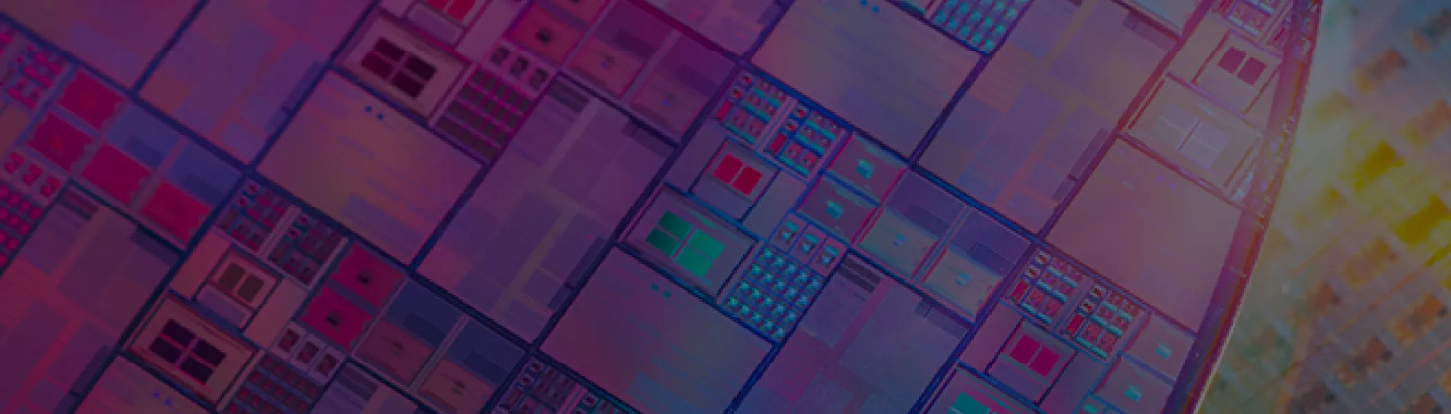
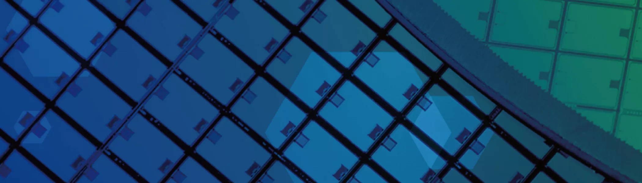
Moore’s Law continues to evolve - dramatically changing the Field Effect Transistor (FET). As FinFETs reach their performance limits, attention is turning to Gate All Around (GAA) architectures based on Horizontal Nanosheet technology. Such a fundamental shift in transistor architecture will create new challenges to processes and materials, presenting opportunities for companies well-positioned for this shift.
In this webinar, SEMI EMG brings experts to explain the technology trends driving the industry adoption of Gate All Around, how the major players are approaching this transition, and the implications this will have on the material supply chain
Gate All Around Transistors - Opportunities Abound
Position yourself for the next chapter of Moore's Law
10:00 am - 11:00 am
Off
Add to Calendar Disabled
America/Los_Angeles
Sponsorships can be tailored to meet your branding and marketing objectives. Become a sponsor and brand your company at the Silicon Valley Virtual Forum.
Contact Shane Poblete, +1.202.847.5983 or Eric Rude, +408.943.7047 to learn about available sponsorship opportunities.
Environmental Sustainability—Semiconductor Industry Challenges
High demand for semiconductor chips is driving significant growth and increased visibility of the industry. At the same time, the world is becoming more environmentally conscious and the topic of sustainability of semiconductor manufacturing is coming to the forefront. This requires the entire semiconductor value chain to concurrently support this growing demand while minimizing waste, toxic chemicals and gas emission to produce these chips.
Join us for a Virtual Webinar on March 18, 2022 as the SEMI Silicon Valley Chapter presents “Environmental Sustainability—Semiconductor Industry Challenges” for a great line-up of industry leaders from their own perspectives.
Silicon on Insulator technology is a very diverse and multi-faceted enabler of semiconductor products. In certain areas if offers performance advantages across a wide dynamic range of leakage and in other areas it enables the use of high voltages in multi-domain designs. It also inherently bring low capacitance which makes it great for ultra-fast switching in RF designs and significantly improved radiation robustness compared to bulk CMOS; it’s easy to see why SOI technology continues to expand in use through-out the industry.
Attend this webinar to see how these advantages are being applied to products in the medical and automotive (and more) application spaces.
CA United States
8:00 am
-
8:10 am
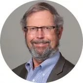
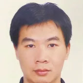
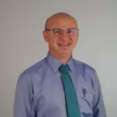
Carlos Mazure
SOI Consortium
Welcome and Introduction
8:10 am
-
8:30 am
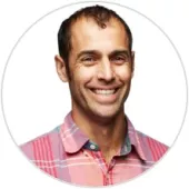
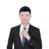
Jon Cheek
Sr. Director, Process Technology Development
NXP Semiconductor
SOI Technology: Enabling Everything from Automotive to 6G
Abstract – The use of Fully-Depleted SOI, FD-SOI, combined with an ultrathin buried oxide create a technology ideally suited for the Internet of Things revolution. FDSOI enables the dynamic modulation of the threshold voltage during operation, not just during the design phase, to open a whole new world of creative product opportunities. One such example is the creation of ultralow leakage embedded SRAM memories which consume so little power that some resulting IoT products can last years on a single household battery. Other versions of SOI Technology with thick buried oxide enable use of 50V to 70V domains on a chip without need of complex isolation schemes. This ability to provide high voltage support along with digital processing is yet another reason SOI is adopted to provided differentiation in product offerings. Each of these approaches will be discussed and shown how it benefits the final products.
8:30 am
-
8:50 am
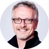
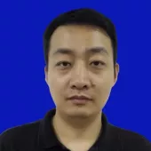
Giulio Ricotti
Design Director & Technical Staff Fellow
ST Microelectronics
BCBD-SOI Technologies and Applications in Ultrasound Imaging and More
Giulio Ricotti – Design Director and Technical Staff Company Fellow - STMicroelectronics
After earning his Electronics Engineering degree, Giulio joined ST in 1994 as a design engineer in their Smart Power (SP) products group. Currently a Design Director and Technical Staff Company Fellow, Giulio has more than 60 patents and has authored 70 publications. Giulio has also been awarded the “Premio dei Premi” in 2009 by the Italian president Giorgio Napolitano for his crucial contribution to innovation with the 4D ultrasound imaging project that is used today all over the world for pregnancy and cardiology screenings.
Join us for the the first in a series of webinars focused on applications of SOI technology, brought to you by the SEMI SOI Consortium. The series will underline the breadth of products that SOI technologies cover.
The first webinar of the series will feature ST Microelectronics and NXP. ST Microelectronics will focus on their BCD-SOI technologies and applications, such as medical ultrasound imaging. NXP will showcase multiple applications of SOI technologies in automotive from power electronics through infotainment.
Latest Trends in SOI-based Microelectronics Applications
8:00 am - 9:00 am
Off
Add to Calendar Disabled
America/Los_Angeles