SEMI Members: $75
Use your corporate email address during log in to be recognized as a SEMI Member.
Non-Members: $149
Students: Free
Contact Basak Ulutas Ozturkler ([email protected]) with a picture of your student ID to receive your discount code.
This comprehensive course will cover the underlying fundamentals, the interrelationship between materials and processes, and the hardware used in printed electronics. The masterclass will also explore how printed electronics can be applied currently in example applications including practical aspects of the technology, its highlights and challenges and scalability. We will also explore emerging new technologies at the cutting edge of FHE, semiconductor packaging, photonics and quantum materials. Throughout the course there will be opportunities for Q/A and discussions and case studies based on participant's interest.
ABOUT THE SPEAKER
J. Devin MacKenzie, PhD
Dr. Devin MacKenzie is the Washington Research Foundation Professor and an Assoc. Prof. of Materials Science and Engineering and Mechanical Engineering at UW. He is also the Technical Director of the Washington Clean Energy Testbeds, a lab that provides open-access to world-class advanced manufacturing and characterization tools for printed optoelectronics, sensors and energy device research and scale-up. Devin also has 25 years of entrepreneurial experience in sustainable materials and manufacturing of semiconductors, optoelectronics and energy devices. Prior to UW he was CEO and co-founder of printed battery company, Imprint Energy (acquired CCL/Avery), Previously, as the CTO of Add-Vision, Inc. (acquired Sumitomo Chemical), Dr. MacKenzie led R&D for roll-to-roll printed flexible OLEDs at Add-Vision with licensing in Europe and Asia. Prior to Add-Vision, he led printed silicon RF device and product engineering at Kovio, Inc. a Si Valley MIT spin-out (acquired Thin Film Electronics). Dr. MacKenzie also co-founded, Plastic Logic, from Cambridge University as a postdoc and subsequently a visiting scientist in Physics at the Cavendish Laboratory. Prior to that he worked at Bell Labs and NASA. Dr. MacKenzie has authored over 240 publications and patents that have been licensed globally and has been cited over 12,900 times in fields ranging from rare earth-doped nitrides to quantum materials. He holds Ph.D, MS, and undergraduate degrees in Materials Science and Engineering from the University of Florida and the Massachusetts Institute of Technology.
United States


Join us for a comprehensive Master Class with Dr. Devin MacKenzie, as he dives into the fundamentals and real-world applications of printed and flexible hybrid electronics (FHE). This session will explore the critical interrelationship between materials, processes, and hardware used in printed electronics, providing a strong foundation for understanding how these systems are designed and manufactured.
Participants will gain insight into current applications of printed electronics, along with practical considerations such as performance, scalability, and manufacturing challenges. The course will also highlight emerging technologies at the forefront of innovation, including advances in FHE, semiconductor packaging, photonics, and quantum materials


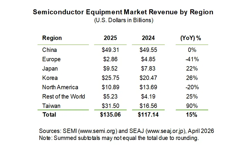
 In 2025, the global front-end semiconductor equipment market posted solid growth, with wafer processing equipment sales increasing 12% and other front-end segments rising 13%. The expansion was driven primarily by continued investment in leading-edge logic and memory capacity, supported by AI-related demand and ongoing node and technology migrations.