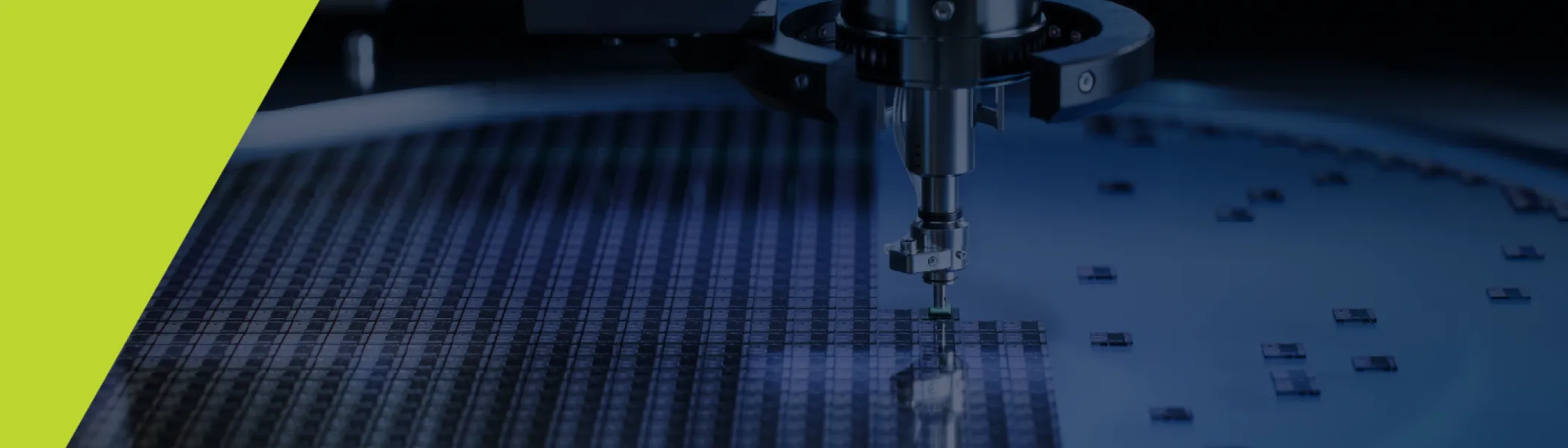
downloadGroupGroupnoun_press release_995423_000000 copyGroupnoun_Feed_96767_000000Group 19noun_pictures_1817522_000000Member company iconResource item iconStore item iconGroup 19Group 19noun_Photo_2085192_000000 Copynoun_presentation_2096081_000000Group 19Group Copy 7noun_webinar_692730_000000Path
Skip to main content
Default Banner Image

United States

Date: May 8, 2026

Location: Drammen, Norway

Board-level and semiconductor test data are often analyzed separately, limiting correlation across the product lifecycle. Linking PCB assembly (PCBA) test results, including in-circuit and functional test, with upstream wafer, sort, and final test data remains difficult, particularly in photonics, advanced packaging, and high-density integration environments. yieldWerx and WATS announce a partnership to bridge this gap in the PCB test and semiconductor manufacturing workflows.

WATS is a test data management platform purpose-built for electronics manufacturers. It captures, standardizes, and analyzes high-volume test data from PCBA (printed circuit board assembly) production environments, including in-circuit test (ICT), functional test, and final test, giving engineers real-time visibility into board-level yield, anomalies, and quality metrics across the production line.

yieldWerx operates at the semiconductor level, connecting data across wafer fabrication, wafer sort, die, and packaged device test. Its enterprise analytics platform enables advanced yield analysis, traceability, and root cause investigation from design through silicon manufacturing.

Together, the platforms address the full product stack. This allows manufacturers to correlate PCBA-level signals with silicon quality data, improving visibility across test stages and enabling more effective analysis of yield and reliability issues.

Customer and industry benefits include:

Real-time PCBA test visibility for faster identification of yield and quality issues

Improved correlation between board-level test results and upstream chip or wafer data

Reduced time spent reconciling data across disconnected systems

Earlier detection of cross-stage patterns impacting yield and reliability

Faster root cause analysis spanning silicon, assembly, and board-level test

Better alignment between electronics manufacturing and semiconductor supply chain

The combined solution supports open architectures, APIs, and flexible deployment models, enabling integration without large-scale system changes.

About yieldWerx

yieldWerx is an enterprise analytics platform connecting data across the semiconductor product lifecycle, from design and wafer fabrication through wafer sort, die, and packaged device test, enabling advanced yield analysis, traceability, and data-driven decision-making across cloud, on-premises, and hybrid environments.

About WATS

WATS is a test data management and analytics platform developed by Virinco, built to collect, standardize, and analyze data from electronics manufacturing test systems. It provides real-time visibility into board-level performance across ICT, functional test, and final test operations, helping engineers monitor yield, detect anomalies, and improve quality at high volume.

Statements from Leadership
"We are excited to partner with yieldWerx. Our customers manufacture complex electronics where board-level test data alone only tells part of the story. By connecting PCBA production test data with yieldWerx's upstream semiconductor intelligence, we can give them a more complete picture of their product quality and yield." -- Tom Lomsdalen, CEO, Wats

“Our customers have been asking for a unified view that links semiconductor yield data with downstream electronics test results, and this partnership delivers exactly that. Together, yieldWerx and WATS empower engineering teams to move faster on root cause analysis, reduce escapes, and make smarter decisions across the entire product lifecycle.” -- Aftkhar Aslam, CEO, yieldWerx

For further information, please visit https://www.yieldWerx.com or https://www.Wats.com/.

Semiconductor industry leader takes the helm to accelerate Beneq’s next phase of growth in atomic layer deposition

Espoo, Finland, 8 May, 2026 – Beneq Oy, the home of atomic layer deposition (ALD), today announced the appointment of Dr. Jason Harrison as Chief Executive Officer. Dr. Harrison succeeds Dr. Tommi Vainio and will lead Beneq into its next phase of growth across semiconductor, optical, and emerging technology markets.

A Strategic Leadership Transition
Beneq enters its next phase of growth from a position of strong commercial momentum. Recent milestones include the qualification of the Beneq Transform® cluster tool for volume production of GaN power and RF filter devices; the introduction of Beneq Transmute™ and Beneq Transform® XP, both engineered for high-volume manufacturing (HVM) of specialty semiconductors; growing adoption of the P-Series for coating critical chamber parts in advanced node devices; and selection of the C2R™ for AR waveguide production in next-generation XR optics.

Against this backdrop, the Board of Directors has determined that the time is right to align executive leadership with the company's evolving strategic priorities. As part of this transition, Dr. Tommi Vainio has decided to step down as CEO to pursue other opportunities. The Board of Directors extends its sincere thanks to Tommi, whose leadership advanced Beneq's technology platform, strengthened its market position in thin film deposition, and guided the company through important stages of its development.

A Proven Leader for a Scaling ALD Business
Dr. Harrison brings extensive global experience across the semiconductor and advanced technology sectors. He holds a Ph.D. in Quantum Chemistry and has built a distinguished career spanning device manufacturing, process development, and equipment solutions, with senior leadership roles at Intel, Lam Research, Veeco, and Applied Materials covering research and development, new product introduction, global account management, and business unit leadership. This combination of technical depth and commercial acumen positions him to scale Beneq’s commercial execution and growth across its global customer base.

Looking Ahead
Under Jason’s leadership, Beneq will accelerate strategic execution across its expanding portfolio, deepen customer engagement across North America, Asia, and Europe, and continue investing in innovative ALD solutions from R&D to HVM to deliver long-term value to customers, employees, and stakeholders.

Dr. Patrick Rabinzohn, Member of the Board of Directors, Beneq, said: “Jason brings the technical depth, the business and account management experience, and the global perspective Beneq needs at this stage of its growth. His academic background and compelling track record across the semiconductor industry positions Jason to build on the momentum the company generated especially.”

Dr. Jason Harrison, Chief Executive Officer, Beneq, added: “Beneq has a strong technology foundation, a talented team, and a growing pipeline of customers in some of the most important markets in semiconductors and optics. I look forward to working with the team to accelerate execution and deliver on the trust our customers place in us.”

About Beneq
Beneq pioneered industrial production of Atomic Layer Deposition (ALD) with the introduction of the first commercial ALD equipment in 1984. Today, Beneq advances ALD adoption and validation with a portfolio that includes the Beneq Transform®, Transform XP, Transform 300, and Transmute™ for specialty semiconductor device fabrication; TFS 200 and TFS 500 for R&D; the P400A, P800, and P1500 batch systems for coating critical semiconductor chamber components and complex part geometries; and spatial ALD platforms such as the C2R™ and roll-to-roll processing equipment. Headquartered in Espoo, Finland, Beneq enables ALD integration from lab to fab for semiconductors, optics, and functional coatings.

Press Contacts
Lie Luo
Head of Marketing
[email protected]

ROSENHEIM, Germany / KUALA LUMPUR, 5 May 2026 — esmo group (esmo), a leading global full-service systems integrator, developer, and supplier of advanced automation solutions for the semiconductor test industry, today announces the debut of its X-change Cart. A dedicated, semi-automated Device Interface Board (DIB) exchange system that enables a complete load board changeover by a single operator in under one minute, the X-change Cart addresses the safety, efficiency, and reliability challenges associated with manual board handling on the semiconductor test floor.

In high-mix semiconductor test environments, load board changeovers are a frequent and operationally significant activity. The reliance on manual handling has long presented challenges around changeover time, operator safety, and the risk of damage to high-value boards.

“Across test floors, we kept seeing the same pattern,” said Josef Weinberger, Head of Business Unit, esmo semicon. “Board changeovers were slow, physically demanding, and too dependent on individual technique. In tight spaces, that's where mistakes happen and time is lost. That observation drove us to build a dedicated solution that makes changeovers fast, repeatable, and manageable by a single operator in under a minute.”

Engineered for the Modern Test Floor

The X-change Cart removes the physical demands and variability of manual board handling from the equation entirely. Through a structured, HMI-controlled process, a single operator can lock, rotate, and transfer a board to the tester within a minute. The ability to carry two boards in a single trip makes that timescale achievable in practice. Thoughtful design details, including a ±180° rotation at the locking mechanism and a ±90° tower swivel, address the real-world constraints of a busy test floor.

Broad compatibility with leading ATE platforms (e.g. Teradyne, Advantest, SPEA and more) facilitates integration into existing multi-vendor environments without reconfiguration, allowing OSATs and IDMs to realise multiple benefits without disruption to their current setup.

For facilities with longer-term automation objectives, an optional configuration allows the interface tower to be mounted onto a customized AGV or AMR, providing a practical upgrade path toward autonomous test floor operations. The modular design further allows additional features to be incorporated as operational requirements evolve.

Weinberger added, “Reliability in production comes down to the details. The gripper head is engineered to perform consistently under real production conditions, with ESD-safe construction ensuring the board is protected at every point of contact. That level of engineering discipline is what makes the difference on a real production floor.”

X-change Cart Key Features

  • Modular DIB exchange system for reliable, error-free board loading and unloading
  • One-person operation — complete board change in under one minute
  • Transports two load boards simultaneously for rapid exchange
  • Full multi-axis rotation: ±180° at locking mechanism | ±180° Y-axis | ±90° Z-axis
  • Compatible with leading ATE platforms — Teradyne, Advantest, SPEA and more
  • Interfaces with test head, prober, DIB-loader, storage rack, and maintenance workbench
  • Tower swivels ±90° for use in narrow corridors and constrained test floor layouts
  • Integrated Human-Machine Interface (HMI), sensor detection, safety hand-brake, and modular battery
  • Optional: fully automated configuration mountable on AGV or AMR

The X-change Cart will be available for live demonstration at the esmo booth throughout SEMICON Southeast Asia 2026. Visit esmo at Booth 2145, Hall 8, Level 2, MITEC Kuala Lumpur from 5–7 May 2026, or contact [email protected] to arrange a meeting or request further information.

United States AI Techniques in Semiconductor MFG Business Executive Technical

Suggested Hotels:

Embassy Suites by Hilton Milpitas Silicon Valley

901 East Calaveras Boulevard

Milpitas, CA 95035

(408) 942-0400


Courtyard by Marriott Milpitas Silicon Valley

1480 Falcon Dr.

Milpitas, CA 95035

(408) 719-1966


Event Sponsors

Sponsorship Opportunities

Enhance your brand with our exclusive sponsorship packages. For details, contact:

Karim Somani
Email: [email protected]

Highlighted content

AI Techniques in Semiconductor Manufacturing

Core Objectives:

This workshop is designed to help participants understand:

  • The real-world deployment, impact, and lessons learned from AI techniques

  • Strategies for building observable and scalable multi-agent workflows

  • The industry transition from restrictive data silos toward autonomous discovery.

  • Methods for achieving tangible business results and automation through diverse AI applications 

We’ve curated a technical agenda featuring Topics such as:

  • Agentic AI

  • Gaussian Process Regression

  • Time Series Modeling

  • Bayesian Optimization

  • And more...

You will walk away with actionable insights on:

  • Yield Enhancement through Edge-Driven Defect Detection and Classification
    • Demonstrates how edge AI leverages real-time sensor and image data—through virtual metrology, anomaly detection, and SPC-integrated feedback loops—to enable early defect detection, classification, and yield optimization.
  • From Prediction to Action: Causal AI for Real-Time Root-Cause Analysis in Semiconductor Manufacturing
    • How causal AI unifies multi-modal fab data into an intelligence layer to move beyond predictive alerts toward rapid root cause identification, prescriptive actions, and continuous improvement—significantly reducing RCA time and improving yield and operational efficiency.

  • From Data Silos to Autonomous Discovery: Agentic AI in Semiconductors
    • Agentic AI in semiconductor workflows as autonomous, decision-making systems (beyond RAG) that orchestrate multi-agent reasoning across complex fab data—requiring robust data foundations, domain-grounded algorithms, SME-driven knowledge (including reasoning traces), and structured evaluation frameworks (agentic harness) to ensure reliable, scalable deployment.

  • Making Sense of Equipment TimeSeries Data: From Signals to Insight
    • Introduces how semiconductor equipment time-series data (sensor signals, traces, run-to-run data) can be processed and modeled to uncover equipment behavior over time, enabling engineers to detect drift, changes, and anomalies for improved monitoring and troubleshooting.
  • Achieving Business Results from Air-gapped Agentic AI Automation in Semiconductor Manufacturing - Lessons from the Field
    • Highlights real-world deployment of agentic AI in fabs, demonstrating how autonomous systems are driving yield, capacity, and operational gains across engineering workflows (FDC, yield, test, maintenance) while navigating constraints like data privacy and legacy integration—along with practical adoption strategies and hands-on use cases.
  • And more...


SEMI HQ
673 S Milpitas Blvd.
Milpitas, CA 95035
United States

Morning, Day 1: December 4, 2024

8:00 am - 9:00 am

Registration & Breakfast​

9:00 am - 12:30 pm

Session #1 - Data Needs for Digital Twins - Data Sources, Integration & Interoperability

This session will explore the critical data requirements for creating and maintaining digital twins. Integrating multi-modal data sources (sensors, enterprise systems, equipment, etc.) that feed into digital twins, ensuring that they accurately reflect their physical counterparts is a minimum necessity. This session will also cover data integration techniques (from various factory systems), and interoperability to support dynamic digital twins.

9:00 am - 9:10 am
Mark da Silva
Mark da Silva​
Senior Director, Smart Manufacturing
SEMI

Welcome Remarks

9:10 am - 9:35 am
Mike Neel
Michael Neel
Director of Marketing
Inficon

Keynote​ - Enabling Autonomous Operations Through Integrated Digital Twins

9:35 am - 10:00 am
Robert Baseman
Robert Baseman
Senior Technical Staff Member
IBM

Semantic Models for Microelectronic Manufacturing & Development

10:00 am - 10:25 am
David McKee
Technology Leader & Managing Partner
Counterpoint Tech/DTC

Journey to Twins: A toolkit for Capabilities & Data to Digital Twins

10:25 am - 10:40 am

Coffee Break - Sponsored by INFICON

Inficon Logo 170x65
10:40 am - 11:05 am
Rad Desiraju
Rad Desiraju
Director, WW Industry Advisory
Microsoft

Overcoming Data Interoperability Challenges for Effective Digital Twins

11:05 am - 11:30 am
Wei Zhao
Wei Zhao
Head of Process Integration
Athinia
Chris Han-Adebekun
Chris Han-Adebekun
VP, Business Development
Athinia

Building Process & Supply Chain Digital Twins through Integrated Data Assets and Secure Data Sharing

11:30 am - 12:30 pm
Dave Henshall
Dave Henshall
Vice President of Business Development and Government Relations
Semiconductor Research Corporation
Chris Ritter
CTO
Idaho National Lab

Special Session - SmartUSA – Semiconductor Digital Twin Manufacturing USA Institute

12:30 pm - 2:00 pm

Lunch

Afternoon, Day 1: December 4, 2024

2:00 pm - 5:00 pm

Session #2 - Data Standards for Digital Twins: Managing Unclean Factory Data

This session will focus on the importance of data standards for digital twins in semiconductor manufacturing, particularly in the context of dealing with unclean factory data. It will explore the challenges associated with unclean data and discuss strategies for cleaning and standardizing to ensure seamless ingestion into digital twins at various levels. Best practices for data validation, transformation, and integration as well as how to implement robust data standards to enhance reliability and accuracy of digital twins.

Sponsored by - Seeq

SEEQ
2:00 pm - 2:25 pm
Dr. Joseph Ervin
Dr. Joseph Ervin
Product Line Head of Semiverse Solutions Group
Lam Research

Keynote - Addressing Future Challenges in the Stochastics Era of Patterning with EUV Dry Resist

New patterning technologies will be needed to advance the device roadmap to 2 nm and beyond. Minimum pitch scaling will be exceptionally difficult to achieve at these advanced nodes, even with EUV patterning. Stochastic effects using wet resists during EUV patterning become problematic at the nanoscale, and can lead to line collapse, bridging, unacceptable line edge roughness (LER) and line width roughness (LWR). These stochastic effects present challenges when optimizing the tradeoffs between EUV resist resolution, dose, sensitivity, line edge / line width roughness, defectivity and cost.
In this talk, we will review the basics of dry resist technology, including dry resist equipment requirements, process flows and process integration modeling. In addition, we will present data that documents the advantages of dry resist technology over wet resist technology, demonstrating superior image quality, scaling and yield. We will conclude the talk by demonstrating a digital twin of the process integration and usage of optimization to achieve improved LER/LWR characteristics.

2:25 pm - 2:50 pm
Alan Weber
Alan Weber
Vice President, New Product Innovations
Cimetrix by PDF Solutions

Charting the Digital Twin Standardization Path: An Iterative Implementation and Abstraction Process

2:50 pm - 3:15 pm
Brett Brimhall
Deloitte

3:15 pm - 3:30 pm

Coffee Break - Sponsored by INFICON

Inficon Logo 170x65
3:30 pm - 3:55 pm
Andres Torres
Andres Torres
Engineer and Key Expert
Siemens

Feature Engineering as the bridge to Semantic Factory Data

3:55 pm - 4:20 pm
Michael Bowcutt
Michael Bowcutt
Director of Sales Engineering for Romaric products at camLine
camLine USA

Control Software Integration with Digital Twins: How Virtual Data Aligns with Physical Reality

4:20 pm - 5:20 pm
Kenneth Smith
Moderator
Kenneth Smith
VP Growth Markets
Seeq
Sean Tropsa
Sean Tropsa
Principal Analytics Engineer
Seeq

Panel: Harmonizing Standards for Semiconductor Digital Twins​ ​

5:30 pm - 7:00 pm

Networking Reception - Sponsored by Sentient Cloud

Sentient Cloud

Morning, Day 2: December 5, 2024

8:00 am - 9:00 am

Registration & Breakfast​

9:00 am - 12:30 pm

Session #3 - Modeling High Complexity Semiconductor Processes

This session will explore the integration of digital twin technology in modeling high complexity semiconductor processes. As the semiconductor industry advances, the need for precise and efficient modeling techniques becomes crucial. Digital Twins offer a transformative approach to simulate and optimizes these processes, though challenges exist. Cases studies and future innovations will also be covered in this session.

9:00 am - 9:05 am
Mark da Silva
Mark da Silva​
Senior Director, Smart Manufacturing
SEMI

Welcome Remarks

9:05 am - 9:30 am
Umesh Kelkar
Umesh Kelkar
Master/Vice President, Semiconductor Products Group
Applied Materials

Keynote: Key Enablers for Semiconductor Equipment and Process Digital Twins: Accelerated Computing (AC), Artificial Intelligence (AI) and Physics Modeling

9:30 am - 9:55 am
Prith Bannerjee
Prith Bannerjee
Chief Technology Officer
Ansys

AI Driven Digital Twins for Semiconductor Manufacturing

9:55 am - 10:20 am
Xi-Wei Lin
Xi-Wei Lin
Executive Director, Applications Engineering
Synopsys

AI and Physics-based Models for Technological Development with High Complexity Semiconductor Processes

10:20 am - 10:45 am

Coffee Break - Sponsored by PhysicsX

PhysicsX
10:45 am - 11:10 am
Amit Lal
Amit Lal
Professor, Cornell University
Cornell
Peter Doerschuk
Peter Doerschuk
Professor
Cornell University
Ben Davaji
Ben Davaji
Assistant Professor
Northeastern University

Digital Twin Flow Using AI/ML Applied to Ferroelectric Memory

11:10 am - 11:35 am
John Maculley
John Maculley
Semiconductor Industry Strategy Consultant
Dassault Systemes

Leveraging Virtual Twins and AI for Enhanced Fabrication Technology Co-Optimization in Semiconductor Manufacturing

11:35 am - 12:30 pm
Pushkar Apte
Strategic Technology Advisor and Global Data-AI Lead
SEMI

Panel Discussion

12:30 pm - 2:00 pm

Lunch - Sponsored by Dassault Systemes

Dassault Systems

Afternoon, Day 2: December 5, 2024

2:00 pm - 5:00 pm

Session #4 - GenAI & AI/ML Role in the Development of Digital Twins - Implementation Strategies for DT

Integrating AI/GenAI & Digital Twins - Explore the cutting-edge integration of Generative AI (GenAI) and Artificial Intelligence/Machine Learning (AI/ML) in the creation and evolution of digital twins. This session will delve into how GenAI & AI/ML technologies are revolutionizing the simulation, prediction, and real-time replication of physical assets in semiconductors through case studies and practical applications. 


2:00 pm - 2:25 pm
Kamaljeet Ghotra
Kamaljeet Ghotra
Senior Director, Go-To Market and Digital Strategy
PDF Solutions

Keynote - Accelerating Digital Twins with Gen AI

The rise of sophisticated AI tools, including generative AI, is revolutionizing the semiconductor industry by enabling the analysis of vast datasets to generate valuable insights. Executives in the sector see generative AI as a transformative force rather than just another tool. They believe it can deliver significant value, particularly in manufacturing, operations, and maintenance, its potential for process and equipment analysis, Predictive maintenance and smart diagnostics.

As fabs adopt smart manufacturing and virtual modeling it is pertinent for digital twins to leverage technologies like generative AI for data generation, Data Synthesis/Augmentation, Real Time Analysis, Model Optimization (AI enhanced physics models) , Rapid Prototyping and Accelerated Design and Development with data-driven model-based learning.

2:25 pm - 2:50 pm
Peter Lendermann
Peter Lendermann
CTO
D-SIMLAB

About Cross-Fertilization between Digital Twins and AI Techniques for Capacity Planning and WIP Flow Optimisation in Semiconductor Fabs​

2:50 pm - 3:15 pm
Kiran Karunakaran
Kiran Karunakaran
Chief Technology Officer
Via Automation

Developing Explainable Digital Twins for the Semiconductor Industry Using GenAI, Knowledge Graphs, and ML Techniques​

3:15 pm - 3:30 pm

Coffee Break - Sponsored by PhysicsX

PhysicsX
3:30 pm - 3:55 pm
Mark Huntington
Mark Huntington
Managing Director of North America
PhysicsX

Real-Time Digital Twins for Semiconductor Manufacturing: Accelerating Multi-Physics Optimization with Physics-Based AI

3:55 pm - 4:20 pm
Becky Kelderman
Becky Kelderman
Solutions Sales Manager
Rockwell Automation

Advancing Industrial Data Architectures & Models for AI in Process Digital Twins

4:20 pm - 5:20 pm
Mithun Kamat
Moderator
Mithun Kamat
Partner
McKinsey

Panel - Rewiring organizations for AI / Digital twin: a business-backed view of successful implementation and challenges in adoption of Digital twins in the semiconductor industry

- Smart MFG


The SEMI Smart Manufacturing Initiative is hosting a two-day workshop titled "AI Techniques in Semiconductor Manufacturing" at SEMI HQ in Milpitas, CA, on August 5–6, 2026. This event is part of a continuing series focused on integrating advanced AI into the semiconductor landscape. The workshop is designed to help participants understand: The real-world deployment, impact, and lessons learned from AI techniques. Strategies for building observable and scalable multi-agent workflows. The industry transition from restrictive data silos toward autonomous discovery. Methods for achieving tangible business results and automation through diverse AI applications.

8:00 am - 5:00 pm Off Add to Calendar 2026-08-05 08:00:00 2026-08-06 17:00:00 AI Techniques in Semiconductor Manufacturing  The SEMI Smart Manufacturing Initiative is hosting a two-day workshop titled "AI Techniques in Semiconductor Manufacturing" at SEMI HQ in Milpitas, CA, on August 5–6, 2026. This event is part of a continuing series focused on integrating advanced AI into the semiconductor landscape. The workshop is designed to help participants understand: The real-world deployment, impact, and lessons learned from AI techniques. Strategies for building observable and scalable multi-agent workflows. The industry transition from restrictive data silos toward autonomous discovery. Methods for achieving tangible business results and automation through diverse AI applications. SEMI HQ 673 S Milpitas Blvd. Milpitas, CA 95035 United States SEMI.org [email protected] America/Los_Angeles public America/Los_Angeles Register Now
Event format
Tab Order
Overview
Registration
Sponsors
Travel
Promote in calendar
Off
United States FOC 2026 Business Executive Technical

Artificial intelligence (AI) is scaling at a pace that is reshaping semiconductor roadmaps, data center design, and long-term infrastructure strategy. This promises many economic and social benefits, but this trajectory is now testing energy availability limits and power consumption has become the significant limiter to performance gains. The global “data center gold rush” is already straining energy grids around the world and may slow AI’s progress. To address this formidable challenge, radical efficiency improvement in both performance and energy consumption is needed. This requires radical innovation, not just by individual segments, but by meaningful collaboration that “connects the dots” across the entire system stack.

SEMI, a global electronics industry association serving ~4000 companies, is organizing this workshop under its Smart Data-AI Initiative; together with the city of San Jose. We are uniting the entire AI ecosystem – including devices, materials, packaging, photonics, quantum, architectures and algorithms. This is the fifth workshop in the series. Building on learnings from previous workshops, we are focusing on three high-impact areas – co-optimization of system-technology and hardware-software, and sustainable AI infrastructure operation. The overarching objective is to drive these from discussion to action. Please join leaders and experts from industry and academia in this exciting interactive workshop. 

San Jose, CA
United States

8:00 am - 9:00 am

Registration, Coffee/Tea + Pastries

9:00 am - 9:30 am

Welcome

SEMI and City of San Jose

9:30 am - 9:50 am

Keynote - Devices

9:50 am - 10:10 am

Keynote - Systems

10:10 am - 10:30 am

Keynote - Market Trend

10:30 am - 11:00 am

Coffee Break

11:00 am - 11:30 am

Keynote

11:35 am - 12:30 pm

Panel Discussion

12:30 pm - 1:45 pm

Lunch

1:45 pm - 2:15 pm

Keynote

2:20 pm - 3:15 pm

Panel Discussion

3:15 pm - 3:30 pm

Coffee Break

3:30 pm - 4:00 pm

Keynote

4:00 pm - 4:55 pm

Panel Discussion

4:55 pm - 5:00 pm

Wrap-up & Next Steps

5:00 pm - 6:30 pm

Reception

Smart Data & AI 8:00 am - 6:45 pm Off Add to Calendar Disabled America/Los_Angeles
Event format
Promote in calendar
Off

Brewer Science Earns 2026 USA TODAY Top Workplaces Award
Employee-Owner Feedback Recognizes Company’s People-First Culture

Rolla, MO – April 14, 2026 – Brewer Science, Inc., a global leader in developing and manufacturing next-generation materials and processes for the microelectronics and optoelectronics industries, has been named a 2026 USA TODAY Top Workplace. The recognition underscores Brewer Science’s long-standing commitment to fostering a people-first culture.

The USA TODAY Top Workplaces award honors organizations with 150 or more employees that have created exceptional workplace cultures centered on trust, engagement, and employee well-being. This year, more than 42,000 organizations were invited to participate. Award recipients are recognized for building environments that prioritize employee listening and meaningful engagement. USA TODAY showcased the winners online and at the National Awards Summit in Las Vegas.

Winners are determined solely by authentic employee feedback collected through a confidential survey administered by Energage, the HR research and technology company behind the Top Workplaces program since 2006. Results are based on employee responses to Workplace Experience Themes, which research shows are strong indicators of organizational health and performance.

“Earning a USA TODAY Top Workplaces award is a testament to an organization’s credibility and commitment to a people-first culture,” said Eric Rubino, CEO of Energage. “This award, driven by real employee feedback, is more than just a recognition — it’s proof that your employees believe in the organization and its leadership. Job seekers and customers look for this trusted badge of credibility and excellence. It signals a company that values its people, and that kind of culture resonates in today’s competitive market.”

In addition to the national USA TODAY recognition, Brewer Science continues to receive strong regional and industry-specific honors. In 2025, the company was named a Top Workplace in Greater St. Louis for the ninth consecutive year and earned recognition as a 2025 National Top Workplace in the Manufacturing Industry. These sustained accolades reflect a culture intentionally designed to provide employee-owners with a fulfilling and purpose-driven work experience that fuels innovation across the microelectronics industry.

“Delivering customized solutions to customers’ complex challenges requires a strong sense of clarity and commitment across the company,” said Dan Brewer, co-CEO of Brewer Science. “That commitment is rooted in our value to create an environment where employees are empowered to think creatively, collaborate openly, and innovate boldly. Our employee-owners take pride in the products they bring to our customers, partners, and the industry as a whole.”

Learn more about Brewer Science’s culture and explore career opportunities at:
https://www.brewerscience.com/about-us/company/careers/

ABOUT BREWER SCIENCE
Brewer Science is a global leader in developing and manufacturing next-generation materials and processes that foster the technology needed for tomorrow. Since 1981, we’ve expanded our technology portfolio within advanced lithography, advanced packaging, smart devices, and printed electronics to enable cutting-edge microdevices and unique quality monitoring systems for water and air applications. We are Certified Employee-Owned and a Certified B Corporation™, using our business as a force for good. Our headquarters are in Rolla, Missouri, with customer support throughout the world. Learn more at: www.brewerscience.com.

###

Company Contact:
Nathan Ayres
Email: [email protected]

ABOUT ENERGAGE
Energage is a purpose-driven company that helps organizations turn employee feedback into useful business intelligence and credible employer recognition through Top Workplaces. Built on 20 years of culture research and the results from 30 million employees surveyed across more than 80,000 organizations, Energage delivers the most accurate competitive benchmark available. With access to a unique combination of patented analytic tools and expert guidance, Energage customers lead the competition with an engaged workforce and an opportunity to gain recognition for their people-first approach to culture. For more information or to nominate your organization, visit energage.com or topworkplaces.com.

Kuala Lumpur, Malaysia, 29 April 2026 – DAS Environmental Experts presents its latest sustainable technologies at SEMICON SEA 2026 (May 5–7, MITEC, Booth 1174). The focus is on closing resource loops in semiconductor manufacturing through integrated waste gas and water treatment.

Integrated environmental technologies for next-generation fabs

DAS Environmental Experts demonstrates how point-of-use waste gas treatment can be seamlessly combined with advanced water recycling to create an integrated solution. This approach reduces both resource consumption and emissions, actively supporting closed-loop concepts for water and materials.

By strategically linking waste gas and wastewater management, the company enables measurable efficiency and sustainability gains directly at the source. DAS Environmental Experts provides a comprehensive range of point-of-use (POU) and end-of-pipe solutions, all tailored to specific customer requirements. This holistic strategy reflects the growing industry imperative for integrated waste and water management in modern semiconductor fabs.

Reliable waste gas treatment: LARCH PLUS DUO

The LARCH PLUS DUO is engineered for maximum operational reliability. This burn-dry system is specifically designed to treat waste gases from MOCVD processes for LEDs, μLEDs and GaN, as well as from EUV processes, directly at the point of use.

It combines two fully independent units running in parallel. Intelligent piping and internal data exchange provide full redundancy and ensure continuous operation, even during maintenance or in the event of a malfunction on one side.

The system operates without fresh water, generates no wastewater, and minimizes environmental impact with zero CO₂ emissions and low NOx emissions.

Resource Recovery & Water Recycling

The company also highlights solutions for material recovery and water reuse. By treating wastewater from grinding and abatement processes, valuable materials like gallium, germanium, and copper are recovered. The modular design allows easy integration into existing fabs and supports retrofit applications, helping operators improve environmental performance while reducing dependency on primary raw materials.

Expert presentation

As part of the conference program, Falk Allmrodt (Key Account Manager) will present "Raising CF₄ Abatement Efficiency Standards in Semiconductor Manufacturing: Beyond Industry Benchmarks" on Thursday, May 7, at 14:55 hrs (Novel 1, Level 1A).

The team welcomes visitors at Booth 1174 to discuss innovative paths to sustainable manufacturing.

About DAS Environmental Experts
DAS Environmental Experts (DAS EE) is a leading international provider of comprehensive environmental technology solutions in the fields of waste gas and water treatment. Founded in Dresden, Germany, in 1991, the company supports industrial enterprises worldwide in safely treating emissions, using resources efficiently and reliably complying with environmental standards.

With 950+ employees and locations in nine countries, the DAS Group combines global expertise with local presence. These solutions, developed and manufactured in Germany, stand for the highest quality and technological innovation.

As one of the top three companies in waste gas treatment, DAS EE offers the semiconductor industry unique, integrated solutions combining waste gas and wastewater treatment.

The company’s portfolio encompasses plants, system solutions and services across the entire process chain—from planning and implementation through to operation. Enhanced by digital solutions, the technologies ensure maximum efficiency and reliable operations.

Its customers include companies from the semiconductor, LED, solar, chemical, pharmaceutical, cosmetics and food industries. The range of services is complemented by Innovation and Support Centers (ISC) in Dresden, Taiwan and the USA.

Date: April 21, 2026
Location: Hsinchu, Taiwan

yieldWerx is expanding its presence in Taiwan through a collaboration with Enlight Technology Co., Ltd., bringing advanced test data aggregation and analysis capabilities to one of the world’s most concentrated semiconductor markets.

The collaboration combines Enlight Technology’s established role across Taiwan’s semiconductor design, manufacturing, and research landscape with yieldWerx’s expertise in data aggregation and statistical analysis. Together, the companies aim to address the increasing demand for data-driven yield optimization as device complexity grows across advanced packaging, silicon photonics, and heterogeneous integration.

Enlight Technology is the authorized representative of Siemens EDA in Taiwan and provides a portfolio of electronic design automation (EDA), manufacturing execution systems (MES), and engineering solutions spanning IC, silicon photonics, MEMS, PCB, and system-level applications. The company supports semiconductor and electronics customers, including fabless design houses, foundries, OSATs, and system companies, with engagement across more than 100 semiconductor organizations and 300 system companies in the region.

As part of the partnership, the companies will work together to:

Provide localized technical engagement and support aligned with Taiwan’s semiconductor workflows and language requirements.

Support improved yield learning cycles and more efficient production ramp across the region.

Extend yield analytics capabilities into an ecosystem spanning design, verification, and manufacturing execution.

“We are excited to partner with Enlight Technology as we expand into Taiwan and the broader Asian market. Their deep domain expertise and strong ecosystem presence significantly enhance our ability to deliver scalable, data-driven yield solutions to customers operating at the forefront of semiconductor innovation.” — Aftkhar Aslam, CEO, yieldWerx

“As advanced packaging and silicon photonics drive exponential test data growth, our partnership with yieldWerx equips Taiwan's ecosystem with powerful statistical analysis. We empower customers to turn complex data into actionable insights, accelerating yield learning and time-to-market” — Su Cheng Yu, General Manager, Enlight Technology

About yieldWerx
yieldWerx is a leading data and yield analytics platform for semiconductor manufacturing, advanced packaging, and photonics I/O. The platform provides end-to-end visibility across wafer probe, optical and electrical wafer acceptance, module assembly, and system-level test. By analyzing this data, yieldWerx helps organizations understand yield performance, variability, and production trends, enabling optimized quality and faster time-to-market.

About Enlight Technology Co., Ltd.
Enlight Technology Co., Ltd. is a Taiwan-based provider of electronic design automation and engineering solutions and serves as the authorized representative of Siemens EDA in Taiwan. The company delivers solutions spanning IC, silicon photonics, MEMS, PCB, DFM, and manufacturing execution systems, supporting customers from IC-level design to system-level integration. With over three decades of experience, Enlight Technology provides customized solutions and technical services to the electronics industry.

For further information, please visit https://www.yieldWerx.com or https://www.enlight-tec.com/.

Governor Abbott joined leadership from The Texas A&M University System and Texas Representative Paul Dyson on April 9 to break ground for the nearly 80,000-square-foot facility for the Texas A&M Semiconductor Institute (TSI).

"Texas and America must be microchip independent," said Governor Abbott. "We must ensure we lead the way forward. This groundbreaking is a giant step toward achieving that independence. Texas A&M is accelerating in innovation, and cementing Texas' position as the global leader for semiconductors."

The A&M System Board of Regents approved the establishment of TSI in May 2023 in response to federal and state-level CHIPS and Science Act legislation. By June 2023, Gov. Abbott signed the Texas CHIPS Act that appropriated $1.4 billion for semiconductor research, development and manufacturing in Texas, with $226.4 million directly allocated to the A&M System.

“At the A&M System, our job is to see where the state and country are going — and build ahead of it,” said Jay Graham, vice chairman of the Board of Regents. “This project does exactly that. It strengthens Texas. It strengthens our workforce. And it strengthens the country.”

“This is a facility designed for semiconductor research and workforce training,” said Glenn Hegar, chancellor for the A&M System. “It includes advanced cleanrooms, fabrication space and flexible labs to mirror real-world production environments. That is how you build a workforce and strengthen an industry.”

The A&M System named Dr. E. Steve Putna the inaugural director of TSI in July 2024. Putna came to TSI with more than 25 years of extensive experience in the semiconductor industry, particularly in manufacturing and supply chain management at Intel Corporation.

“This groundbreaking marks a significant step forward for TSI,” said Putna. “We are celebrating more than a new building; we are celebrating our collective mission to drive economic growth in Texas through workforce development; disruptive, next-generation research; and impactful collaborations in support of national security and the semiconductor resurgence in the United States.”