downloadGroupGroupnoun_press release_995423_000000 copyGroupnoun_Feed_96767_000000Group 19noun_pictures_1817522_000000Member company iconResource item iconStore item iconGroup 19Group 19noun_Photo_2085192_000000 Copynoun_presentation_2096081_000000Group 19Group Copy 7noun_webinar_692730_000000Path
Skip to main content
Default Banner Image

Germany

As the first demonstrator of its kind in the industry, it provides an intuitive way to explore how software optimizes resource consumption in the subfab. The Playroom offers an immersive demonstration of how the intelligent software 'Subfab360 ATC' increases efficiency, reduces costs, and lowers the CO₂ footprint.


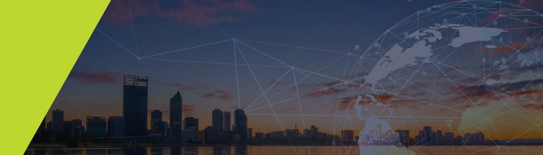
Pursuing climate goals while improving cost efficiency – a decision with impact

The semiconductor industry faces the dual challenge of meeting ambitious climate goals while at the same time operating under significant economic pressure. Fab operators must respond quickly, test new approaches, and evaluate the costs, risks, and time requirements of implementation.


The Software Solution

'Subfab360 ATC' is an innovative software solution developed to increase environmental sustainability in semiconductor production. It enables energy and resource reductions in the subfab which leads to significant reductions in CO2 emissions. Semiconductor manufacturers use the software to control their abatements and pumps in real time based on data from coating and etching systems. 'Subfab360 ATC' is manufacturer-independent and offers simple interfaces for smooth integration of process equipment and subfab devices.

The technological demands in fabs are high – with safety and reliability as top priorities. Algorismic has already completed multiple successful implementations of 'Subfab360 ATC' in Taiwan and Germany, collecting real data on resource savings through case studies. These results can now be experienced interactively in the 'Subfab360 ATC Playroom'.


The Demonstrator: Subfab360 ATC Playroom

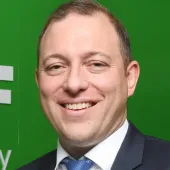
According to Tony Kühn, Director Project Management at algorismic: “The implementation of 'Subfab360 ATC' is no longer an experiment – it is based on real operational experience, has repeatedly proven its effectiveness, and has demonstrated substantial savings potential. This makes it a logical and meaningful solution for any fab aiming to combine efficiency with sustainability.”

In the web application, complex processes are presented interactively and in a way that is easy to understand:

  • The visualization shows a fab: in the cleanroom above, a production tool (e.g., for etching processes); below, in the subfab, the abatement equipment with scrubber and pumps.
  • Without information on gas flows from the production tool and pumps, the abatement equipment runs at full load – with maximum resource consumption.
  • With the software activated, the abatement receives real-time data on gas types and volumes from the production tool and can adjust its energy use for combustion accordingly.
  • In the Savings Reporting, the achieved reductions are clearly displayed and can individually be translated into monetary values.


Highlight Efficiency Potentials

When the significant efficiency potentials in the subfab are made transparent for decision-makers, it provides a much stronger basis for the sustainable decision to implement Active Tool Coupling (ATC). Only by experiencing how the software works together with the achievable resource and cost savings does it become clear how valuable the implementation of 'Subfab360 ATC' is.


Launch at SEMICON Taiwan 2025

At the algorismic gmbh booth at SEMICON Taiwan 2025, German Pavilion, Hall 1, visitors can experience the 'Subfab360 ATC Playroom' interactively and review the underlying case-study data.

Meet us on site: 
TaiNEX 1&2, Taipei, Taiwan
September 10-12, 2025 
at German Pavilion, Hall 1, Booth J2754


About algorismic gmbh

algorismic is an innovative software startup that is committed to an environmentally friendly, low-emission industry. The company develops open-source-based software solutions that help semiconductor manufacturers reduce the environmental impact of production processes and significantly reduce CO2 emissions through sustainable management in subfabs. Whether it‘s significant energy savings or resource consumption, the modular software solutions provide optimization of subfab processes together with useful visualizations. The solutions can be seamlessly integrated into existing IT fab systems and result in lower energy and resource consumption, which contributes to significant cost savings. algorismic was founded in Dresden, Germany in 2023.

Learn more about algorismic on www.algorismic.com


Contact:

Stefanie Hammer, General Manager
linkedin.com/in/stefhammer

algorismic gmbh
Cottaer Str. 4, 01159 Dresden, Saxony, Germany
phone: +49 351 82 44 30
mail: [email protected]
web: www.algorismic.com

Belgium France Germany India Ireland Italy Japan Malaysia Russia Singapore South Korea Taiwan United States Vietnam Webinar_2025-SCM_360x317_Event_Calendar_SCM_2025 Business Executive Technical
Highlighted content

Join us for an insightful webinar as we present the findings from the 2025 Semiconductor Supply Chain Survey, a collaborative effort between the SEMI Supply Chain Management initiative and McKinsey & Company.

The annual survey aims to establish benchmarks for operational agility metrics, covering the entire value chain from material suppliers to OEMs, offering a comprehensive view of the landscape. New this year are additional insights on trends in LTAs and organizational supply chain management capabilities

During this webinar, we will share results from the survey uncovering key trends, challenges, and opportunities within the semiconductor supply chain. By attending, you'll gain valuable insights to benchmark your organization against peers, identify areas for improvement, and course-correct more effectively. Please contact us if you like to learn about how your company can participate in the SCM initiative.

United States

SCM

Join us for a webinar highlighting the 2025 Semiconductor Supply Chain Survey results, conducted by SEMI SCM initiative and McKinsey & Company. Gain fresh insights into operational agility, LTAs, and SCM capabilities across the value chain. Discover key trends, challenges, and opportunities to benchmark your organization and strengthen supply chain resilience.

Choose your session:

9:00 am - 10:00 am Off Add to Calendar 2025-09-23 09:00:00 2025-09-23 10:00:00 2025 Semiconductor Supply Chain survey: Insights for strategy and capabilities Join us for a webinar highlighting the 2025 Semiconductor Supply Chain Survey results, conducted by SEMI SCM initiative and McKinsey & Company. Gain fresh insights into operational agility, LTAs, and SCM capabilities across the value chain. Discover key trends, challenges, and opportunities to benchmark your organization and strengthen supply chain resilience.Choose your session:US/EU: 9:00 AM – 10:00 AM PT [ Register Now ]Asia/US: 5:00 PM – 6:00 PM PT [ Register Now ] United States SEMI.org [email protected] America/Los_Angeles public America/Los_Angeles

Speakers


Henry Marcil

Partner

McKinsey & Company

Bio: Leader in McKinsey’s Advanced Industries Practice, focused on semiconductors n and key end markets (e.g., high tech)

Leads McKinsey’s Resiliency and Geopolitics service line in Semiconductor


Kushal Jolapara

Engagement Manager

McKinsey & Company

Bio: Manager in McKinsey's Operations practice, with a focus on product development and procurement service lines

Leads Supply Chain studies for Advanced Industries clients including Aerospace, Auto and Semiconductors

Dan Peacock

Engagement Manager

McKinsey & Company

Bio: Manager in McKinsey’s Operations Practice, focused on procurement and capital projects

Leads Operations projects at Foundries, IDMs, and equipment clients


Event Contact:

Krish Dharma

[email protected]

Agenda

•    Lead times throughout the semiconductor value chain
•    Landscape and trends in purchasing agreements and LTAs
•    Demand forecasts, backlogs, and end markets
•    Market outlook, opportunities, and threats
•    New for 2025: Organizational capabilities in supply chain management

Event format
Tab Order
Overview
New Tab 2
New Tab 1
Registration
Promote in calendar
Off

Registration for the Global Executive Summit is closed.  Please contact Heidi Hoffman at [email protected] with any questions.  

Belgium France Germany India Ireland Italy Japan Malaysia Russia Singapore South Korea Taiwan United States Vietnam 360x317 GES25 Executive

SEMI Japan has included the Okura Hotel and 3 other hotels convenient to the Okura in the Hotel Block for SEMICON Japan - taking place December 17-19 at Tokyo Big Sight.  View the hotels and rates HERE.

Google Link
Highlighted content

Building on the foundational work of the SEMI Sustainability Climate Consortium and the 2025 Global Climate Summit Workshops (GCSW), this closed-door summit is designed to shift our industry from alignment to action. We are convening a select group of key Executive decision makers & senior leaders from fabs, fabless companies, hyperscalers, and key suppliers and energy partners to: 

  • Showcase and accelerate progress on priority climate initiatives: Abatement, Gas Substitution, Green Materials, and Energy
  • Define clear deliverables and next-phase commitments that unlock scale and momentum
  • Strengthen executive collaboration to remove barriers, share ownership, and drive measurable results

This Summit is not about what we could do — it’s about what we will do, and who will lead.

Click here for the Executive Briefing outlining the event objectives, and the action pathways and methods of engagement for all attendees.  Plan ahead on how presence can shape outcomes that accelerate our industry's decarbonization.

Okura Hotel
Tokyo
Japan

Monday, December 15, 2025

9:00 am - 9:20 am

Coffee & Registration

9:25 am - 9:30 am
 Masahiko (Jim) Hamajima - President, SEMI Japan
Jim Hamajima
President
SEMI Japan

9:30 am - 9:45 am
Ajit Manocha, SEMI
Ajit Manocha
CEO & President
SEMI
Carolin Seward, Google
Carolin Seward
VP of Custom Silicon Sourcing and Operations
Google

GES Opening

9:45 am - 10:25 am
Carolin Seward, Google
Moderator
Carolin Seward
Google
Jinman Han
Jinman Han
President
Samsung Foundry
Jens Liebermann
Jens Liebermann
Senior VP of Global Business
BASF
Sundeep Bajikar
Sundeep Bajikar
Corp. VP Head of Corp Strategy
Applied Materials
Sam Naffziger
Sam Naffziger
SVP & Fellow of Product Technology Architecture
AMD

Fireside Chat: Bending the Curve of Emissions Through Industry Collaboration

Join senior executives from Apple, Samsung Foundry, BASF and Applied Materials, for a discussion on the partnerships required to meaningfully bend the curve towards decarbonization. In an industry already operating under tremendous constraints, what are the lower hanging fruits that are ripe for intentional, precompetitive collaboration? And what can be solved independently?

10:25 am - 10:40 am
Sam Naffziger
Sam Naffziger
SVP & Fellow of Product Technology Architecture
AMD

Spotlight: AMD on the role of Silicon Design for Energy Efficiency

Discover how fabless leaders are driving decarbonization through innovations in energy-efficient product architecture and the critical role of silicon design in minimizing "Use Phase" emissions, the largest contributor to a chip's carbon footprint.

10:40 am - 11:10 am
Anne Meegan
Moderator
Anna Meegan
Director of Sustainability
Google Platforms & Devices
Angela Baker
Angela Baker
VP Sustainability
Qualcomm
Dharmesh Jani
Dharmesh Jani
Director, AI Infra Ecosystem & Partnerships
Meta
Cooper Elsworth
Cooper Elsworth
Sr. TPM, Advanced Energy Labs
Google

End-User Panel: The Decarbonization Imperative

Hear from technology leaders at AMD, Qualcomm, Meta, and Google on why accelerated decarbonization is a business imperative. This panel explores how end-users are (1) acting with a sense of urgency, (2) engaging and enabling their supply chains, (3) driving energy efficient design to drive innovation to accelerate collective progress.

11:10 am - 11:25 am

Break

11:25 am - 11:30 am
Bruce Gall Google
Bruce Gall
Strategic Partnerships
Google

Overview of Priority Initiatives

Priority Initiative: Fab Upstream Materials

11:30 am - 11:40 am
Saifi Usmani, EMD Electronics
Saifi Usmani
VP Global Sustainability
SEMI

Opening Remarks

From Fragmentation to Focus: Outlining a strategy to activate the fab supply chain with a unified customer voice and collaborative support.

11:40 am - 12:10 pm
Bessima
Bessma Aljarbou
Head of Strategy of Environment & Supply Chain Innovation
Apple, Inc.

Keynote: Apple's Supply Chain Engagement

Hear from Apple senior leadership on supply chain engagement and decarbonization, using commercial levers and the power of support and collaboration.

12:10 pm - 12:40 pm
Handy Ko TSMC
Handy Ko
Director, Materials Management
TSMC

From Ambition to Action: A Fab's Role in Upstream Decarbonization

Hear about TSMC's upstream scope 3 (supply chain) decarbonization leadership and recognition of the business imperative, which have been embedded into their core supplier engagement program.

12:40 pm - 12:55 pm
Andrea Jorissen
Andrea Jorissen
Supplier Carbon Solutions
Apple, Inc.

Solutions Enablement & Calls-to-Action

Highlighting clean energy advanced procurement academies and demand aggregation case studies. Announce renewed ambitions and goals for fab upstream scope 3 decarbonization.

12:55 pm - 1:55 pm

Networking & Lunch

Priority Initiative: Clean Electricity

1:55 pm - 2:05 pm
Rebecca Green
Rebecca Green
Partner
ERM
Ken Haig
Ken Haig
Senior Director Government Affairs
Microsoft

Opening Remarks

Setting the stage for collective action on clean electricity in Asia.

2:05 pm - 2:30 pm
Patrick Tan
Patrick Tan
Head of Wider Asia, APAC
Aurora Energy Research

From Visibility to Viability: Developer Insights on Building a Net Zero Future

Hear a market outlook on Clean Electricity in Korea, Japan, and Taiwan, examining current barriers to renewable expansion and the major opportunities driving investment and clean energy growth through 2030.

2:30 pm - 2:55 pm
William Hudson
Will Hudson
Director, Energy & Sustainability Policy
Microsoft

Keynote: Clean Electricity Policy Action & Urgency

Accelerating Clean Electricity expansion requires clear, coordinated policy action. By uniting around shared advocacy priorities, industry and government can remove barriers, unlock renewable supply, and strengthen cost competitiveness across Korea, Japan, and Taiwan.

2:55 pm - 3:25 pm
YS Kim SK HYNIX
Yong Sung Kim
Head of Clean Energy
SK Hynix

Deep Dive: A Clean Semiconductor Partnership in Korea

Explore the proposed Clean Semiconductor Partnership (CSP), SEMI’s flagship initiative to accelerate Clean Electricity development in Korea by aligning industry, government, and utilities on policy reform and procurement innovation, creating a model for collaborative clean energy expansion across Asia.

3:25 pm - 3:40 pm
William Hudson
Will Hudson
Director, Energy & Sustainability Policy, Asia Pacific
Microsoft

Calls to Action

From discussion to action, secure collective advocacy priorities, resource commitments, and endorsement of the Clean Semiconductor Partnership as the pilot for accelerating Clean Electricity expansion across the region.

3:40 pm - 4:10 pm

Break

4:10 pm - 4:50 pm
Rebecca Green
Moderator
Rebecca Green
ERM
Josh Seidenfeld
Josh Seidenfeld
Supply Chain Clean Energy Lead
Google
Chikako Matsumoto
Chikako Matsumoto
Director, Managing Executive Officer
Sumitomo Mitsui Trust Group
Rei Ushikubo
Rei Ushikubo
Director and Head of the Carbon-Free Solutions Division
Shizen Energy
Daisuke Tsujimoto
Daisuke Tsujimoto
Executive Officer, CSO
Renova Inc.

Day 1 Closing Panel: Accelerating Affordability: Scaling Clean Energy Through Collaboration.

How banks, fabs, and retailers can work together to lower renewable energy prices and spread risk, while examining how AI and digital innovation can accelerate price reductions across the supply chain, grid integration, and project development.

4:50 pm - 5:00 pm
Saifi Usmani, EMD Electronics
Saifi Usmani
Vice President, Sustainability
SEMI

Day 1 Closing Remarks and Look Ahead

Reflect on the day's takeaways and action items.

5:00 pm - 6:00 pm

Member-to-Member Meetings / Break

6:00 pm - 6:30 pm

Networking Reception

Join us for Networking in the Orchard Foyer

6:30 pm - 8:30 pm
Alison Drury
Alison Drury
Global Technology Industry Lead
ERM

Dinner with Fireside Chat: “2030 in Focus: Choices That Will Define a Decade”

A forward-looking conversation on how the semiconductor industry can navigate the convergence of climate action, geopolitics, and AI to define its leadership in 2030.

Tuesday, December 16, 2025

8:30 am - 9:15 am

Coffee & Networking

9:15 am - 10:00 am
Saifi Usmani, EMD Electronics
Saifi Usmani
VP Global Sustainability
SEMI

Day 2 Opening

Opening remarks will summarize Day 1 and preview Day 2.

9:30 am - 10:00 am
Lora Ho
Lora Ho
SVP Strategy & ESG
TSMC

TSMC Keynote

Hear from industry leader TSMC on their strategy for decarbonizing advanced semiconductor manufacturing and how it connects to the four GES Priority Initiatives including a new, collaborative path to scale low-GWP gas substitutions from R&D to high-volume manufacturing.

10:00 am - 10:15 am

Break

Priority Initiative: Gas Substitution

10:15 am - 10:25 am
Bruce Gall Google
Bruce Gall
Strategic Partnerships
Google

Opening Remarks

Current efforts to pursue low Global Warming Potential (GWP) gas substitutions in etch and chamber clean applications remain fragmented, resulting in high material costs for HVM application. While promising gas substitutions exist, the traditional paths of small scale or single customer adoption are typically too expensive due to cost scaling limitations. So how do we enable low GWP gas substitutions that also meet cost (as well as performance) expectations? By coordinating a fab-led, industry wide approach to
1) Prioritize a single, low GWP target gas for replacement
2) Co-create and execute a phased experimental plan

10:25 am - 10:45 am
Vahid Vahedi, PhD
Vahid Vahedi
CTO
Lam Research

Equipment Perspective: Scaling Low-GWP Gas Substitution

Hear from a top equipment leader on the process innovations and industry collaboration required to scale low-GWP gas substitution from R&D to high-volume manufacturing

10:45 am - 11:05 am
Steven Scheer
Steve Scheer
SVP Compute System Scaling
imec

imec’s Gas Assessment Platform for Sustainability (GAPS) 

Learn about imec’s Gas Assessment Platform for Sustainability (GAPS) project and how it can be leveraged as an industry test bed for low GWP gas substitution

11:05 am - 11:35 am
Bruce Gall Google
Moderator
Bruce Gall
Google
Rachel Potter EMD
Rachel Potter
VP of Specialty Gas
EMD / Merck
Vahid Vahedi, PhD
Vahid Vahedi
CTO
Lam Research
Steven Scheer
Steve Scheer
SVP Compute System Scaling
imec

It Takes an Ecosystem: A Value Chain Panel on Accelerating Low-GWP Adoption

Hear perspectives from leaders in electronic design automation (EDA), materials, and equipment OEMs on the challenges and opportunities in driving industry adoption of low GWP gases

11:35 am - 11:45 am
Bruce Gall Google
Bruce Gall
Strategic Partnerships
Google

Calls to Action

From Commitment to Action: Outlining the roadmap and action plan for the Gas Substitution Initiative.

11:45 am - 12:45 pm

Networking Lunch

Priority Initiative: Abatement

12:45 pm - 1:10 pm
Beth Elroy
Elizabeth Elroy
VP Sustainability
Micron

Opening Remarks & Keynote

Industry-wide collaboration is critical to accelerate technology innovation and unlock scalable, cost-effective abatement solutions to ease abatement deployment challenges on cost, facilities, space, utilities and operational complexity. Micron will deliver a keynote sharing the abatement journey and the state of current efforts in emission measurement.

1:10 pm - 1:50 pm
Josh Robbins
Moderator
Josh Robbins
Google
Phil Kester
Phil Kester, PhD
Senior Chemical Engineer
Guild Associates
HK KIM KIMM
Dr. Hak-Joon Kim
Korea Institute of Machinery & Materials

F-GHG Catalyst Development & Funding Vehicles

Catalytic abatement remains an important technology, but further research and efforts are needed to identify new catalytic materials, scale performance, and improve their recyclability. Hear from a leading fab and a leading catalyst developer and learn about a promising funding opportunity lead by the Korean government.

1:50 pm - 2:20 pm
Yong Keong Goh
Moderator
Yong Keong Goh
Senior Manager
Micron
Martin Tollner
Martin Tollner
President, Semiconductor Division
Edwards
Morihara Kanken
Atsushi Morihara
Chief Technical Officer
Kanken
Rene Reichardt
Rene Reichardt
CEO
DAS EE
Jong Pil Yoon
Jong Pil Yoon
President
EcoEnergen

F-GHG and Nitrous Oxide Abatement Technology Panel

Abatement technologies are advancing rapidly, and new breakthroughs are on the horizon. Engage with leading abatement suppliers on their outlook on technology roadmaps, strategic priorities and collaborative opportunities.

2:20 pm - 2:30 pm
Kongyeong Goh
YongKeong Goh
Micron
Josh Robbins
Joshua Robbins
Google

Closing Remarks: Abatement

Call-to-actions for commitment to drive high efficiency and low-fuel abatement solutions to accelerate carbon footprint reduction and commercialization, and advance emission measurement technologies to simplify performance verification.

2:30 pm - 2:45 pm
Saifi Usmani, EMD Electronics
Saifi Usmani
VP Global Sustainability
SEMI

Calls to Action Summary & Closing

Hear the takeaways from the Summit and actions for moving forward in our decarbonization journey.

- Sustainability

Semiconductor value-chain executives will gather to align on key initiatives and calls to action, based on our shared decarbonization ambitions, insights and progress thus far.  Together, we will forge an actionable plan for global industry collaboration in three focus areas:  direct emissions, energy-related emissions, and reporting.  This invite-only event will be conducive to accelerating the decarbonization across the industry.

9:00 am - 5:00 pm Off Add to Calendar 2025-12-15 09:00:00 2025-12-16 17:00:00 Global Executive Summit Tokyo 2025 Semiconductor value-chain executives will gather to align on key initiatives and calls to action, based on our shared decarbonization ambitions, insights and progress thus far.  Together, we will forge an actionable plan for global industry collaboration in three focus areas:  direct emissions, energy-related emissions, and reporting.  This invite-only event will be conducive to accelerating the decarbonization across the industry. Okura Hotel Tokyo Japan SEMI.org [email protected] Asia/Tokyo public Asia/Tokyo
Event format
Promote in calendar
Off

Brewer Science Named 2025 National Top Workplace in Manufacturing Industry

Ninth Consecutive Year Receiving 2025 Top Workplace in Greater St. Louis

Rolla, MO – August 7, 2025 – Brewer Science, Inc., a global leader in developing and manufacturing next-generation materials and processes for the microelectronics and optoelectronics industries, has been named a 2025 National Top Workplace in the Manufacturing Industry, marking the fifth consecutive year the company has received this recognition.

Brewer Science has been named 2025 Top Workplaces based on employee feedback

This list is based solely on employee feedback gathered through a third-party survey administered by employee engagement technology partner Energage LLC, a research company with more than 18 years of experience surveying over 27 million employees at 70,000 organizations. Results are calculated by comparing the survey’s research-based statements, including 15 Culture Drivers proven to predict high performance against industry benchmarks.

In addition to being named a National Top Workplace in the Manufacturing Industry, Brewer Science received regional recognition as a 2025 Top Workplace in Greater St. Louis, marking the ninth consecutive year the company has received this recognition.

“Being recognized as a Top Workplace both on a national industry level, as well as locally within our community, speaks volumes to Brewer Science’s dedication in providing our employee-owners with the most fulfilling work experience,” states Dan Brewer, co-CEO at Brewer Science.

Providing customized solutions to customers’ unique, complex situations requires a high regard for a sense of purpose and commitment by everyone within the company. This dedication has been instilled through the company values and creates a workplace flourishing with culture. The employees at Brewer Science are attentive to their roles in the company and the value they articulate to the customers, suppliers, and industry. This has been exemplified by the company becoming Certified Employee-Owned in 2020. Additionally, the company was recognized for meeting the highest corporate social and environmental standards, transparency, and accountability to all stakeholders by becoming a Certified B Corporation™ in 2021.

Learn more about Brewer Science’s company culture and explore career opportunities by visiting our website: https://www.brewerscience.com/about-us/company/careers/

About Brewer Science

Brewer Science is a global leader in developing and manufacturing next-generation materials and processes that foster the technology needed for tomorrow. Since 1981, we’ve expanded our technology portfolio within advanced lithography, advanced packaging, smart devices, and printed electronics to enable cutting-edge microdevices and unique quality monitoring systems for water and air applications. We are Certified Employee-Owned and a Certified B Corporation™, using our business as a force for good. Our headquarters are in Rolla, Missouri, with customer support throughout the world. Learn more at: www.brewerscience.com.

###

Company Contact:

Nathan Ayres

Tel: (US) +1.573.364.0444, ext. 1923

Email: [email protected]

Brewer Science Named 2025 National Top Workplace in Manufacturing Industry

Germany Japan South Korea Taiwan United States ESDA Advocacy Webinar Tile 800x800 Business Technical
Highlighted content

Join us for a webinar that will explore the role of SEMI’s Public Policy and Advocacy (PP&A) team in driving policy developments that are relevant to the ESDA community. PP&A staff will present on SEMI’s advocacy efforts, how you can interface with our team in DC, and how we work with member companies to advance key legislative and advocacy priorities in specific policy areas including:

  • Trade and Export Controls
  • Tax Policy
  • CHIPS Implementation
  • Workforce Development

United States

APHI ESD Alliance SiPAT

The ESD Alliance, a SEMI Technology Community, is hosting a free webinar, "SEMI's Public Policy & Advocacy Office—A Valuable Resource for The Electronic Design Automation Industry," to share how this team can help you navigate global trade complexities and stay ahead of evolving policy challenges. 

10:00 am - 11:00 am Off Add to Calendar Disabled America/Los_Angeles REGISTER NOW
Event format
Promote in calendar
Off

SEMI Members:  $75

Use your corporate email address during log in to be recognized as a SEMI Member.

Non-Members:  $149

Students:  Free

Contact Basak Ulutas Ozturkler ([email protected]) with a picture of your student ID to receive your discount code.

Belgium Germany Singapore Taiwan United States Masterclass #28 Business Executive Technical
Highlighted content

Improved materials are required for progress in fields including printed electronics, semiconductors, aerospace & defense, energy, and life sciences/medical care.  Developing such materials and chemicals involves considerations of performance, cost, manufacturability, safety, and stability.  Scaling production of new materials is a very different challenge than making 50 grams in a laboratory.  Transitioning/commercializing new materials is a separate effort where intellectual property, regulation, quality control, system documentation, supply chain development, and business relationships become key.  This talk will address these aspects of introducing a new material into our enterprise.

ABOUT THE SPEAKER:

Larry Takiff, PhD

Larry Takiff is co-Founder and President of Akita Innovations LLC, a small business in Massachusetts that develops and produces novel chemicals and materials for government and commercial customers.  He founded Akita in 2012 with Lawrence Hancock after working at Polaroid Corporation, Aprilis Inc., and Nomadics/ICx/FLIR Systems.  He is a chemist by training and a businessman by necessity.  At Akita, he has initiated and led projects in materials R&D and pilot production for a variety of government agencies/DoD components and for commercial partners.  Currently he is leading an effort to scale production of a decontamination fluid for the Defense Threat Reduction Agency (DTRA), and a FlexTech project to advance the TRL/MRL of a dielectric ink for printed electronics, as well as several Phase II SBIR development projects.

United States

lt
Larry Takiff, PhD
President
Akita Innovations LLC
Gity Samadi
Moderator
Gity Samadi
Sr. Director, R&D Programs
SEMI
NBMC Smart MedTech FlexTech

Join us for this insightful Master Class with Larry Takiff, PhD, Co-Founder and CEO of Akita Innovations LLC, as he explores the path from lab-scale breakthroughs to scalable material solutions across high-impact industries. Dr. Takiff will dive into the challenges and strategies of transitioning novel materials such as those used in printed electronics, semiconductors, aerospace, and medical devices into commercial success.

10:00 am - 11:30 am Off Add to Calendar 2025-11-12 10:00:00 2025-11-12 11:30:00 FEMC#28 Development, Scaling, and Transition of Novel Chemicals & Materials Join us for this insightful Master Class with Larry Takiff, PhD, Co-Founder and CEO of Akita Innovations LLC, as he explores the path from lab-scale breakthroughs to scalable material solutions across high-impact industries. Dr. Takiff will dive into the challenges and strategies of transitioning novel materials such as those used in printed electronics, semiconductors, aerospace, and medical devices into commercial success. United States SEMI.org [email protected] America/Los_Angeles public Watch on-demand
Event format
Promote in calendar
Off

Lightium, MPI Corporation, and Axiomatic_AI Announce Strategic Partnership to Revolutionize Photonic Integrated Circuit (PIC) Device Testing with AI-Driven Solutions
Zurich, Switzerland; Hsinchu, Taiwan; and Boston, USA – January 6, 2025 – Lightium AG, MPI Corporation, and Axiomatic_AI Inc. have entered into a Memorandum of Understanding (MoU) to jointly develop the world's first Intelligent, Autonomous, and Integrated Test Solution (IAITS) for photonic devices.
This strategic collaboration aims to revolutionize the testing and qualification processes of photonic integrated circuit (PIC) devices by uniting state-of-the-art artificial intelligence, next-generation hardware, and deep domain expertise. The IAITS platform will deliver breakthrough performance in testing workflows—enabling unmatched efficiency, precision, and scalability to meet the ever-evolving demands of the photonics industry.
A Unified Vision for the Future of Photonics Testing
This partnership is driven by a shared commitment to deliver groundbreaking AI driven and self-optimizing solutions to the photonics industry. By combining Axiomatic_AI’s cutting-edge, reasoning-based, self-learning artificial intelligence with MPI Corporation’s industry-leading wafer probing systems and automation software, and leveraging Lightium AG’s advanced testing infrastructure and deep expertise in ultra-high-speed photonic device measurements, the collaboration aims to bring fully integrated, intelligent photonic integrated circuit (PIC) test solutions to market.
Together, the three companies are creating a unified AI platform that addresses the growing complexity and performance demands of characterizing photonic integrated circuits—unlocking new levels of automation, precision, and scalability for next-generation applications.
Disruptive Value Creation Across Hardware and Human Resources
The Intelligent, Autonomous, and Integrated Test Solution (IAITS) introduces a new paradigm in photonic integrated circuit (PIC) testing, delivering transformative value across both technology infrastructure and human capital.
Key Benefits of IAITS:
• Increased Throughput: By automating complex test routines, minimizing downtime, and optimizing measurement system utilization, IAITS significantly accelerates test cycles and reduces iteration times.
• Enhanced Human Efficiency: The system reduces reliance on manual operation, programming, and debugging—freeing skilled personnel to focus on high-value engineering and strategic innovation tasks.
IAITS will be commercially available as an advanced software add-on package for MPI Corporation’s wafer probing systems. Designed to support both R&D and high-volume production environments, the solution sets a new industry benchmark for efficiency, precision, and scalability—ultimately lowering the total cost of testing and accelerating time-to-market for next-generation PIC devices.
About Lightium AG
Lightium AG is a Swiss-based startup specializing in Photonic Integrated Circuit (PIC) foundry and design services, built on its proprietary, production-grade Thin-Film Lithium Niobate (TFLN) platform. Lightium accelerates customer innovation by delivering unmatched photonic performance, a streamlined and cost-efficient supply chain, and seamless scalability from prototyping to high-volume manufacturing.
As Europe’s first production-grade TFLN foundry, Lightium plays a pivotal role in enabling next-generation photonic solutions across a diverse range of industries, including telecommunications, data communications, quantum computing, artificial intelligence, and space technologies.
Further information can be found at: Lightium - Thin Film Lithium Niobate (TFLN) Photonic Foundry
About MPI Corporation
MPI Corporation, headquartered in Taiwan, is a global leader in advanced probe systems and testing solutions for the semiconductor, photonic, and photonic integrated circuit (PIC) industries. The company designs and manufactures high-performance wafer probing systems known for their exceptional precision, automation capabilities, and scalability—empowering cutting-edge testing across research, development, and high-volume production.
MPI’s innovations play a critical role in advancing next-generation technologies in wireless communication, electronics, and photonics. The company is publicly listed on the Taipei Exchange (TAIEX: 6223).
For more information, please visit: About MPI Corporation – Global Semiconductor Testing Leader
About Axiomatic_AI Inc.
Axiomatic_AI Inc., headquartered in Boston, is a pioneering startup developing physics-based reasoning artificial intelligence to accelerate innovation and reduce the cost and risk associated with deep-tech development. Its cutting-edge AI technologies are redefining how high-tech industries design, measure, and optimize complex systems—enabling faster, smarter decision-making across R&D and production environments.
Axiomatic_AI’s mission is to unlock new efficiencies and capabilities in fields where precision and complexity are paramount.
Learn more at: https://axiomatic-ai.com/mission/

Kitchener, Ontario, July 15, 2025 – PEER Group®, the largest supplier of innovative factory automation software products for the semiconductor industry has launched a new service offering to help OEMs comply with the SEMI® Cybersecurity Standard E187: Specification for Cybersecurity of Fab Equipment.

“PEER Group’s new PEER® E187 Compliance Assessment is a comprehensive third-party service for OEMs that provides the essential training, assessment, documentation, and guidance to help their equipment comply with SEMI E187,” says Doug Suerich, PEER Group’s Director of Marketing.

Released in 2022, SEMI E187 provides a baseline level of security for new equipment being shipped to factories. It applies specifically to computing devices installed on fab equipment that run Microsoft Windows or Linux. Already mandatory at some factories, SEMI E187 is being increasingly adopted as part of factory acceptance requirements.

“PEER Group is uniquely positioned to assist with E187 compliance thanks our leadership in SEMI’s Semiconductor Manufacturing Cybersecurity Consortium (SMCC), participation in SEMI Standards development, and our decades of experience working with both OEMs and factories to meet fab specification requirements and achieve SEMI Standards compliance,” shares Suerich, who also serves as an SMCC Governing Council member.

To help educate OEMs on how to comply with SEMI E187, PEER Group is hosting a free webinar on July 24, 2025. For more information, including how to register, visit: https://attendee.gotowebinar.com/register/7410295402908186710?source=se…

About PEER Group
PEER Group® is the leading global supplier of innovative factory and tool automation and connectivity software for the semiconductor industry. Since our founding in 1992, we have been committed to developing best-in-class solutions that help OEMs and factories reduce their time to market, risk, and costs by solving their most challenging automation, connectivity, and SEMI Standards compliance problems. Follow PEER Group on. Follow PEER Group on LinkedIn.

This cutting-edge panel-level wet processing demo tool handles large 510 × 515 mm substrates, delivering world class, high density Through Glass Vias (TGV) formation and ultra-small taper angles essential for advanced packaging in high performance computing.

Gütenbach, Germany – July 15, 2025 – RENA Technologies, a leading manufacturer of wet processing equipment for semiconductor and advanced packaging production, today announced the ramp-up of its dedicated glass core substrates facility in Germany. This new line, designed for substrates up to 510 × 515 mm, immediately opens for customer test lots, underscoring RENA's proven expertise in glass processing and creating new opportunities for process development and customer sample production. “As experts in precision wet processing, we can now offer large panel demo services for high aspect ratio through glass via (TGV) formation on various glass types,” said Dr. Holger H. Kuehnlein, SVP Technology at RENA. “Our alkaline based TGV process delivers extremely small taper angles, low sidewall roughness, and exceptional dimensional control at panel scale, enabling high density via applications. Customers can begin validating these capabilities today.”

Why Glass, and Why Wet Processing?
Glass substrates offer significant advantages for advanced electronics, including ultra-flat surfaces, low dielectric loss, and superior thermal stability. However, realizing these benefits at scale requires defect free surface preparation and the formation of uniform, high density TGVs with minimal taper angles. RENA's wet processing systems are specifically designed to address both challenges:
1. Surface Engineering – Our systems ensure precise cleaning and stress relief across 600 x 600mm panels with submicron total thickness variation (TTV).
2. Chemically Formed TGVs – Following initial laser modifications performed by our specialist partners, RENA’s proprietary chemistries form, enlarge and shape each via to exact specifications. This process consistently delivers very small taper angles and smooth sidewalls, ideal for subsequent metallization.

By collaborating with leading German and international laser partners, RENA offers customers the flexibility to choose their preferred laser vendor while ensuring all downstream wet processing steps are handled by our advanced equipment.

Key Highlights of the New Facility
Panel Size: Focus on 510 x 515mm and up to 600 × 600mm, smaller possible
Tool Set: Alkaline TGV etching, advanced rinse/dry, optical inspection & metrology
Field-Proven Recipes: Process conditions migrated from high volume tools
On-Demand Access: Customers may run demo substrates, qualify custom chemistries, or request full process flows
Sustainability: Low temperature chemistries and closed loop water reclamation reduce energy and ultrapure water (UPW) consumption

Market Impact
High-Performance Computing (HPC) as well as 5G/6G RF modules increasingly require new package designs, including panel-level fan-out and trend towards more complex chiplet architectures. Glass substrates, long considered the “holy grail” for core and interposer material, effectively eliminate the limitations imposed by warpage and dielectric loss in organic substrates. By combining laser modification from our vetted partners with RENA's chemistry driven via shaping, designers can now validate glass packaging concepts on the lab-platform proven at 600x600mm dimensions.
“With this lab-tool, we've created a great opportunity for semiconductor manufacturers to perform demos on panel level glass substrates,” added Peter Schneidewind, CEO of RENA. “From surface preparation to via formation, our wet process flow is ready for customers substrates to support TGV technology breakthroughs. This is world class made in Black Forest.”

Availability & Engagement Model
• Testing available now
• Flexible collaboration: Bring your own laser modified substrates, or leverage RENA’s ecosystem partners to benefit from joint process development support, and metrology services for process validation.

About RENA Technologies GmbH
RENA Technologies is a leading global supplier of production machines for wet chemical surface preparation. RENA products are used in path-breaking application fields such as semiconductors, MedTech, renewable energies, the glass industry and additive manufacturing. RENA equipment is used to treat or modify surfaces of, for example, semiconductor wafers, solar cells, glass, optical substrates, 3D-printed metal components or other high-tech products using wet chemical processes. RENA offers proven standard machines as well as customer-specific solutions and process support.

CONTACT
Sales:
Felix Fink
Phone: +49 7723 9313-403
E-Mail: [email protected]

Press:
Dirk Hensel
Phone:+49 7723 9313-914
E-Mail: [email protected]
www.rena.com