Meet your branding and marketing objectives with a customized sponsorship package. Become a sponsor and brand your company to an influential audience of executives at ESDA/CEDA Phil Kaufman Awards.
Contact Tim Janes, [email protected], +1.720.939.4992 to learn more.
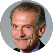
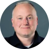
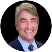
Electronic System Design Alliance—ESDA and IEEE Council on EDA—CEDA are proud to honor
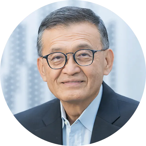
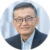
LIP-BU TAN
CEO, Intel and Former CEO, Cadence Design Systems with the
2025 Phil Kaufman Award
2025 Award Recipient
Lip-Bu Tan is receiving this honor for his leadership and business impact on the Electronic Design Automation industry, a critical part of the global semiconductor supply chain.
Lip-Bu Tan’s influence shaped the direction of the semiconductor industry through his visionary leadership and strategic initiatives. Lip-Bu has an exceptional ability to spot important technology trends years before others see them. His ability to set a clear technical direction and inspire teams has had a lasting impact on the broader technology landscape.
Lip-Bu Tan will be honored at the 2025 Phil Kaufman Award Ceremony and Banquet on November 6, 2025 in San Jose, CA.
The Phil Kaufman Award honors individuals who have had a demonstrable impact on the field of electronic system design through technology innovations, education/mentoring, or business or industry leadership. The award was established as a tribute to Phil Kaufman, the late industry pioneer who turned innovative technologies into commercial businesses that have benefited electronic designers.
Phil Kaufman Award & Banquet
6:30 pm - 9:00 pm
Off
Add to Calendar Disabled
America/Los_Angeles
1
Registration covers all 3 days of Workshops. No discounts given for partial attendance. Full refunds through December 17, 2022. December 18-January 19 - substitutions only.
SEMI, FlexTech, NBMC & NextFlex Members: $199
Non-Members: $499
If you have any questions, please contact Gity Samadi, [email protected].
Step 2 – Choose Rate Preference, then group rate, type in SJ1
Alternatively, you may email the General Manager at [email protected]
HEALTH AND SAFETY
Your health and safety are our top priority. We monitor developing federal, state, and local health and safety recommendations and requirements to determine the most appropriate safety protocols for our in-person events. For international attendees arriving from outside of the United States, please review the government travel guidance to confirm eligibility and requirements for travel.
FACE COVERINGS
Although masks are not required, attendees are encouraged to determine use based on their own personal comfort level as well as to be respectful of other's individual choice.
Highlighted content
SEMI FlexTech FHE Technical Gap Analysis Workshop - Tues. 1/17 - 8 am-12 noon
@ SEMI - 673 S. Milpitas Blvd - Milpitas, CA
During this workshop the attendees will complete a Technical Gap Analysis in preparation for FlexTech’s next Request for Proposals (RFP), including exploring topics and technology development required to meet development objectives. Lunch will be served following the workshop.
SEMI NBMC Technical Gap Analysis Workshop - Tues. 1/17 - 1:00-5:00 pm
@ SEMI - 673 S. Milpitas Blvd - Milpitas, CA
Attendees will turn their sights to preparing the technical topics / gaps in the Nano-Bio Materials space to explore topics and technology development required to meet development objectives. A networking reception will follow the workshop.
Many topics and paths were identified at the previous, very successful workshop in July 2022. This workshop will take the work a step further and create scopes of work for this very important foundation required to propel the design in of FHE-based components. This workshop includes a continental breakfast and lunch.
NextFlex - Hybrid Electronics for Advanced Packaging Workshop - Wed 1/18 2:00 - 7:00 pm & Thurs 1/19 - 8:00 am - 5:00 pm
@NextFlex, 2244 Blach Place, Suite 150, San Jose, CA
As the community awaits the release of request for proposals (RFPs) for programs within the CHIPS and Science Act, NextFlex is hosting a workshop to align the ecosystem’s vision on how additive hybrid electronics manufacturing can shape the future of domestic advanced semiconductor packaging. Join us for presentations from visionary speakers on how their organizations plan to participate in the CHIPS and Science Act programs and participate in breakout sessions focused on information sharing, proposal concept refinement, and formation of proposal teams.
Breakout topics include:
Direct Write Interconnects
Substrates and Buildup Layers
Interposers, Bridges & Architectures
Circuitization
SEMI & NEXTFLEX Milpitas & San Jose, CA United States
Tuesday, January 17 @ SEMI Milpitas
8:00 am
-
8:30 am
Continental Breakfast
SEMI FlexTech FHE Technical Gap Analysis Workshop
8:30 am
-
8:45 am
Melissa Grupen-Shemansky
CTO & VP, Technology Communities
SEMI
Introduction
8:45 am
-
9:00 am
Eric Forsythe, PhD
Program Manager
ARL
RFP Process and Background
9:00 am
-
9:15 am
Robert Praino
Chief Innovation Officer & Co-Founder
CHASM Advanced Materials
A Look Back and The Path Ahead & RFP Process
9:15 am
-
10:45 am
Breakout Sessions for Technical Gap Analysis
10:45 am
-
11:00 am
Break
11:00 am
-
11:45 am
Break out Review & Summary
11:45 am
Wrap-Up
12:00 pm
-
1:00 pm
Lunch
NBMC Technical Gap Analysis Workshop
1:00 pm
-
1:15 pm
Melissa Grupen-Shemansky
CTO & VP, Technology Communities
SEMI
Introduction
1:15 pm
-
1:30 pm
Gina Tollefson
Program Manager
AFRL
NBMC 2023
1:30 pm
-
1:45 pm
Azar Alizadeh
Principal Scientist
GE Research
RFP Process & Insights
1:45 pm
-
2:00 pm
Break
2:00 pm
-
4:00 pm
NBMC Break Out Sessions
4:00 pm
-
4:45 pm
Final Review & Summary
4:45 pm
-
5:00 pm
Wrap-Up
5:00 pm
-
7:00 pm
Reception & Networking
Wednesday, January 18, 2022
FHE Standards Workshop
8:00 am
-
8:30 am
Continental Breakfast
8:30 am
-
8:45 am
Gity Samadi
Sr. Director of R&D Programs
SEMI
Paul Trio
Director, SEMI Standards
SEMI
Introduction of Project & Status
8:45 am
-
9:15 am
Randall Parker
American Semiconductor
The Need for Standards in Flexible & Printed Electronics
9:15 am
-
10:45 am
Breakout Session on Selected Topics
10:45 am
-
11:00 am
Break
11:00 am
-
11:45 am
Review and Summaries from Breakouts
11:45 am
-
12:00 pm
Wrap-Up
12:00 pm
-
1:00 pm
Lunch
1:00 pm
-
2:00 pm
Travel Time to NextFlex -
For a detailed program agenda for this workshop visit NextFlex.us
Join us for three-days of technology assessments, updates, discovery and planning workshops focused on the development of the electronics ecosystem and flexible, hybrid electronics, medical monitoring sensors, and their application to driving development in new electronics packaging approaches.
Industry experts and leaders will come together to focus on identifying gaps in technology development, including in design, manufacturing, standards and environmental sustainability.
The Evolution of Electronics
2023 Technology Workshops:
- NBMC Gap Analysis
- FHE Gap Analysis
- FHE Standards
- Hybrid Electronics for Advanced Packaging
8:00 am - 5:00 pm
Off
Add to Calendar Disabled
America/Los_Angeles
How to Protect Your Invention
Registration
SEMI Members: $49
Use your corporate email address during log in to be recognized as a SEMI Member.
Non-Members: $99
Students: Free
Contact Gity Samadi ([email protected]) with a picture of your student ID to receive your discount code.
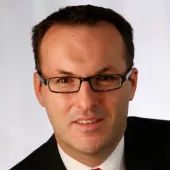
Harvey Kauget practices in the firm's Corporate Practice Group with a focus on intellectual property litigation and prosecution.
Harvey serves a wide-range of clients in the areas of patent, trademark and trade secret litigation, patent and trademark prosecution, IP risk management, portfolio licensing, and client counseling.
Harvey’s litigation and patent prosecution background consists of dealing with matters related to technologies such as: semiconductor processing, plasma dicing, welding systems, lighting and LEDs, hot plates, software, computer integration and networking, satellites, solar power, hydrogen fuel cells, biodiesel, gaming, jewelry, gift cards, cups, davit lift, suntan lotions, power tools, paint rollers, flow systems, nuclear control rods, shirt pressers, air filters, hot water systems, fans, contact lenses, blood plasma expander, disposable blood measuring device, urine analysis, teeth whitening, suture anchors, and medical devices. In addition, he also has experience in a wide-range of other areas including firearms, speakers, waste fuel flare stacks, furniture, exercise equipment, recycling equipment, cement materials, fence posts, and tidal gates.
Mr. Kauget has experience presenting cases before the Court of Appeals for the Federal Circuit and Eleventh Circuit. He is also a registered patent attorney admitted to practice before the U.S. Patent and Trademark office. Before Harvey began his legal career, he worked as an engineer and as a product manager in the semiconductor industry as well as a certified high school chemistry and physics teacher.
Honors & Recognitions
Listed in The Best Lawyers in America®️, "Lawyer of the Year," Trademark Law, Tampa, Florida (2022 & 2023)
Listed in The Best Lawyers in America®️, Information Technology Law since 2008, Litigation - Intellectual Property since 2011, Litigation - Patent since 2011, Patent Law since 2011, Technology Law since 2010, Trademark Law since 2011, Trade Secrets Law since 2021
Named, Chambers USA, Intellectual Property (2021-2022)
Listed in The Best Lawyers in America®️, "Lawyer of the Year," Patent Law, Tampa, Florida (2015, 2018, 2019, & 2021)
Receive practical information on designing, writing and protecting your patents from an experienced and knowledgeable source. This course will review the latest thinking in what is a patentable invention and how to protect your invention. You will learn the basics of disclosing your invention for maximizing your protection, with an opportunity for Q&A at the end. A course useful to inventors at every stage of your careers and every stop in our industry ecosystem.
How to Protect your patent
Flexible Electronics Master Class #14
10:00 am - 12:00 pm
Off
Add to Calendar Disabled
America/Los_Angeles
Flexible hybrid electronics (FHE) is an emerging manufacturing methodology that combines the best of conventional and printed circuitry. By enabling flexibility and digital manufacturing without compromising on processing capability, it promises to remove the constraints of rigid PCBs while reducing costs and hence enable new applications.
This webinar from Dr Matthew Dyson of IDTechEx provided the status of FHE, including examples that are already commercialized.
Standards and other attributes required for mass manufacturing was outlined, and the scope for FHE to be used for novel applications (including harsh environments) assessed. Finally, a roadmap covering the near, medium, and long term was presented, including how FHE development fits with the ongoing development of heterogeneous integration.
ABOUT THE SPEAKER
Matthew is a Senior Technology Analyst at IDTechEx, specializing in printed/organic/flexible/hybrid electronics and sensors. He has an MRes and PhD in Physics from Imperial College London, which aimed to better establish processing/structure/property relationships in organic semiconductors. This was followed by two years post-doctoral researcher at Eindhoven Technical University in the Netherlands, focusing primarily on organic photodetectors (OPDs). His academic research, which has been cited over 500 times, also included work on perovskite photovoltaics and aggregation induced emission materials.
At IDTechEx, Matthew analyses technical innovations and applications across the printed/flexible/hybrid landscape, attending multiple conferences and interviewing companies to establish a clear picture of the technical and commercial landscape. This analysis is published in reports on topics such as 3D electronics and printed/flexible sensors, and applied to consulting projects evaluating commercialization opportunities across printed/flexible electronics. He also manages a team of analysts covering wearable technologies, AR/VR, and emerging photovoltaics.
United States
Dr. Craig Milroy
National Research Council (NRC) Research Associate
This webinar featured Dr. Matthew Dyson of IDTechEx outlining the status of FHE, including examples that are already commercialized. Standards and other attributes required for mass manufacturing were discussed, and the scope for FHE to be used for novel applications (including harsh environments) assessed. In addition, he presented a roadmap covering the near, medium, and long term will be presented, including how FHE development fits with the ongoing development of heterogeneous integration.
FHE Market Forecast & Review
Flexible Electronics Master Class #13
8:00 am - 9:00 am
Off
Add to Calendar Disabled
America/Los_Angeles
-
Off
Add to Calendar2022-11-17 00:00:002022-11-18 00:00:002022 SEMI China Semiconductor Supply Chain International Forum (SEMI China Member Day)Shenzhen ChinaSEMI.org[email protected]America/Los_Angelespublic
-
Off
Add to Calendar2022-11-17 00:00:002022-11-18 00:00:002022 SEMI中国半导体供应链国际论坛暨SEMI中国会员日Shenzhen ChinaSEMI.org[email protected]America/Los_Angelespublic
[Northeast Forum 2022] Future Infrastructure—The Impact on the Semiconductor Industry
FUTURE INFRASTRUCTURE—The Impact on the Semiconductor Industry
The SEMI Northeast Forum will bring together industry leaders from the semiconductor supply chain to discuss their vision of the impact of new technologies and applications on the semiconductor industry.
Although we often hear about the end of Moore’s law, expanding markets such as 5G, autonomous vehicles, AI, medical technologies, and improving the energy infrastructure have provided new challenges that foster new innovations. Technologies such as heterogenous integration allowed the industry to migrate from chip scaling to system scaling to address these new applications. These new technologies and applications bring new challenges to the entire ecosystem.
Hear Linx Consulting, Breker, and Teledyne give their insight on:
Heterogeneous Integration
Supply Chain Impact
Verification and Packaging Challenges
Join your colleagues on October 27 to hear industry experts outline a new playbook for innovation that can propel the industry into the next wave of growth.
Teradyne 600 Riverpark Drive North Reading, MA01864 United States
THURSDAY, OCTOBER 27, 2022 | EASTERN TIME
10:00 am
-
10:05 am
Northeast Regional Chair
Mark Kahwati
Senior Director of Product Marketing
Teradyne
Welcome
10:05 am
-
10:35 am
Mark Thirsk
Managing Partner
Linx Consulting
Supply Chain Impact
10:35 am
-
11:05 am
Dave Kelf
Chief Executive Officer
Breker Verification Systems
Changing Product Requirements
11:05 am
-
11:35 am
Eric Shoemaker
Director of Marketing, Test Interface Solutions
Teradyne
Future Testing Challenges
11:35 am
-
12:05 pm
Christy Tyberg
Sr. Manager, Quantum Hardware Technology Development
IBM
Quantum Computing
12:05 pm
-
12:45 pm
Lunch
12:45 pm
Closing Remarks
The SEMI Northeast Chapter Presents—
Future Infrastructure—The Impact on the Semiconductor Industry
SEMI Northeast Forum
In-Person
October 27, 2022 10:00am–1:00pm ET
10:00 am - 1:00 pm
Off
Add to Calendar2022-10-27 10:00:002022-10-27 13:00:00[Northeast Forum 2022] Future Infrastructure—The Impact on the Semiconductor IndustryThe SEMI Northeast Chapter Presents—Teradyne 600 Riverpark Drive North Reading, MA 01864 United StatesSEMI.org[email protected]America/New_Yorkpublic
America/New_York
Semiconductor technology advancements and added device complexity put ever more stringent requirements on semiconductor manufacturing process monitor and control. Pressure exerted on devices during grinding, CMP, polishing, lamination, bonding, pick and place encapsulation, electrical testing, and packaging can cause failures that may not even be measurable using conventional sensors.
Currently chip test, monitoring and packaging process control is widely done via optical displacement sensors and electrical testing which do not adequately measure the pressure on devices. Without the ability to adequately monitor these processes, root cause failure identification is challenging and maintaining or improving process quality and yield are difficult.
In this webinar the piezoelectric sensor technology will be described and how it used to improve chip test, monitoring and packaging semiconductor processes.
Learn how high-sensitivity, high dynamic range piezo dynamic force measurement sensors can be used to better measure strain during grinding, CMP, polishing, lamination, and electrical test.
MSIG Webinar: Ultra-sensitive, high bandwidth piezoelectric pressure sensors
First in the Innovative Sensors Webinar Series
8:00 am - 9:00 am
Off
Add to Calendar Disabled
America/Los_Angeles