downloadGroupGroupnoun_press release_995423_000000 copyGroupnoun_Feed_96767_000000Group 19noun_pictures_1817522_000000Member company iconResource item iconStore item iconGroup 19Group 19noun_Photo_2085192_000000 Copynoun_presentation_2096081_000000Group 19Group Copy 7noun_webinar_692730_000000Path
Skip to main content
Default Banner Image

South Korea

South Korea Standards main.jpg

SEMI Korea Office
Seoul
South Korea

Standards

Information & Control Korea TC Chapter 

Date: Friday, November 27, 2020

Time: 15:00-17:00 (KST)

Via Hybrid


AGENDA

(Subject to change)

Last updated: October 26, 2020


NOTE:

Standards meetings are open to all, but you must be a SEMI Standards Program Member to attend. If you are not a Member, please join the Standards Program and start making a big contribution to the industry’s progress, complete an application form today!
Questions? Contact your local staff coordinator: Click here

3:00 pm - 5:00 pm Off Add to Calendar 2020-11-27 15:00:00 2020-11-27 17:00:00 I&C Korea TC Chapter Meeting Information & Control Korea TC Chapter  Date: Friday, November 27, 2020 Time: 15:00-17:00 (KST) Via Hybrid   AGENDA (Subject to change) Last updated: October 26, 2020   NOTE: Standards meetings are open to all, but you must be a SEMI Standards Program Member to attend. If you are not a Member, please join the Standards Program and start making a big contribution to the industry’s progress, complete an application form today! Questions? Contact your local staff coordinator: Click here SEMI Korea Office Seoul South Korea SEMI.org [email protected] Asia/Seoul public Asia/Seoul

At IMAPS 2020 MRSI Systems will introduce a new 5 micrometer die bonder product, MRSI-705 high-volume configuration. The MRSI-705 was first introduced in 2012 and has enjoyed a dominant position in the die bonding industry offering customers multiple application solutions in one machine. This new configuration offers an innovative horizontal turret feature to significantly increase the speed and throughput from the machine without sacrificing its renowned flexibility, accuracy, or reliability.

The new MRSI proprietary design delivers an “on-the-fly” tool change with up to 12 tools with zero tool changeover downtime, which has been an integral part of MRSI’s popular high-speed product lines MRSI-HVM and MRSI-H. This leads to increased machine efficiency, higher production output, and lower manufacturing costs.

This flexible 5 micrometer die bonder retains its comprehensive appeal across a wide range of applications including photonic packaging, microwave modules, RF power amplifiers, and infrared sensors.

“The addition of this new high-speed 5 micrometer die bonder re-enforces MRSI’s industry-leading position in the field of manufacturing automation for advanced microelectronic and optoelectronic devices. We look forward to working with customers to help them to scale their production,” said Dr. Yi Qian, VP & GM MRSI Systems, Mycronic.

To schedule an appointment and discuss a prototype demonstration, please contact us at [email protected].

For additional information, please contact:
Dr. Limin Zhou
Senior Director, Strategic Marketing, MRSI Systems
Tel: +86 135 0289 9401, e-mail: [email protected]
Time Zone: CST – China Standard Time

About MRSI Systems
MRSI Systems, part of Mycronic Group, is the leading manufacturer of fully automated, high-speed, high-precision and flexible eutectic and epoxy die bonding systems. We offer “one-stop-shop” solutions for research and development, low-to-medium volume production, and high- volume manufacturing of photonic devices such as lasers, detectors, modulators, AOCs, WDM/EML TO-Cans, Optical transceivers, LiDAR, VR/AR, sensors, and optical imaging products. With 30+ years of industry experience and our worldwide local technical support team, we provide the most effective systems and assembly solutions for all packaging levels including chip-on-wafer (CoW), chip-on-carrier (CoC), PCB, and gold-box packaging. www.mrsisystems.com

About Mycronic
Mycronic AB is a Swedish high-tech company engaged in the development, manufacture and marketing of production equipment with high precision and flexibility requirements for the electronics industry. Mycronic headquarters are located in Täby, north of Stockholm and the Group has subsidiaries in China, France, Germany, Japan, Singapore, South Korea, the Netherlands, United Kingdom and the United States. Mycronic AB (publ) is listed on NASDAQ Stockholm. www.mycronic.com

Facebook Twitter Pinterest LinkedInShare

Santa Clara – Sept. 29, 2020 – Picarro Inc., a leading provider of trace gas analyzers for a variety of air monitoring applications, is expanding its presence in Asia by opening a customer service and support office in Hwaseong, South Korea. Having sales staff, repair services, and replacement parts available locally will allow the company to better support its growing customer base there.

“Our portfolio of extremely sensitive and accurate analyzers enables semiconductor and equipment manufacturers to identify and mitigate airborne molecular contamination in the fab faster, resulting in better yield,” said John Park, General Manager at Picarro. “With several key semiconductor fabs and equipment manufacturers located in South Korea, and increasing adoption of our scientific instruments in other industries, it’s important that we have a robust presence there.”

John Park will head up the Korea office. Park has more than 20 years of experience in the semiconductor equipment and materials business in Korea. Prior to joining Picarro, he led successful sales teams at Tosoh SMD Korea and UnitTest Inc. and has established relationships with leading electronics and semiconductor companies there. He earned a B.A. in metallurgical engineering at Ulsan University in Korea.

About Picarro
Picarro provides industry leading solutions for real-time AMC monitoring. Their cavity ring-down spectroscopy (CRDS) technology offers significant advantages compared with incumbent AMC measurement techniques, such as ion-mobility spectrometry (IMS) and ion chromatography. Picarro’s SI Series analyzers enable fast response to contaminants in the cleanroom in seconds, not hours. With real-time continuous parts-per-trillion (ppt) level analysis, Picarro analyzers provide early warning of contamination events for AMC monitoring in cleanrooms, FOUP, and fab equipment.

For additional information, please visit semi.picarro.com

###

Contact:
Siiri Hage
Director of Marketing Communications
Picarro, Inc.
[email protected]

ESPOO, Finland, 24th September 2020 – Picosun Group, the leading supplier of AGILE ALD® (Atomic Layer Deposition) thin film coating technology, reports excellent results in UVC (ultraviolet-C) LED performance, achieved with the company’s ALD solutions.

Excellent reliability and lifetime improvements of UVC LEDs have been obtained at Picosun’s customer and collaboration partner site, National Chiao Tung University (NCTU), Taiwan, using passivation and barrier films deposited with PICOSUN® ALD equipment(*). ALD passivation layer could potentially replace the expensive hermetic seal package of the LEDs and thus lower the costs of the final device.

“We have used Picosun’s ALD technology already for years with great success. Our PICOSUN® ALD equipment yields superior quality films which has helped us to achieve several breakthroughs in our LED research. Picosun has local presence in Taiwan and we appreciate the prompt response of their customer support if we ever have any issues. At the phase when R&D results are to be ramped up to industrial-level production, the scalability of Picosun’s ALD technology is a huge benefit,” comments Professor Hao-Chung Kuo from NCTU.

In order to reach maximum light output and long operating lifetime, LED chips require surface passivation to eliminate parasitic currents caused by traps and defects. Also barrier coating is typically needed as LED materials are sensitive to moisture. ALD is an ideal technique to manufacture both the passivation and barrier films – and when the LED size diminishes to micrometer dimensions, the only coating method capable of producing high enough quality films on the required minuscule scale. Ultra-thin, pinhole-free ALD films do not suppress the LED light intensity and they provide reliable protection against ambient conditions, whereas their superior conformality ensures no thickness variations between the facets of the LED chip. Thickness variations, typical side effect of other coating methods, can potentially lead to uneven distribution of film stress or thermal expansion behavior and risk physical damage of the chip.

Short-wavelength UVC radiation destroys bacteria and viruses so UVC LED technology is particularly topical now during the still ongoing COVID-19 pandemic. Small, lightweight LEDs enable versatile design of portable, compact disinfecting equipment, they consume less power than other UVC sources, they are durable, and they pose no risk of hazardous material leaks such as e.g. mercury lamps.

“We are happy of the achievements of Professor Kuo’s group at NCTU, and how Picosun’s ALD technology has helped them to achieve their goals in UVC LED development. Our long-term collaboration and networking with both the academia and prominent industries in this field gives us the perfect synergy advantage to facilitate implementation of these solutions in industrial manufacturing,” says Mr. Edwin Wu, CEO of Picosun Asia Pte. Ltd.

(*) UVC LED with 50 nm ALD Al2O3 passivation and normal LED packaging (no hermetic seal) maintained 80% of its original efficiency even after 500 hours environmental test at 85% humidity and 85 oC temperature.

About Picosun
Picosun provides the most advanced AGILE ALD® (Atomic Layer Deposition) thin film coating solutions for global industries. Picosun’s ALD solutions enable technological leap into the future, with turn-key production processes and unmatched, pioneering expertise in the field – dating back to the invention of the technology itself. Today, PICOSUN® ALD equipment are in daily manufacturing use in numerous leading industries around the world. Picosun is based in Finland, with subsidiaries in Germany, USA, Singapore, Taiwan, China, Korea and Japan, offices in India and France, and a world-wide sales and support network. Visit www.picosun.com.

More information:
Mr. Edwin Wu
CEO, Picosun Asia Pte. Ltd.
Tel: +358 40 480 3449
Email: [email protected]
Web: www.picosun.com

Kalispell, MT – Semiconductor equipment manufacturer ClassOne Technology announced the sale of its Solstice® LT electroplating system to Jenoptik for manufacturing semiconductor material for high-power diode lasers at its semiconductor production facility in Berlin-Adlershof, Germany. High-power diode lasers play an important role in optical pumping of solid-state lasers as well as in direct use applications such as material processing, sensing as well as in healthcare & life science. The dual-chambered Solstice LT is specially configured for high-performance gold processing. The announcement was made jointly by ClassOne CEO, Byron Exarcos, and Dr. Juergen Sebastian, plant manager of the Jenoptik facility in Berlin.

"The new Solstice LT will replace a manual plating wet bench," explained Dr. Sebastian. “This will significantly improve process stability, plating quality as well as reduce our metallization step costs. That’s important because at Jenoptik, we build all the semiconductors that go into our diode lasers in-house. The new Solstice LT electroplating system thus ensures very high quality, performance and service life of our end products. Moreover, the new system also promotes Jenoptik’s policy of sustainability thanks to the new electrolyte technology.”

“The Solstice LT for Jenoptik is specially configured with our GoldPro™ processing chamber,” said Exarcos. “GoldPro can deliver unprecedented levels of repeatability – wafer-to-wafer, die-to-die, within-die, and within-feature. The bottom line is exceptional uniformity and reproducibility, along with reduced cost of ownership.”

With the new electroplating system, Jenoptik is now able to process different GaAs wafers sizes to accommodate different customer requirements. Another reason for selecting Solstice was the flexibility of its design, which readily allows the handling of multiple wafer sizes on the same tool.

“We’re proud to be on the Jenoptik team because their semiconductor lasers are industry leaders,” said Exarcos. “Their quality is based on advanced manufacturing, with strict quality controls and state-of-the-art process technologies. It's an environment in which Solstice can play an integral role, and we're looking forward to the next generations of Jenoptik diode lasers!”

ClassOne Solstice systems provide high-performance electroplating specifically for ≤200mm wafer processing. The Solstice series includes fully-automated 8-chamber and 4-chamber systems with up to 75-wph throughput as well as a 2-chamber semiautomated configuration that can be used both for process development and production. In addition to electroplating, the unique Plating-Plus™ capabilities of the Solstice platform enable it to handle many other important functions, such as wafer cleaning, high-pressure metal lift-off, resist strip, UBM etch, and more. Solstice’s class-leading performance and flexibility consistently make it the tool of choice for ≤200mm plating.

MRSI launches submicron die bonding solution for silicon photonics, co-packaging, and wafer-level packaging

At CIOE 2020 MRSI Systems will introduce a new product, MRSI-S-HVM high-speed, flexible 0.5 micrometer die bonder for silicon photonics, co-packaging electronic and photonic chips, and wafer-level packaging.

This advanced die bonder is based upon MRSI’s field proven high-speed HVM die bonder platform for high-volume manufacturing of integrated photonics that requires ultimate accuracy at the submicron level. It has inherited the speed using multiple levels of parallel processing from the HVM platform. It also has the HVM’s high level of flexibility for multiple die applications using auto-tool changing and multiple process applications with eutectic, epoxy stamping and dispensing in one machine.

The MRSI-S-HVM flexibility is elevated to another level with the capability to switch automatically between two modes of accuracies - 0.5 micrometer and 1.5 micrometer. The 0.5 micrometer mode uses a real-time alignment mechanism facilitated by the on-axis z-force bonding for the best possible co-planarity and final accuracy. For flip-chip bonding, it aligns the features on the bonding surfaces of the die and the carrier. This eliminates the expensive step for the customer to make alignment fiducials on both top and bottom sides of a chip during wafer fabrication, and it also eliminates the subsequent die bonder alignment step in order to calibrate the top and bottom surface of the chip. All these advantages are essential for volume manufacturing capability for those emerging applications.

The MRSI-S-HVM die bonder is capable of chip-on-wafer (CoW) process with dies from III-V wafer being picked, placed, and bonded onto a silicon wafer (12 inches) including fine lateral motions. It can also be applied to chip-on-interposer (CoI) and chip-on-substrate (CoS). Three heating options are available including high-density top heating eutectic bonding, bottom thermal heating, and MRSI’s proprietary bottom laser soldering solution, avoiding secondary reflow of adjacent chips, and improving UPH.

“The addition of this new submicron die bonder product family re-enforces MRSI’s industry-leading position in the field of manufacturing automation for advanced optoelectronics devices. We look forward to working with customers to help them to scale at this improved level of accuracy without compromising speed or flexibility,” said Dr. Yi Qian, VP & GM MRSI Systems, Mycronic.

To schedule an appointment and discuss a prototype demonstration, please contact us at [email protected].

For additional information, please contact:
Dr. Limin Zhou
Senior Director, Strategic Marketing, MRSI Systems
Tel: +86 135 0289 9401, e-mail: [email protected]
Time Zone: CST – China Standard Time

About MRSI Systems
MRSI Systems, part of Mycronic Group, is the leading manufacturer of fully automated, high-speed, high-precision and flexible eutectic and epoxy die bonding systems. We offer “one-stop-shop” solutions for research and development, low-to-medium volume production, and high- volume manufacturing of photonic devices such as lasers, detectors, modulators, AOCs, WDM/EML TO-Cans, Optical transceivers, LiDAR, VR/AR, sensors, and optical imaging products. With 30+ years of industry experience and our worldwide local technical support team, we provide the most effective systems and assembly solutions for all packaging levels including chip-on-wafer (CoW), chip-on-carrier (CoC), PCB, and gold-box packaging. For more information visit www.mrsisystems.com

About Mycronic
Mycronic AB is a Swedish high-tech company engaged in the development, manufacture and marketing of production equipment with high precision and flexibility requirements for the electronics industry. Mycronic headquarters are located in Täby, north of Stockholm and the Group has subsidiaries in China, France, Germany, Japan, Singapore, South Korea, the Netherlands, United Kingdom and the United States. Mycronic AB (publ) is listed on NASDAQ Stockholm. www.mycronic.com

Belgium China France Germany Italy Japan Malaysia Singapore South Korea Taiwan United States Vietnam Register Now Log Into Conference GSMC SMfg Group Pic2 Business Executive Technical

Platinum Sponsors

TEL
INFICON
MAX logo

Gold Sponsors

CyberOptics
Sponsor

Silver Sponsors

Peer Group wtagline

Media Sponsors

Scoop logo
semiconductor engineering
Featured Speakers

Virtual Global Smart Manufacturing Conference Event Guide

GSMC2020 Event Guide


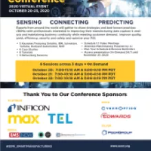
Globalized supply chains, combined with limited travel and access to experts, has led to rapid acceleration in implementations of smart manufacturing strategies. These systems are focused on improving things such as:

  • Quality and yield
  • Efficiency
  • Security and safety
  • Optimizing manufacturing cost

This inaugural Global SEMI Smart Manufacturing event brought together experts around the world to share strategies and best practices for professionals improving their manufacturing data capture & analysis and maintaining business continuity, while meeting increasing demands of customers.

The Virtual Conference includes:

  • 6 Keynotes 
  • 6 Tutorials
  • 6 Case Studies

Want to hear about all of our Smart Manufacturing Activities?  Register for the Interest List.

For more information contact Ayo Kajopaiye at [email protected].

United States

Opening Keynotes

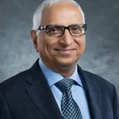
Ajit Manocha
Ajit Manocha
CEO
SEMI

Welcome Remarks

Bobby Mitra
Bobby Mitra
Worldwide Director Smart Manufacturing
Texas Instruments

Conference Opening Address: Smart Manufacturing - Capturing the ROI

Ben Dollar
Ben Dollar
Principal, Smart Operations Platform Leader
Deloitte

Conference Keynote - The State of Smart Manufacturing and Potential Global Impact

Sensing

Stéphane Piat Pic
Stéphane Piat
Senior Vice President, Quality and Supply Chain
Schneider Electric

Sensing 1 Keynote - Tailored, Connected & Sustainable 4.0 supply chain : A testimony from Schneider Electric

Antoine Dupret
Antoine Dupret
Technical expert, Research DIrector, Leti Fellow
CEA-Leti

Sensing 1 Tutorial - Integrated Sensors : how leveraging the endless miniaturization to tackle the challenges of acquisition

Vidya Vijay
Vidya Vijay
Senior Program Manager
CyberOptics

Sensing 1 Case Study - Improving Yields and Tool Uptime with Relative Humidity Sensor in Semiconductor Environments

Hattori-san
Ryuhichiroh Hattori
Partner
IBM

Sensing 2 - Keynote - Sensors Applications in Smart Factory Architecture

Choudrey TDK
Sahil Choudhary
Product Marketing Manager, IoT Sensors
TDK Invensense

Sensing 2 Tutorial - Using a Multi-Sensor wireless module for IoT applications

Lakeman-Macgearailt
Steve Lakeman & Niall Macgearailt
Senior Director of Business Development & IRAD
Inficon

Sensing 2 - Case Study - Core In Situ Sensing Technologies for Semiconductor Smart Manufacturing

Connecting

Sujeet Chand
Sujeet Chand
Chief Technical Officer & Senior Vice President
Rockwell Automation

Connecting 1 Keynote - Bringing the Connected Enterprise to Life for Semiconductor Manufacturing

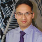
Dr. Vivek Hajarnavis
Vivek Hajarnavis
Business Development Manager - Technology Adoption
Rockwell Automation

Connecting 1 - Tutorial - The Networking Journey: From Fieldbus to the Connected Enterprise

Janus-Waldemar
Dr. Michel Janus & Dr. Waldemar Smirnov
Manufacturing Digitalization - Simulation and WIP-Flow Optimization
Bosch

Connecting 1 - Case Study - Big Data Analytics and AI Deployment in Semiconductor Manufacturing

Egashira
Ayako Egashira
Executive General Manager of Robotics Operations
Yamaha Motor

Connecting 2 Keynote - Intelligent Factory Proposed by Yamaha Motor

Dr. Daehan Won
Dr. Daehan Won & Dr. Sangwon Yoon
Assistant Professor & Professor
SUNY Binghamton

Connecting 2 - Tutorial - Digital Transformation using Artificial Intelligence/Machine Learning in the Electronics Manufacturing

Manoj Betawar
Manoj Betawar
Co-founder & CTO
Sapphire Automation

Connecting 2 - Case Study - The Smart way to Enable the Connection of Legacy Equipment

Predicting

Steve Frezon
Steve Frezon
Senior Vice President of Front End Operations
NXP

Predicting 1 - Keynote - Predict & Prevent – Automotive Semiconductor Zero Defect Enablement

Stéphane Dauzère-Pérès
Professor
Mines Saint-Etienne France

Predicting 1 Tutorial - Planning, Qualification Management and Scheduling in Semiconductor Manufacturing

Ian Pic
Ian Bone
Industrial Engineering Manager
Broadcom

Predicting 1 Case Study - Application of the Digital Twin: Automated Prediction in a Manual Factory

Koen
Koen de Backer
VP, Smart Manufacturing and Artificial Intelligence
Micron

Predicting 2 - Keynote - Smart Manufacturing & AI to drive productivity, quality & yield improvements

Professor Jang
Young Jae Jang
Professor
KAIST

Predicting 2 - Tutorial: Smart Factory – Robot Collaboration Intelligence with AI

Generic profile
James Na & Stewart Chalmers
BISTel

Case Study Presentation - AI-based Asset Management: Fast-track Continuous Improvement for Semiconductor Manufacturers

On-Demand Presentations

Kim Picture
Hyungsu Kim
President & CEO
Doople

EDA (Equipment Data Acquisition) Beyond Standard Interface

- FOA ITL Standards

The [LIVE] event is over, but the presentations and content remains fresh and applicable via the ON DEMAND platform.  To access the information, just register for the event and click on the Agenda for access to the presentations.

Content available until November 23, 2020

12:00 am - 12:00 am Off Add to Calendar Disabled America/Los_Angeles
Event format

ESPOO, Finland, 31st August 2020 – Picosun Group’s growth strategy is based on strong expansion into industrial ALD markets. To support this strategy, special emphasis has been placed on strengthening the Group’s global service organization. The investment has paid itself back in the form of high level of customer satisfaction, despite the challenges caused by the global covid-19 pandemic especially in traveling and logistics.

“Due to the reinforced localization of our service and support units, our service engineers’ utilization level has been more than 85% in the past six months, and with the latest remote service and support tools we have gained advantage to manage our customers’ PICOSUN® ALD system commissionings online and in time. ALD tool maintenances, process development, spare parts and other critical deliveries are also provided locally with maximum safety precautions in place, to ensure customers continuous operation of their PICOSUN® ALD equipment,” states Mr. Timo Malinen, Customer Experience Director of Picosun Group.

During the last months, Picosun Group has hired and trained several new service engineers and sales and support personnel to provide local support at the Group’s US, Asian, and European locations. Remote diagnostics, control, and data logging features for remote troubleshooting and process optimization of customers’ PICOSUN® ALD tools are a routine approach in the Group’s ALD solution deliveries. Augmented and/or virtual reality solutions for even more efficient service operations and remote learning/e-training possibilities are also under development and will be introduced in all Picosun’s operations later on.

“Our principle of ‘AGILE ALD’ and our position as the technological forerunner in our field obligate us to provide the best possible services and solutions to our customers. As a globally operating company, pandemic risk scenarios are an integral part of our continuous risk planning. Against the backdrop of the current covid-19 outbreak, our service operations are continuously being adapted to mitigate potential impacts. Picosun Group follows a holistic management process that enables constant development of our customer service unit to ensure the best possible response even in an emergency situation,” continues Malinen.

For Picosun, the health of employees and customers is the highest priority. In order to closely monitor and manage the covid-19 situation, Picosun follows all the safety regulations provided by WHO, CDC, ECDC, and Finnish Institute for Health and Welfare, and provides the necessary information timely to all employees, customers, and other stakeholders.

Picosun provides the most advanced AGILE ALD® (Atomic Layer Deposition) thin film coating solutions for global industries. Picosun’s ALD solutions enable technological leap into the future, with turn-key production processes and unmatched, pioneering expertise in the field – dating back to the invention of the technology itself. Today, PICOSUN® ALD equipment are in daily manufacturing use in numerous leading industries around the world. Picosun is based in Finland, with subsidiaries in Germany, USA, Singapore, Taiwan, China, Korea and Japan, offices in India and France, and a world-wide sales and support network. Visit www.picosun.com.

More information:
Mr. Timo Malinen
Customer Experience Director, Picosun Group
Tel. +358 40 5011 860
Email: [email protected]
Web: www.picosun.com

Registration

Registration

Pre-registration period: Sep 1 (Tue) - Oct 15 (Tue), 2020

Registration fee

  • SEMI members / Student: KRW 250,000
  • Non-members: KRW 300,000


Registration
South Korea Square-banner(1000-1000).jpg Business Technical


SPONSORS

Merck.png
Wonik Materials.png
Dupont.png
Dongwoo Fine-chem.png
Air Liquide.png
KCTECH.png
Entegris.png
SK Materials.png
Mecaro.png
 

  Sponsorship Opportunities: JoAnn Lee([email protected])


NOTICE

  • Presentation files agreed by speakers will be provided to attendees. It will be informed how to download the files after the event.
  • The agenda will be subject to change without notice.
  • Live session will start Oct 19, 2:00pm.
  • On-demand Session is accessible during Oct 19 - 20.


CONTACT

  Sera Jung(+82-2-531-7831 / [email protected])

SMC Korea 2019 Photos

Room 401, COEX, Seoul
Gangnam-gu
Seoul
South Korea

Live Session (10/19)

2:00 pm - 2:05 pm

Welcome

2:05 pm - 2:35 pm
Cheol Seong Hwang.jpg
Cheol Seong Hwang
Seoul National University

[Keynote] New Materials for Futuristic Semiconductor Memory Devices

2:35 pm - 3:05 pm
Dae Hyun Kim
PricewaterhouseCoopers Consulting

[Keynote] Digitalized R&D

3:05 pm - 3:35 pm
Ryoung-han Kim.jpg
Ryoung-han Kim
imec

[Keynote] On the Horizon of Semiconductor Scaling Paradigm Change and its Impact on Patterning and Materials

3:35 pm - 4:00 pm

Break

4:00 pm - 4:30 pm
Hyungsoon Park
SK hynix

[Collaboration] Technology Trends of Materials for Semiconductor Manufacturing

4:30 pm - 5:00 pm
Samjong Choi.jpg
Sam Jong Choi
Samsung Electronics

[Collaboration] Continuous Quality Improvement Strategy for Semiconductor Material SCM

On-demand Session(10/19-20)

Jeff Gambino.jpg
Jeff Gambino
On Semiconductor

[SMART Applications] CMOS Image Sensors: Challenges and Opportunities

Seong-yong Moon.jpg
Seong-yong Moon
FST

[Advanced Patterning] EUV Pellicle Development Status

Adnrew Grenville.jpg
Andrew Grenville
Inpria

[Advanced Patterning] Delivering Metal Oxide Photoresists for EUV: Overcoming Challenges to Scaling

Heejun Yang.png
Heejun Yang
Entegris

[Advanced Patterning] Lithography Filtration Innovation for Increased Yield

Mark Thirsk.jpg
Mark Thirsk
Linx Consulting

[More than Moore] Needs and Opportunities for Electronics Materials in the Coming Super Cycle

Jan Vardaman.jpg
E. Jan Vardaman
TechSearch International

[More than Moore] Advanced Packaging for Heterogeneous Integration: What’s Next

Chanho Kim.png
Chanho Kim
Air Liquide Advanced Materials

[More than Moore] Economic Considerations for ALD Precursor Selection

[NOTICE] Due to the Social Distancing for preventing COVID-19, SEMI decided to hold SMC Korea 2020 as a Virtual Event.


Materials Driving Transformation of Industry

With advanced materials now a critical enabler of semiconductor growth applications, industry leaders have emphasized significance of innovation in materials. SMC Korea 2020, the premier conference on electronic materials, will gather top executives from every segment of semiconductor manufacturing to provide the most up-to-date developments in areas of advanced materials.
Join us at SMC Korea 2020 to advance your knowledges and network with the global leaders and professionals.

9:00 am - 5:40 pm Off Add to Calendar 2020-10-19 09:00:00 2020-10-19 17:40:00 SMC KOREA 2020 [NOTICE] Due to the Social Distancing for preventing COVID-19, SEMI decided to hold SMC Korea 2020 as a Virtual Event.   Materials Driving Transformation of Industry With advanced materials now a critical enabler of semiconductor growth applications, industry leaders have emphasized significance of innovation in materials. SMC Korea 2020, the premier conference on electronic materials, will gather top executives from every segment of semiconductor manufacturing to provide the most up-to-date developments in areas of advanced materials. Join us at SMC Korea 2020 to advance your knowledges and network with the global leaders and professionals. Room 401, COEX, Seoul Gangnam-gu Seoul South Korea SEMI.org [email protected] Asia/Seoul public Asia/Seoul

Registration

Registration

Pre-registration Due Date: Aug 31 (Mon), 2020

Registration fee

  • Student: KRW 200,000
  • SEMI members: KRW 200,000
  • Non-members: KRW 250,000
Registration
South Korea MEMS&SENSOR_FORUM_banner_2020.08.20.jpg Technical

SPONSORS

EVG
Samyong S&C

  Sponsorship Opportunities: JoAnn Lee([email protected])


CONTACT

 Sera Jung(+82-2-531-7831 / [email protected])

Virtual
South Korea

9:00 am - 9:05 am

Welcome

9:05 am - 9:35 am
Keynote. Andrea Onetti.jpg
Andrea Onetti
STMicroelectronics

Keynote: Megatrend of MEMS & Sensor Industry

Session 1: Smart Applications

9:35 am - 10:05 am
S1_2. Kang-Won Lee.jpg
Kang-Won Lee
SK Telecom

Challenges and Opportunities of 5G Mobile Edge Cloud

10:05 am - 10:25 am

Break

Session 2: Smart Mobility

10:25 am - 10:55 am
S2_1. Frank Mack_0.jpg
Frank Mack
Robert Bosch

Automated Driving – Shaping the Future of Mobility

10:55 am - 11:25 am
S2_2. Jooil Park.jpg
Jooil Park
Infineon Technologies

Automotive Sensor Trend by EV

11:25 am - 11:55 pm
S2_3. Wonsik Jang.jpg
Wonsik Jang
Continental Automotive

Evolution of Vehicle EE Architecture – Impact on Electronics

11:55 pm - 1:00 pm

Lunch

Session 3: Core Technologies

1:00 pm - 1:30 pm
S3_1. John Kim.jpg
John Kim
Silex Microsystems

Efficient Sizing Up a MEMS Foundry

1:30 pm - 2:00 pm
S3_2. David Haynes.jpg
David Haynes
Lam Research

Enabling Better MEMS from Concept to High Volume Production

2:00 pm - 2:30 pm
S3_3. Dave Monk.jpg
Dave Monk
NXP Semiconductors

Advancing Quality & Reliability of MEMS for Security & Safety Applications

2:30 pm - 2:50 pm

Break

2:50 pm - 3:20 pm
S3_4. Minhyun Jung.jpg
Minhyun Jung
DB HiTek

Development of High-end Capacitive MEMS Microphone for SNR 65dB

3:20 pm - 3:50 pm
S3_5. JongDae Jung.jpg
JongDae Jung
Amkor Technology

Challenges of Optical Sensors Packaging Technologies

3:50 pm - 4:20 pm
S3_6. Sooho Bae.jpg
Sooho Bae
i3System

MEMS Infrared Sensor and Systems for Preventing COVID-19 Epidemic

4:20 pm - 4:50 pm
S3_7. Mark Da Silva.jpg
Mark Da Silva
Knowles

Specialized Mics and Processors for Creating Audio Intelligence at the Edge

MSIG

[NOTICE] Due to the Social Distancing for preventing COVID-19, SEMI decided to hold MEMS & SENSOR FORUM 2020 as a Virtual Event.

  • Presentations will be live-streamed only on Wednesday, September 2. 
  • How to access to the Online Forum will be informed to the registrants.
  • Translation will not be provided.


SENSE & CONNECT

MEMS & Sensor Forum is one-day event, intended to boost the MEMS & Sensor industry and create effective network among Korean MEMS & Sensor industry leaders.
In this forum, you can hear not only the latest technologies but also global market trends from key players.
Join this must-attend event to expand your knowledge and business networks.

9:00 am - 4:50 pm Off Add to Calendar 2020-09-02 09:00:00 2020-09-02 16:50:00 MEMS & Sensor Forum 2020 [NOTICE] Due to the Social Distancing for preventing COVID-19, SEMI decided to hold MEMS & SENSOR FORUM 2020 as a Virtual Event. Presentations will be live-streamed only on Wednesday, September 2.  How to access to the Online Forum will be informed to the registrants. Translation will not be provided.   SENSE & CONNECT MEMS & Sensor Forum is one-day event, intended to boost the MEMS & Sensor industry and create effective network among Korean MEMS & Sensor industry leaders. In this forum, you can hear not only the latest technologies but also global market trends from key players. Join this must-attend event to expand your knowledge and business networks. Virtual South Korea SEMI.org [email protected] Asia/Seoul public Asia/Seoul