Standardizing the Semiconductor Manufacturing Backend
About Collaborative Alliance of Semiconductor Test (CAST)
CAST serves SEMI members and other stakeholders in the semiconductor test area. CAST members include leaders from automated test equipment (ATE) companies, fabless, IDMs, and OSAT companies. CAST members work with their customers, suppliers, and industry colleagues to develop industry standards that reduce costs and spur innovation.
Unlike the semiconductor ‘frontend’, the ‘backend’ has little standardization with lots of different interfaces and behaviors between different equipment suppliers. How can we standardize it and gain the efficiencies that standards brought to the frontend? SEMI has several standards suites that could be used depending on the customer’s needs, including SECS/GEM, EDA/Interface A and RITdb. This webinar will describe the benefits of each, as well discuss challenges around traceability and other issues commonly encountered in the backend, and how standards can benefit the equipment users.
United States
3:00 pm
-
3:05 pm
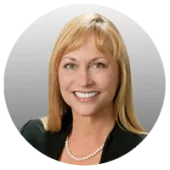
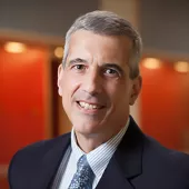
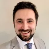
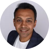
Alan Weber
Vice President, New Product Innovations
Cimetrix
Opening Remarks
Alan Weber is currently the Vice President, New Product Innovations for Cimetrix Incorporated. Previously he served on the Board of Directors for eight years before joining the company as a full-time employee in 2011.
Alan has been a part of the semiconductor and manufacturing automation industries for over 40 years. He holds bachelor's and master's degrees in Electrical Engineering from Rice University.
3:05 pm
-
3:15 pm
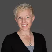
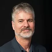
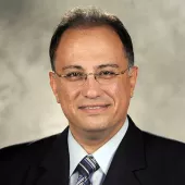
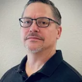
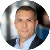
Brian Rubow
Director of Solutions Engineering
Cimetrix
SECS/GEM
Brian Rubow is the Director of Solutions Engineering for Cimetrix. He is well-known within the industry due to his involvement with the SEMI standards committees. He currently serves as the co-chairs for the North America Information and Control Committee, the North America GEM300 Task Force, and the North America DDA Task Force. Rubow has both a bachelor’s and a master’s in engineering from Brigham Young University.
3:15 pm
-
3:25 pm
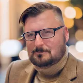
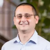
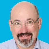
Albert Fuchigami
Senior Software Developer
PEER Group
EDA/Interface A
Albert Fuchigami is a senior software developer at PEER Group Inc. and has spent more than 20 years helping semiconductor OEMs integrate their equipment into factories around the world. He is a globally recognized leader in the SEMI Standards Program, co-leads the North America Data Diagnostic Acquisition (DDA) Task Force, and contributes to the Information & Control Technical Committee. Albert enjoys demonstrating how standards can maximize data communication with factory host systems and is a champion for integrating HTTP/2 with gRPC and Protocol Buffers technology into the Equipment Data Acquisition (EDA) / Interface A standards. He holds a Bachelor of Mathematics (Computer Science) degree from the University of Waterloo.
3:25 pm
-
3:35 pm
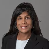
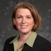
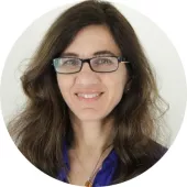
Stacy Ajouri
Senior Member of Technical
Texas Instruments
Mark Roos
CEO
Roos Instruments
RITdB
Stacy Ajouri is a Senior Member of Technical Staff at Texas Instruments in the Test Technology Group. She is the co-chair of the North America Automated Test Equipment (ATE) Technical Committee and the RITdb Task Force. She has over 30 years of experience across multiple disciplines related to test and test operations. Pulling from that experience, she supports the implementation of RITdb proof of concepts (POCs) focusing what is needed by the manufacturing and engineering community.
Mark Roos is CEO of Roos Instruments, a longtime producer of semiconductor ATE. He co-chairs the North America ATE Technical Committee and the RITdb Task Force. Roos has been involved in standards development for ATE for the past 20 years. He is currently heavily involved in the focus of RITdb POCs on scaling and latency.
3:35 pm
-
3:45 pm
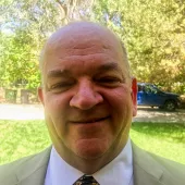
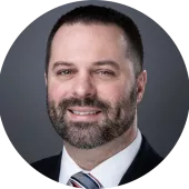
Dave Huntley
Product Manager Assembly Products
PDF Solutions
Traceability and E142
Dave Huntley was the founder and president of KINESYS Software in 1992 which developed the Assembly Line Production Supervisor (ALPS). PDF Solutions acquired the ALPS in 2017 and Dave now works in Strategic Marketing, Business Development & Standards Liaison focused on defect / process tracking and single device traceability across the supply chain.
He has a long history working with SEMI. He was co-lead of the Sort Map task force responsible for the SEMI E142 Specification for Substrate Mapping Standard. Dave is now the co-lead for the Traceability committee and two SEMI task forces; 1) Advanced Backend Factory Integration working on applying and extending wafer fab automation standards to assembly and test and 2) Single Device Traceability task force working on blockchain traceability for the supply chain.
Standardizing the Semiconductor Manufacturing Backend
Taming the Wild West of Semiconductor Backend Manufacturing
3:00-4:00 PM (PT)
Zoom
A CAST technology community webinar
3:00 pm - 4:00 pm
Off
Add to Calendar2024-02-22 15:00:002024-02-22 16:00:00Standardizing the Semiconductor Manufacturing BackendUnited StatesSEMI.org[email protected]America/Los_Angelespublic
America/Los_Angeles
About Collaborative Alliance of Semiconductor Test (CAST)
CAST serves SEMI members and other stakeholders in the semiconductor test area. CAST members include leaders from automated test equipment (ATE) companies, fabless, IDMs, and OSAT companies. CAST members work with their customers, suppliers, and industry colleagues to develop industry standards that reduce costs and spur innovation.
2024 Technology Workshops Enabling the Future of Electronics
Registration
Registration Fee (April 16 & 17 only)
$250 members $399 non-members
SEMI members who wish to join the NextFlex Workshop on April 19th should contact [email protected] for a special discount code.
Cancellation Policy
Cancellations received on or before March 16, 2024, are fully refunded with a $50 processing fee. Refunds will not be issued for cancellations (including no-shows) made after March 16, 2024, and only substitutions are accepted with a written note from the registered attendee. Please email your cancellations or substitutions on company letterhead to Michelle Fabiano at [email protected].
4610 Vestal Pkwy E, Vestal, NY 13850 TEL: (607) 770-8500
SEMI NBMC Technical Gap Analysis Workshop - Tues. 4/16 - 8 am-6 pm During this workshop, attendees will address the technical topics / gaps in the Nano-Bio Materials space to explore topics and technology development required to meet development objectives. Breakfast, and lunch will be included and reception at the end of the day will be included.
SEMI FlexTech FHE Technical Gap Analysis Workshop - Wed. 4/17 - 8 am-4 pm, followed by tours of Binghamton University labs Attendees will then turn their sights to completing a Technical Gap Analysis in preparation for FlexTech’s next Request for Proposals (RFP), including exploring topics and technology development required to meet development objectives. Breakfast, lunch and tours of Binghamton University lab tours will conclude the day.
Binghamton University Tours - Wed. 4/17 - 4:00pm - 5:30pm The tour will include facilities that are part of the S3IP (Small Scale Systems Integration & Packaging) a New York State Center of Excellence, CAMM (Center for Advanced Microelectronics Manufacturing) a New York State Center of Advanced Technology and home to the New York Node of NextFlex, the Analytical & Diagnostics Laboratory, the IEEC (Integrated Electronics Engineering Center) a New York State Center of Advanced Technology and NECCES (the Northeast Center for Chemical Energy Storage).
Binghamton University 2024 Art of Science Exhibit - Wed. 4/17 - 4:00pm - 5:30pm Binghamton University holds an annual contest that celebrates the beauty of science through photographs and images that describe some aspect of research and captured visually. The advances in imaging technology and tools mean that scientists have an increased ability to generate exciting data as well as to create compelling works of art and workshop attendees are invited to the opening reception for the 2024 Art of Science Exhibit in the atrium of the Center of Excellence Building. Contest winners will be announced, and refreshments will be served.
In addition: NextFlex Workshop– Thurs, 4/18 NextFlex will convene the hybrid electronics community for a one-day workshop at Binghamton University in New York on April 18 to explore and define collaborative responses to soon to be announced opportunities under the CHIPS and Science Act, including the National Advanced Packaging Manufacturing Program (NAPMP), with a specific focus on advancing hybrid electronics for industrial and medical applications.
Attendees will break into groups for smaller discussions to identify challenges, prioritize those challenges and identify opportunities on critical issues discussed throughout the morning session.
Additively Manufactured Flexible " Smart" Packaging and Reconfigurable On-Package Antenna Arrays for Next Generation 5G/mm Wave System on Package Designs
Attendees will break into groups for smaller discussions to identify challenges, prioritize those challenges and identify opportunities on critical issues discussed throughout the morning session.
2:35 pm
-
2:50 pm
Break
2:50 pm
-
4:00 pm
Breakout Sessions Readout
4:00 pm
-
5:30 pm
Binghamton University Laboratory Tours & 2024 Art of Science Exhibit and Reception
The tour will include facilities that are part of the S3IP (Small Scale Systems Integration & Packaging) a New York State Center of Excellence, CAMM (Center for Advanced Microelectronics Manufacturing) a New York State Center of Advanced Technology and home to the New York Node of NextFlex, the Analytical & Diagnostics Laboratory, the IEEC (Integrated Electronics Engineering Center) a New York State Center of Advanced Technology and NECCES (the Northeast Center for Chemical Energy Storage).
Join leaders from FlexTech, NBMC, NextFlex and the microelectronics industry in this dynamic workshop, where we'll explore advancements, challenges, and solutions in critical technologies like flexible hybrid electronics, hybrid electronics, wearables, bio-signal sensing for real-time cognitive and physical state monitoring, and more. Participate in hands-on sessions, cross-disciplinary discussions, and gain insights from industry and academia through impactful talks. Contribute your suggestions in dynamic breakout sessions to shape and enable the future of these technologies.
2024 Technology Workshops Enabling the Future of Electronics
- NBMC Gap Analysis
- FHE Gap Analysis
- NextFlex Workshop (April 18 - separate registration)
7:30 am - 6:00 pm
Off
Add to Calendar2024-04-16 07:30:002024-04-17 18:00:002024 Technology Workshops Enabling the Future of ElectronicsPresented by Hosted by Join leaders from FlexTech, NBMC, NextFlex and the microelectronics industry in this dynamic workshop, where we'll explore advancements, challenges, and solutions in critical technologies like flexible hybrid electronics, hybrid electronics, wearables, bio-signal sensing for real-time cognitive and physical state monitoring, and more. Participate in hands-on sessions, cross-disciplinary discussions, and gain insights from industry and academia through impactful talks. Contribute your suggestions in dynamic breakout sessions to shape and enable the future of these technologies.Binghamton University, Innovative Technologies Complex (ITC) 85 Murray Hill Rd Vestal, NY 13850 United StatesSEMI.org[email protected]America/Los_Angelespublic
Event Contact
For questions, please contact Michelle Fabiano at [email protected].
Evolution of IC Packaging – Fan-in, Fan-out WLP, Embedded Packaging technology, System on Chip (SOC), System in Package (SiP), 3D IC, WLP, TSV etc.
Principles of Interconnects ranging from TAB, Wirebond to various Flip Chip bonding such as thermocompression bonding with NCP, C4, ACF for manufacturing and R&D development
Board level assembly and its soldering materials and failure mechanisms for 2nd level interconnect
Overview of interposer of lead frame, ceramic, flex to BT substrates for Microelectronics Packaging
Assembly flow and new assembly techniques such as stealth dicing, compression molding, underfill molding etc., and its assembly materials for Microelectronics packaging
Material characterization from bulk to interfaces for Microelectronics packaging
Why should I attend?
Gain technical knowledge for industry professionals
Enhance knowledge in manufacturing and R&D know-how in IC packaging
Apply Key Technical Concepts in Problem Solving through Real Case Studies
Networking opportunities with industry peers
Who should attend?
Beneficial for directors, managers, process & equipment engineers, R&D engineers and Quality & Reliability engineers working in the areas of microelectronics packaging
Useful for sale or application engineers who supply packaging materials and tools to the industry
Royale Chulan Penang No 1 & 2, Pengkalan Weld, Georgetown 10300Penang Pulau Pinang Malaysia
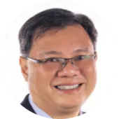
MEET OUR SPEAKER
Dr. Lee Teck Kheng
Director, Technology Development Centre, Institute of Technical Education Singapore,
SEMI SEA Advance Packaging Technical Committee Member
9:00 am
Introduction to IC Packaging & Interconnects
Introduction to IC Packaging
• Functions of Packaging – Mechanical, Material, Electrical and Chemical
• Review of Packaging Trend – BGA, CSP, Fan-in & Fan-out WLP, 3D Packaging, SoC vs SiP etc
• Challenges in Assembly and Packaging
Board Assembly and Soldering & PCB and IC Carriers
Board Assembly and Soldering
• Through Hole & SMT – Stencil Print Process, Reflow Profile
• Solder Materials – Alloy, Flux, Solvents, self-alignment effect
• Pb Free Solder – Ternary phase diagram, SnAgCu
• Intermetallics and Growth – Diffusion mechanism, Arrhenius equation
• Testing and Reliability – Ball shear & pull failure strength and modes, Fatigue, Weibull distribution
PCB and IC Carriers
• PCB Technology – Material properties, PCB fabrication process, drilling, patterning, plating, solder resist, laminating
• IC Carriers – Design rule, Leadframe, LTCC, Flex and BT substrates
• Substrate Development
4:00 pm
Q&A | Case Studies
5:00 pm
End of Day 1
9:00 am
Assembly Process
• Thickness Reduction – Grinding, Lapping, Polishing, CMP
• Dicing/Singulation – Blade, Laser, Stealth dicing, Dicing after grind
• Die Attach – Eutectic bonding, DA materials, Collets
• Plasma – Argon, Oxygen plasma, Surface tension
• Encapsulation – Mold constitutes and properties, Transfer, Film and compression molding, Dam and fill
• Plating – Solder plating, NiPd finish, PPF
• Trim & Form – ESD, Lead formation, Spring back mechanism
Usual Member Rate: SGD 750 Usual Non-member Rate: SGD 935
*The above rates are inclusive of coffee/tea breaks and luncheon for both days
Register before 23 February 2024 to enjoy Early Bird rate of 15% off the above rates.
A certificate of completion will be awarded at the end of the seminar.
*Malaysian Companies - HRDC Claimable for Penang Business Summit Seminar 1: Advanced Packaging (Advanced Packaging and Material Characterization) (subject to T&C, please contact HRDC for more information). For HRDC claims, please refer to the following links on the claiming matrix and guidelines:
Off
Add to Calendar2024-03-06 00:00:002024-03-07 00:00:00Penang Business Summit Seminar 1: Advanced PackagingAdvanced Packaging and Material Characterization*Note: Seminar 1 and Seminar 2 timing will overlap on 7 Mar Participating Fee:Usual Member Rate: SGD 750 Usual Non-member Rate: SGD 935 *The above rates are inclusive of coffee/tea breaks and luncheon for both daysRegister before 23 February 2024 to enjoy Early Bird rate of 15% off the above rates. A certificate of completion will be awarded at the end of the seminar. *Malaysian Companies - HRDC Claimable for Penang Business Summit Seminar 1: Advanced Packaging (Advanced Packaging and Material Characterization) (subject to T&C, please contact HRDC for more information).For HRDC claims, please refer to the following links on the claiming matrix and guidelines:HRDC Approval Letter for Penang Business SummitAllowable Cost MatrixHRDC SBL Grant HelperHRDC SBL Claim Helper Contact us for enquiries!For Program: Ms. Cecelia Fong | [email protected] | +65.9750.2382 For Registration / HRDC Claims: Ms. Gillian Lim | [email protected] | +65.9048.1123 Royale Chulan Penang No 1 & 2, Pengkalan Weld, Georgetown 10300 Penang Pulau Pinang MalaysiaSEMI.org[email protected]Asia/Kuala_Lumpurpublic
Asia/Kuala_Lumpur
SOLD OUT
2024 EHS Summit
Registration Details
Registration is required for this event as it is likely to reach maximum room capacity, at which point interested attendees will be waitlisted.
SEMI Members: $100
Non-Members of SEMI: $150
Refunds possible before January 10, 2024. Substitutions allowed up to January 24.
The Summit includes strategic business and technical information for many levels and sectors of the ecosystem, including:
Government relations/advocacy staff
EHS regulatory professionals
Senior executives
Business development
Device manufacturers
Equipment suppliers
Materials suppliers
Component suppliers
Fab and facility systems construction companies
SEMI 673 South Milpitas Avenue Milpitas, CA95035 United States
8:30 am
-
9:00 am
Registration & Networking
9:00 am
-
9:05 am
James Amano
Senior Director, EHS
SEMI
Welcome
9:05 am
-
9:20 am
James Amano
Sr. Director, EHS
SEMI
Europe PFAS Restriction Proposal
9:20 am
-
9:45 am
Russ LaMotte
Principal
Beveridge & Diamond PC
US EPA PFAS Reporting rule
9:45 am
-
10:10 am
Andrew Petraszak
Tokyo Electron
Ben Kallen
SEMI
PFAS US States Proposals & Positions
10:10 am
-
10:30 am
Break
10:30 am
-
11:00 am
Lauren Crane
Lam Research
European Regulations
Including: EU Machinery Regulation, Battery Regulation, Cybersecurity Resiliency Act (CRA), AI regulation, the Ecodesign “passport” concept. UK Conformity Assessed (UKCA) mark. California fan efficiency regulation. SEMI EHS Standards update.
11:00 am
-
11:25 am
Allen Karpman
Arkema
AIM Act: HFC Allocations
11:25 am
-
11:50 am
Kristine Baranski, PE
Global Air Program Manager
Intel
AIM Act: challenges with new refrigerants
11:50 am
-
12:10 pm
Katelyn Walck
Chemours
James Snow
SCREEN
SIA PFAS Consortium
12:10 pm
-
1:15 pm
Lunch & Networking
1:15 pm
-
1:35 pm
James Amano
SEMI
SEMI PFAS Initiative
1:35 pm
-
2:00 pm
Russ LaMotte
Principal
Beveridge & Diamond
TSCA PBT: PIP, DecaBDE, What's Next?
2:00 pm
-
2:35 pm
Ben Gross
Applied Materials
Supika Mashiro
TEL
Katelyn Walck
Chemours
Lauren Crane
Lam Research
Supply Chain Inquiry Panel - sharing best practices
Plan now to join fellow semiconductor industry professionals at SEMI Headquarters in Milpitas, California for presentations and discussions around critical EHS regulatory issues impacting the industry.
Industry experts will address regulations in Europe and the United States that could significantly threaten our capability to continue manufacturing. Topics will include:
US EPA PFAS Reporting Rule
US AIM Act HFC phasedown: challenges with new refrigerants
Updates from SEMI PFAS Initiative and other collaborative industry efforts.
US EPA TSCA: PIP 3:1, DecaBDE…what's next?
Panel discussion on supply chain communication.
Plan now to attend, network and strategically prepare your company. This event is offered as an in-person briefing only.
EHS Summit 2024
Regulations, Rules, Allocations & Proposals
8:30 am - 3:30 pm
Off
Add to Calendar2024-01-25 08:30:002024-01-25 15:30:002024 EHS Summit Plan now to join fellow semiconductor industry professionals at SEMI Headquarters in Milpitas, California for presentations and discussions around critical EHS regulatory issues impacting the industry.
Industry experts will address regulations in Europe and the United States that could significantly threaten our capability to continue manufacturing. Topics will include:
US EPA PFAS Reporting Rule
US AIM Act HFC phasedown: challenges with new refrigerants
US AIM Act HFC Allocation
EU: PFAS Restriction Proposal, F-gas, Revised Machinery Regulation, Revised Battery Regulation, Pending Cybersecurity resiliency regulation, Pending AI regulation, the ecodesign “passport” concept.
Updates from SEMI PFAS Initiative and other collaborative industry efforts.
US EPA TSCA: PIP 3:1, DecaBDE…what's next?
Panel discussion on supply chain communication.
Plan now to attend, network and strategically prepare your company. This event is offered as an in-person briefing only.SEMI 673 South Milpitas Avenue Milpitas, CA 95035 United StatesSEMI.org[email protected]America/Los_Angelespublic
America/Los_Angeles
-
Off
Add to Calendar2024-05-15 00:00:002024-05-17 00:00:00Key Semiconductor Account Selling & ManagementMilpitas, CA 95035 United StatesSEMI.org[email protected]America/Los_Angelespublic
-
8:00 am - 5:00 pm
Off
Add to Calendar2024-04-16 08:00:002024-04-18 17:00:00Fundamentals of Product Marketing 2.5Milpitas, CA 95035 United StatesSEMI.org[email protected]America/Los_Angelespublic
SEMI Cybersecurity Launch Workshop
Registration
Registration for this workshop is free.
For questions, please contact Mayura Padmanabhan at [email protected].
Join us for a 2-day working session to align our industry on concrete next steps to secure semiconductor manufacturing against an ever-evolving threat environment. With our complex and interconnected supply chains, no single company can be safe unless all companies are safe. Our consortium of device makers, foundries, equipment makers, component suppliers, and software suppliers are working together to rapidly develop a practical plan to improve security now, and for years to come while minimizing costs and avoiding duplication.
• Consortia governance, structure, deliverables, and roadmap for 2024
• E187 SEMI Standard implementation ideation session
• Develop a method to survey, evaluate, and certify manufacturing equipment cybersecurity protections
• Globalization of SEMI Taiwan’s E187 reference architecture and checklist
Day 2: December 7, 2023 - 8 am - 3 pm PT
8:00 am
-
3:00 pm
• Opportunities for collaboration and information sharing for cyber threats and incidents
• Supply Chain Cybersecurity working session
• Create a semiconductor industry-specific framework to measure security and implementation approach across the entire ecosystem
• Review NIST industry profiles and evaluate for suitability in semiconductor
• Next steps: Including forming working groups and assigning leaders
Join us for a 2-day workshop aimed at developing and advocating a practical, standards-based, industry-wide approach to improving cybersecurity and resilience across the semiconductor supply chain.
Time:
Day 1: Noon - 7 pm PT
Day 2: 8 am – 3 pm PT
In-person registration has reached capacity. However, you can still register to participate online.
SEMI Cybersecurity Launch Workshop
December 6-7, 2023
Off
Add to Calendar Disabled
America/Los_Angeles
Register now
Introduction to Mesoline’s Emerging 3D Micro Printing Technology, Microchannel Particle Deposition (MPD), Used for MEMS & Sensors
Mesoline’s Microchannel particle deposition (MPD) is a wafer-scale thick-film deposition process where a polymeric stamp is used to transfer ink onto a substrate. This novel microfabrication technology offers ultra-small and reproducible micro features fabricated with extensive parallelization and high scalability. Unique process features include: (1) full wafers patterning in 15-minutes, (2) 1 to 50mm structures with up to 5/1 aspect ratios and 3) full 3D-control of the printed structures. Many different sensor applications of this technology will be introduced, including: (1) printing sensing electrodes for metal oxide gas sensors, (2)printing of getters for microbolometers, (3) printing of porous electrodes for biosensing applications and (4) accurate deposition of glass frit for advanced packaging applications.
8:00 am - 9:00 am
Off
Add to Calendar2023-12-06 08:00:002023-12-06 09:00:00Mesoline’s 3D Micro Printing Technology & Microchannel Particle DepositionIntroduction to Mesoline’s Emerging 3D Micro Printing Technology, Microchannel Particle Deposition (MPD), Used for MEMS & Sensors
Mesoline’s Microchannel particle deposition (MPD) is a wafer-scale thick-film deposition process where a polymeric stamp is used to transfer ink onto a substrate. This novel microfabrication technology offers ultra-small and reproducible micro features fabricated with extensive parallelization and high scalability. Unique process features include: (1) full wafers patterning in 15-minutes, (2) 1 to 50mm structures with up to 5/1 aspect ratios and 3) full 3D-control of the printed structures. Many different sensor applications of this technology will be introduced, including: (1) printing sensing electrodes for metal oxide gas sensors, (2)printing of getters for microbolometers, (3) printing of porous electrodes for biosensing applications and (4) accurate deposition of glass frit for advanced packaging applications.United StatesSEMI.org[email protected]America/Los_Angelespublic
America/Los_Angeles
Register Now
PFAS is prevalent in our world and very much in our current conversation. But what is it? (or more correctly, what are they?), why are they under great scrutiny? are they all hazardous? and how would the semiconductor industry be impacted by their removal? With so much at stake, it is imperative that we have clarity in the discussion to ensure we successfully address this issue.
This webinar will address the what, why, and how of PFAS in the semiconductor industry. Laurie Beu, noted semiconductor EHS consultant and leader of SIA’s Semiconductor PFAS Consortium, will provide an overview of PFAS materials, concerns about health effects, and the current state of regulatory response. Laurie’s talk will be followed by Ralph Dammel, Technology Fellow at EMD Electronics, who will provide insights from a materials manufacturer’s perspective on the use of PFAS in the multiple markets addressed by EMD. He will discuss the importance of PFAS in lithography chemicals, the impact of potential new regulations, and options to reduce or eliminate the use of PFAS in semiconductor applications.
PFAS is prevalent in our world and very much in our current conversation. But what is it? (or more correctly, what are they?), why are they under great scrutiny? are they all hazardous? and how would the semiconductor industry be impacted by their removal? With so much at stake, it is imperative that we have clarity in the discussion to ensure we successfully address this issue.
Join the SEMI Electronic Materials Group (EMG) for a open conversation about the impact on the materials sector.
How can you spell semiconductors without “F” (luorine)
An EMG Webinar
10:00 am - 11:00 am
Off
Add to Calendar2023-10-18 10:00:002023-10-18 11:00:00Spelling semiconductors without “F” (luorine)PFAS is prevalent in our world and very much in our current conversation. But what is it? (or more correctly, what are they?), why are they under great scrutiny? are they all hazardous? and how would the semiconductor industry be impacted by their removal? With so much at stake, it is imperative that we have clarity in the discussion to ensure we successfully address this issue.
Join the SEMI Electronic Materials Group (EMG) for a open conversation about the impact on the materials sector.
Virtual, Online United StatesSEMI.org[email protected]America/Los_Angelespublic
America/Los_Angeles
MedTech Workshop - Navigating the Digital Health Revolution
Registration
SEMI Member: $99
Non-Members: $199
Cancellations received on or before October 30, 2023, are fully refunded with a $50 processing fee. Refunds will not be issued for cancellations (including no-shows) made after October 30, 2023, and only substitutions are accepted with a written note from the registered attendee. Please email your cancellations or substitutions on company letterhead to Michelle Fabiano at [email protected].
For questions, please contact Michelle Fabiano at [email protected].
As we witness a paradigm shift in the Healthcare Revolution – moving from a provider-centric model to one of personalized care that democratizes healthcare access - it becomes evident that the core of this transformation revolves around microelectronics and associated technologies. The "Navigating the Digital Health Revolution" workshop serves as a conduit between engineering and life sciences, emphasizing the confluence of Medicine and Digital Technology in reshaping digital healthcare.
We invite you to join this exciting workshop hosted by Merck, EMD to prepare for an increasingly intelligent future for all humanity!
Who Should Attend?
Scientists ● Entrepreneurs ● Microelectronics engineers ● Data analysts ● Broader community of MedTech innovators
Why Attend?
Identify industry challenges (such as Data Transparency, Technology Limitations, Supply Chain Weaknesses, Regulatory Challenges, Cybersecurity)
Prioritize these challenges.
Identify solutions that are better addressed collectively.
Develop an execution plan for these solutions.
EMD Serono Research Center 45 A Middlesex Turnpike Room: Three Sisters (Photo ID or passport needed for check-in) Billerica, MA01821 United States
Attendees will break into groups for smaller discussions to identify challenges, prioritize those challenges and identify opportunities on critical issues discussed throughout the day which may include the role of AI in MedTech, data security and privacy in digital health and emerging technologies in MedTech.
Topics:
1. Electronics Supply Chain for Medical Applications
2. Data, AI & Cyber Security
3. Bridging the Gap Between Electronics & Medical Device Technology
3:00 pm
-
3:15 pm
Break
3:15 pm
-
4:00 pm
Breakout Sessions Readout
4:00 pm
-
5:30 pm
Networking Reception
Join us for a one-day MedTech workshop to explore the convergence of semiconductor engineering and life sciences and engage in enriching breakout sessions led by experts. Discover how industry leaders can collaborate on semiconductor-driven solutions to improve healthcare care delivery to everyone, everywhere.
Please note that seats are limited to 80 attendees.
This event is organized by the SEMI Smart MedTech Initiative.
MedTech Workshop - Navigating the Digital Health Revolution
[IN-PERSON EVENT]
Thursday, November 30, 2023
7:30 AM – 5:30 PM EST
7:30 am - 5:30 pm
Off
Add to Calendar2023-11-30 07:30:002023-11-30 17:30:00MedTech Workshop - Navigating the Digital Health RevolutionJoin us for a one-day MedTech workshop to explore the convergence of semiconductor engineering and life sciences and engage in enriching breakout sessions led by experts. Discover how industry leaders can collaborate on semiconductor-driven solutions to improve healthcare care delivery to everyone, everywhere.
Please note that seats are limited to 80 attendees.
This event is organized by the SEMI Smart MedTech Initiative. EMD Serono Research Center 45 A Middlesex Turnpike Room: Three Sisters (Photo ID or passport needed for check-in) Billerica, MA 01821 United StatesSEMI.org[email protected]America/New_Yorkpublic
America/New_York
Register now