-
10:00 am - 5:00 pm
Off
Add to Calendar2023-07-13 10:00:002023-07-14 17:00:00Thailand Business Summit 2023Bang Kok ThailandSEMI.org[email protected]Asia/Bangkokpublic
Asia/Bangkok
EMG Webinar Push-Pull How Members of the Semiconductor Supply Chain Drive a Sustainable Future
In recent years, sustainability has emerged as a critical aspect of global development, demanding increased attention across industries. The semiconductor industry has a pivotal role to play in promoting environmental responsibility.
In this webinar we will hear the successes, challenges, and ongoing efforts from both a semiconductor device manufacturer and a semiconductor material supplier and how efforts across the supply chain influence each other. Join us as we foster knowledge sharing and collaborations to create a sustainable future for the semiconductor industry and the planet as a whole.
Push & Pull: How the Members of the Semiconductor Supply Chain Drive a Sustainable Future
Brought to you by the EMG Webinar Sub-Committee
10:00 am - 11:00 am
Off
Add to Calendar Disabled
America/Los_Angeles
Register
Experience the industry through Listen, Discuss, See, Touch, and Learn activities and enjoy improved job satisfaction and operational efficiency.
Session 1: The Silicon Chip
"World in a Grain of Sand" Video
Industry chronology
The development of electronics from the thermionic valve to complex ICs
Semiconductor family tree
IC types (logic, memory, microprocessors)
Session 2: Basic Electronics
Introduction to electronics theory
Binary language & ASCII code
Semiconductor materials & their operation
The p-n junction & transistor operation
Boolean algebra & digital logic explained
Session 3: Semiconductor Manufacture
Industry structure
Polysilicon & silicon water production
Wafer fab/front-end process
Back-end (wafer probe, assembly, final test & finishing) operations
"Silicon Chip" video
Session 4: Economics of IC Manufacture
Wafer fab investment trends
Cost structure & cost models
Process yields & manufacturing defects
Die size & cost reduction issues
Back-end cost elements
Typical device costs
Session 5: IC Market Overview
Market segmentation
Company size
Packaging & technology trends
Industry learning curve
Industry cyclicality
Industry dynamics
Market outlook
Session 6: The IT Revolution
Impact of Information Technology
Market trends & industry outlook
Impact of microelectronics
More about the instructor:
Malcolm Penn is the founder of Future Horizons, a leading global semiconductor industry analyst. He has over 50 years’ experience in the semiconductor and electronics industry, from advanced research to manufacturing and applications.
SEMI 673 S. Milpitas Blvd Milpitas, CA95035 United States
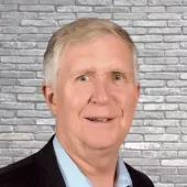
Malcolm Penn
Chairman & CEO
Future Horizons
Gain a competitive edge in the Semiconductor Industry by learning how the IC industry works from the science that enables silicon chips to be made from sand to the market fundamentals that drive applications and economics.
This workshop is relevant to technical and non-technical professionals in the semiconductor and IT industry:
Sales, marketing, business development professionals
R&D, engineers, product managers,
Purchasing managers, finance, product planners
Human resources, recruitment and industry training personnel
Government officials, public/private investors
Media, PR and advertising organizations
Attendance is limited to 40 participants.
Silicon Chip Industry Awareness Workshop
A one-day introduction to the Integrated Circuit (IC) Industry technology, manufacturing and markets
9:30 am - 4:00 pm
Off
Add to Calendar2023-05-15 09:30:002023-05-15 16:00:00Silicon Chip Industry Awareness WorkshopGain a competitive edge in the Semiconductor Industry by learning how the IC industry works from the science that enables silicon chips to be made from sand to the market fundamentals that drive applications and economics.
This workshop is relevant to technical and non-technical professionals in the semiconductor and IT industry:
Sales, marketing, business development professionals
R&D, engineers, product managers,
Purchasing managers, finance, product planners
Human resources, recruitment and industry training personnel
Government officials, public/private investors
Media, PR and advertising organizations
Attendance is limited to 40 participants.
SEMI 673 S. Milpitas Blvd Milpitas, CA 95035 United StatesSEMI.org[email protected]America/Los_Angelespublic
America/Los_Angeles
ESD Alliance Export Webinar
This webinar will be recorded. Registrants will receive a link to the recording after the event.
The discussion will help attendees understand why and how governments implement trade controls, what “exports” are and how they take place in different business contexts, and common due diligence methods – such as customer screening – that United States companies use to incorporate regulatory compliance into their business processes. Finally, the discussion will address recent regulatory updates which address current issues such as US-China trade relations and the anticipated effects of those regulations on the US semiconductor design ecosystem.
Following the presentations we will address questions from attendees as time permits.
Meet the Speakers
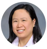
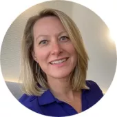
Ada Loo Group Director and Associate General Counsel, Cadence Design Systems Biography
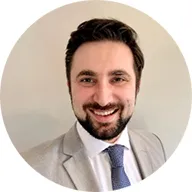
Ben Kallen Senior Manager, Public Policy & Advocacy SEMI Biography
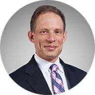
Marc Coldiron Director of Global Public Policy & Advocacy SEMI Biography
Join us as members of SEMI's Public Policy and Advocacy team will join representatives from Cadence Design Systems to host a webinar focused on export control policy—a topic which is especially relevant to the ESD Alliance given the global reach of the EDA industry. SEMI staff will contextualize export controls within the broader national political landscape and offer their perspective on what EDA companies can expect over the longer term.
ESD Alliance Export Webinar
Navigating Export Controls in EDA
June 11, 2026 | 9–10:30am PT | Virtual
9:00 am - 10:30 am
Off
Add to Calendar2026-06-11 09:00:002026-06-11 10:30:00ESD Alliance Export WebinarJoin us as members of SEMI's Public Policy and Advocacy team will join representatives from Cadence Design Systems to host a webinar focused on export control policy—a topic which is especially relevant to the ESD Alliance given the global reach of the EDA industry. SEMI staff will contextualize export controls within the broader national political landscape and offer their perspective on what EDA companies can expect over the longer term. CA United StatesSEMI.org[email protected]America/Los_Angelespublic
America/Los_Angeles
1
Join us for the annual ESDA CEO/Executive Outlook—
The evening begins at 5:30pm with a networking dinner
Special guest speakers from RISC-V International and SiFive.
Lively panel discussion with influential executives from Breker Verification Systems; D2S; Keysight; PDF Solutions, and Real Intent on the state of the system design industry plus a future industry outlook.
Keysight 5301 Stevens Creek Blvd. Building 5 Santa Clara, CA95051 United States
5:30 pm
-
6:45 pm
Registration/Networking Dinner
6:45 pm
-
6:50 pm
Bob Smith
Executive Director
ESD Alliance
Welcome and Speaker Introductions
6:50 pm
-
7:30 pm
Calista Redmond
CEO
RISC-V International
Jack Kang
SVP of Sales and Business Development
SiFive
Special Guest Speakers
7:30 pm
-
8:30 pm
Bob Smith | Moderator
Executive Director
ESD Alliance
Dave Kelf
CEO
Breker Verification Systems
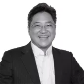
Aki Fujimura
CEO
D2S
Niels Fache
VP and GM
Keysight
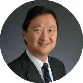
John Kibarian
CEO
PDF Solutions
Prakash Narain
CEO
Real Intent
Moderator & Panelists
Hear panelists from Breker Verification Systems | D2S |Keysight | PDF Solutions | Real Intent discuss the state of the electronic system design industry and their outlook for the coming years.
- Dave Kelf | CEO | Breker Verification Systems
- Aki Fujimura | CEO | D2S
- Niels Fache | VP and GM | Keysight
- John Kibarian | CEO | PDF Solutions
- Prakash Narain | CEO | Real Intent
ESDA CEO/Executive Outlook hosted at Keysight in Santa Clara, CA.
ESD Alliance CEO/Executive Outlook
May 9, 2024
5:30 PM - 8:30 PM
5:30 pm - 8:30 pm
Off
Add to Calendar2024-05-09 17:30:002024-05-09 20:30:00ESD Alliance CEO/Executive OutlookESDA CEO/Executive Outlook hosted at Keysight in Santa Clara, CA. Keysight 5301 Stevens Creek Blvd. Building 5 Santa Clara, CA 95051 United StatesSEMI.org[email protected]America/Los_Angelespublic
America/Los_Angeles
Register Now!
California CHIPS Act Support: State and Local Government Incentives
California CHIPS Act Support: State and Local Government Incentives
SEMI has invited the California Governor’s Office of Business and Economic Development (GO-Biz) to discuss California state services and programs that can be leveraged in alignment with current and upcoming CHIPS Funding Opportunities. GO-Biz provides direct support to semiconductor businesses of all sizes and scopes via site selection and identification services, personalized incentive navigation services, liaison services, and local engagement and environmental process assistance.
Competitive CHIPS proposals will apply one or more state or local government incentive(s) to finance their project costs. In this webinar, representatives from GO-Biz will outline different state incentives, including the R&D tax credit and Partial Sales and Use Tax Credit, that can be used to meet this financing requirement. Additionally, they will detail how their multiple services may be leveraged to strengthen your project proposal plans. Following a short presentation, they will be available for a Q&A.
Meet the Speakers
Joe Stockunas
President
SEMI Americas
Kaina Pereira
Senior Advisor, Business Development
Governor’s Office of Business and Economic Development (GO-Biz)
Michael Karavolias
Sustainable Innovation Specialist
Governor’s Office of Business and Economic Development (GO-Biz)
Derek Kirk
Assistant Deputy Secretary of Climate
California Labor & Workforce Development Agency
Co-sponsored by
This Virtual Forum is 10:00–11:00am Pacific Time
United States
Co-sponsored by SEMI and GO-Biz
The California CHIPS Act webinar will outline state programs and available state support that California applicants can leverage for more competitive CHIPS applications.
California CHIPS Act Support: State and Local Government Incentives
[VIRTUAL EVENT]
California CHIPS Act Support: State and Local Government Incentives
April 11, 2023
10:00 am - 11:00 am
Off
Add to Calendar Disabled
America/Los_Angeles
2
Register Now
The passage of the CHIPs Act and the Inflation Reduction Act have created opportunities and challenges for the semiconductor industry supply chain. Join industry professionals as we discuss the implications of this legislation and how materials companies can make the most of it.
What's In it for Materials Companies?
CHIPs Act, Inflation Reduction Act, and Tax Incentives
10:00 am - 11:00 am
Off
Add to Calendar Disabled
America/Los_Angeles
2
Substrate and PCB fabrication processes and its key processes and materials such as ABF, BT, FR5, etc.
Build-up micro-via technologies with use of lasers, plasma, photo materials etc.
Registration and tolerances of substrate design in relation to substrate and PCB fabrication processes which includes via to pattern, pattern to resist etc, which can affect microelectronics assembly processes.
Materials, design and surface finishes (Cu, NiAu, ENIG , NiPdAu etc) with respect to assembly processes and parameters.
Substrate defects and package reliability including failure of fatigue, kirkendall voids and intermetallics.
Why should I attend?
Provides necessary technical knowledge for industry professionals
Enhance knowledge in manufacturing and R&D know-how in IC packaging
Case studies discussion
Networking Opportunity with industry peers
Who should attend?
Directors, managers, process engineers, R&D engineers working in the areas of microelectronics
Useful for sale or application engineers who supply packaging materials and tools to the industry
Malaysian International Trade & Exhibition Centre (MITEC) No. 8 Jalan Dutamas 2 50480Kuala Lumpur Kuala Lumpur Malaysia
MEET OUR SPEAKER
Dr. Lee Teck Kheng
Director, Technology Development Centre, Institute of Technical Education Singapore,
SEMI SEA Advance Packaging Technical Committee Member
Note: Program is subject to changes.
9:00 am
Introduction to IC Packaging & Interconnects
Introduction to IC Packaging
• Functions of Packaging – Mechanical, Material, Electrical and Chemical
• Review of Packaging Trend – BGA, CSP, Fan-in & Fan-out WLP, 3D Packaging, SoC vs SiP etc
• Challenges in Assembly and Packaging
Board Assembly and Soldering & PCB and IC Carriers
Board Assembly and Soldering
• Through Hole & SMT – Stencil Print Process, Reflow Profile
• Solder Materials – Alloy, Flux, Solvents, self-alignment effect
• Pb Free Solder – Ternary phase diagram, SnAgCu
• Intermetallics and Growth – Diffusion mechanism, Arrhenius equation
• Testing and Reliability – Ball shear & pull failure strength and modes, Fatigue, Weibull distribution
PCB and IC Carriers
• PCB Technology – Material properties, PCB fabrication process, drilling, patterning, plating, solder resist, laminating
• IC Carriers – Design rule, Leadframe, LTCC, Flex and BT substrates
• Substrate Development
4:00 pm
Q&A | Case Studies
5:00 pm
End of Day 1
5:00 pm
End of Day 1
9:00 am
Assembly Process
• Thickness Reduction – Grinding, Lapping, Polishing, CMP
• Dicing/Singulation – Blade, Laser, Stealth dicing, Dicing after grind
• Die Attach – Eutectic bonding, DA materials, Collets
• Plasma – Argon, Oxygen plasma, Surface tension
• Encapsulation – Mold constitutes and properties, Transfer, Film and compression molding, Dam and fill
• Plating – Solder plating, NiPd finish, PPF
• Trim & Form – ESD, Lead formation, Spring back mechanism
Interaction of Substrate and PCB to Microelectronics Packaging Assembly and Reliability
Substrate and PCB technologies are the building blocks for Microelectronics Packaging and surface mount packages.
Course Fee:
Member Rate: SGD 750
Non-member Rate: SGD 935
Register before 6 March 2023 to enjoy Early Bird rate of up to 15% off the rates above.
This workshop is HRDC Claimable, subjecting to terms and conditions.
Certificate of completion will be awarded at the end of the workshop.
Advanced Packaging Training Seminar 2023
Interaction of Substrate and PCB to Microelectronics Packaging Assembly and Reliability
Off
Add to Calendar2023-03-08 00:00:002023-03-09 00:00:00[IN-PERSON] Advanced Packaging Training Seminar 2023Interaction of Substrate and PCB to Microelectronics Packaging Assembly and Reliability
Substrate and PCB technologies are the building blocks for Microelectronics Packaging and surface mount packages.
Course Fee:
Member Rate: SGD 750
Non-member Rate: SGD 935
Register before 6 March 2023 to enjoy Early Bird rate of up to 15% off the rates above.
This workshop is HRDC Claimable, subjecting to terms and conditions.
Certificate of completion will be awarded at the end of the workshop.
Malaysian International Trade & Exhibition Centre (MITEC) No. 8 Jalan Dutamas 2 50480 Kuala Lumpur Kuala Lumpur MalaysiaSEMI.org[email protected]Asia/Singaporepublic
Asia/Singapore