downloadGroupGroupnoun_press release_995423_000000 copyGroupnoun_Feed_96767_000000Group 19noun_pictures_1817522_000000Member company iconResource item iconStore item iconGroup 19Group 19noun_Photo_2085192_000000 Copynoun_presentation_2096081_000000Group 19Group Copy 7noun_webinar_692730_000000Path
Skip to main content
Default Banner Image

Taiwan

PDF Solutions Secures Landmark Contract with Global IDM Customer
Large 2025 Contract Validates High-Volume Manufacturing Strategy

PDF Solutions, Inc. (Nasdaq: PDFS) today announced a landmark contract signing: a significant multi-year agreement to expand a prior contract and deploy eProbe® tools, Characterization Vehicle® infrastructure, and associated Exensio® analytics software across multiple high-volume manufacturing facilities of a major global semiconductor manufacturer.

Breakthrough Technology Scales to Mass Production

PDF Solutions' eProbe technology delivers contactless testing of 3D semiconductor structures using electron beam, optimized for each wafer's specific design characteristics. This agreement encompasses multiple eProbe systems with deployment in 2025, supported by PDF Solutions' comprehensive software suite for machine optimization and results analysis.

The contract marks a pivotal milestone that validates PDF Solutions' strategic vision and demonstrates the critical role of eProbe technology in both advanced node development and high-volume manufacturing.

Integration of Process characterization, Design and in-line Fabrication data

PDF Solutions combines the eProbe DirectScan™ application with Characterization Vehicle test chips and Exensio analytics software to enable faster yield learning in high-volume manufacturing environments.

This landmark contract validates the approach of integrating process characterization data with design layout data and in-line fabrication data to enhance detectability to ppb levels to accelerate root cause for yield diagnosis and variability control.

Secure Connected Solutions Drive Value

PDF Solutions will deploy eProbe tools and associated software at the Foundry’s manufacturing sites, using PDF Solutions’ secureWISE® network to provide secure remote equipment support and maintenance. This deployment exemplifies PDF Solutions' strategic vision: creating a cross-industry analytics and collaboration platform that connects key players in the semiconductor ecosystem.

Comprehensive connectivity is essential for achieving faster yield ramps and delivering on the promise of AI in semiconductors. To successfully implement AI solutions, the industry needs automated connections between data sources, tools, and enterprise software systems across the entire semiconductor supply chain.

About PDF Solutions
PDF Solutions (Nasdaq: PDFS) provides comprehensive data solutions designed to empower organizations across the semiconductor and electronics industry ecosystem to improve the yield and quality of their products and operational efficiency for increased profitability. The Company’s products and services are used by Fortune 500 companies across the semiconductor and electronics ecosystem to achieve smart manufacturing goals by connecting and controlling equipment, collecting data generated during manufacturing and test operations, and performing advanced analytics and machine learning to enable profitable, high-volume manufacturing.

Founded in 1991, PDF Solutions is headquartered in Santa Clara, California, with operations across North America, Europe, and Asia. The Company (directly or through one or more subsidiaries) is an active member of SEMI, INEMI, TPCA, IPC, the OPC Foundation, and DMDII. For the latest news and information about PDF Solutions or to find office locations, visit https://www.pdf.com.

Headquartered in Santa Clara, California, PDF Solutions also operates worldwide in Canada, China, France, Germany, Italy, Japan, Korea, Sweden, and Taiwan. For the Company’s latest news and information, visit https://www.pdf.com.

San Diego, CA[Date] ElevATE Semiconductor, a leading provider of advanced pin electronics (PE) and device power supply (DPS/PMU/VI) IC solutions for the semiconductor test market, proudly announces the appointment of Heather Kirkby as Chairwoman of its Board of Directors.  

Heather Kirkby, who has served on ElevATE’s board since 2024, brings more than 25 years of leadership experience across technology, life sciences, and semiconductor industries. Most recently, she was the Chief People Officer at Recursion Pharmaceuticals, where she helped scale the company through IPO and global growth. Prior to Recursion, Ms. Kirkby spent over 15 years at Intuit, where she held senior leadership roles in product management, marketing, and talent development, driving innovation and organizational transformation. She has also held leadership positions at Siebel (acquired by Oracle) and Schlumberger in her early career. 

Ms. Kirkby’s leadership has earned industry recognition, including Intuit’s CEO Leadership Award in 2017 and being named a finalist for the Women Tech Council Leadership Award in 2020. She also earned her MBA from Harvard Business School.   

“I am honored to step into the role of Chairwoman at ElevATE,” said Heather Kirkby. “Having served on the Board over the past year, I’ve seen firsthand the company’s commitment to innovation and excellence in the semiconductor test market. I look forward to working with the leadership team to continue building on this momentum and driving ElevATE’s long-term growth.” 

Ms. Kirkby succeeds Chris Puscasiu, Managing Partner of Presidio Investors, who helped guide ElevATE through a period of rapid growth and innovation.  

“It has been a privilege to serve as Chairman of ElevATE since 2018," said Chris Puscasiu. "After guiding the company’s growth for the past six years, I am ready to give the reins to Heather. She has already made a meaningful impact on the Board, and I am confident her leadership will further strengthen ElevATE’s position in the semiconductor test market.” 

Since its founding in 2012, ElevATE Semiconductor has established itself as a leader in innovation in the Test and ATE markets. The appointment of Heather Kirkby as the new Chairwoman marks a crucial step in the company’s evolution, reflecting its dedication to scaling its impact and shaping the future of semiconductor testing. 

SEMI Members:  $75

Use your corporate email address during log in to be recognized as a SEMI Member.

Non-Members:  $149

Students:  Free

Contact Basak Ulutas Ozturkler ([email protected]) with a picture of your student ID to receive your discount code.

Belgium Germany Singapore Taiwan United States FEMC #27- recorded Business Executive Technical
Highlighted content

A digital twin is a computer representation of the structure, context, and behavior of physical systems, which are critical components in the optimization of computational systems, accurately representing physical systems and processes. A Digital Twin can be used to reduce or eliminate iterative physical experiments needed for optimization, thereby enhancing yield, saving time, and resources. Semiconductor manufacturing involves numerous complex steps, where accurate control of each step is crucial to achieving the overall manufacturing yield and minimizing variations in device characteristics. The complexity of the manufacturing processes' flows limits flexibility for testing novel approaches. Unit processes can be based on first-principal models (physics-based), data-based models, or hybrid models combining both approaches when possible. Fabrication processes in the cleanroom and on printed electronics tools are often a function of time-varying parameters, including those of the equipment, environment, and materials. The parameters often have co-dependencies across different process steps and tool sets. 

This course will cover the necessary material to create DNN-based Digital twins for nanofabrication processes in cleanrooms. The course will include experimental details for data preparation, data processing, training models, and use case demonstrations. Nanofabrication process equipment can inherently have millions of internal variables and can learn from datasets, providing a robust and complementary approach to traditional feedback control and process stabilization methods. The included Digital Twin modes are developed using images (CD-SEMs, optical images), time history data (Optical Emission Spectroscopy), and textual process information (recipes and materials). The course will include: (1) Approaches to preprocess image data and create learning-based models, (2) using DNN-based domain translation for learning to predict the DUV nanolithography and ICP Plasma Etch, (3) virtual metrology methods for quantification of learning outcomes, and (4) developing a new class of process-aware DNN-based digital twins. 

ABOUT THE SPEAKERS

Benyamin Davaji, PhD
Benyamin Davaji is an Assistant Professor in the Electrical and Computer Engineering Department at Northeastern University. His research focuses on integrated microsystems with an emphasis on sensing and computation using mechanical waves, acoustic/ultrasound transducers, bio-interfaces, and microcalorimetry. He also applies data-guided methods to nanofabrication process development and semiconductor manufacturing. Dr. Davaji earned his PhD in Electrical and Computer Engineering from Marquette University in 2016 and later served as a post-doctoral associate at Cornell University’s School of Electrical and Computer Engineering.

Peter Doerschuk, PhD

Peter Doerschuk, Professor at Cornell University since 2006, previously served on the Purdue faculty in Electrical and Computer Engineering and Biomedical Engineering. He earned B.S., M.S., and Ph.D. degrees in Electrical Engineering from MIT, an M.D. from Harvard Medical School, and completed training at Brigham and Women’s Hospital and a postdoc at MIT. His research applies computational nonlinear stochastic systems to biology and medicine, spanning viral 3-D structure determination using electron microscopy and x-ray scattering, to nonlinear models of ethanol pharmacokinetics that enable sensor processing, pattern recognition, and individualized physiological analysis.

United States

Davaji Profile picture
Ben Davaji, PhD
Assistant Professor
Northeastern University
Headshot of Peter
Peter Doerschuk, PhD
Professor
Cornell Engineering
Gity Samadi
Moderator
Gity Samadi, PhD
Sr. Director, R&D Programs
SEMI
NBMC Smart MedTech FlexTech

Join us for this engaging Master Class with Benyamin Davaji, PhD, Assistant Professor of Electrical and Computer Engineering at Northeastern University and Peter Doerschuk, Professor of Electrical and Computer Engineering and Biomedical Engineering at Cornell University, as they explore the role of digital twin models in advancing semiconductor manufacturing. The masterclass will highlight how data-guided methods and computational modeling are transforming unit process development, driving efficiency and innovation across the semiconductor industry. With expertise spanning microsystems, acoustic transducers, and nanofabrication, the speakers will provide insights into how digital twins can bridge research and production to accelerate breakthroughs in semiconductor technology.

10:00 am - 12:00 pm Off Add to Calendar 2025-11-05 10:00:00 2025-11-05 12:00:00 FEMC#27 Digital Twin Models for Semiconductor Manufacturing Unit Process Join us for this engaging Master Class with Benyamin Davaji, PhD, Assistant Professor of Electrical and Computer Engineering at Northeastern University and Peter Doerschuk, Professor of Electrical and Computer Engineering and Biomedical Engineering at Cornell University, as they explore the role of digital twin models in advancing semiconductor manufacturing. The masterclass will highlight how data-guided methods and computational modeling are transforming unit process development, driving efficiency and innovation across the semiconductor industry. With expertise spanning microsystems, acoustic transducers, and nanofabrication, the speakers will provide insights into how digital twins can bridge research and production to accelerate breakthroughs in semiconductor technology. United States SEMI.org [email protected] America/Los_Angeles public America/Los_Angeles Watch On-Demand
Event format
Promote in calendar
Off


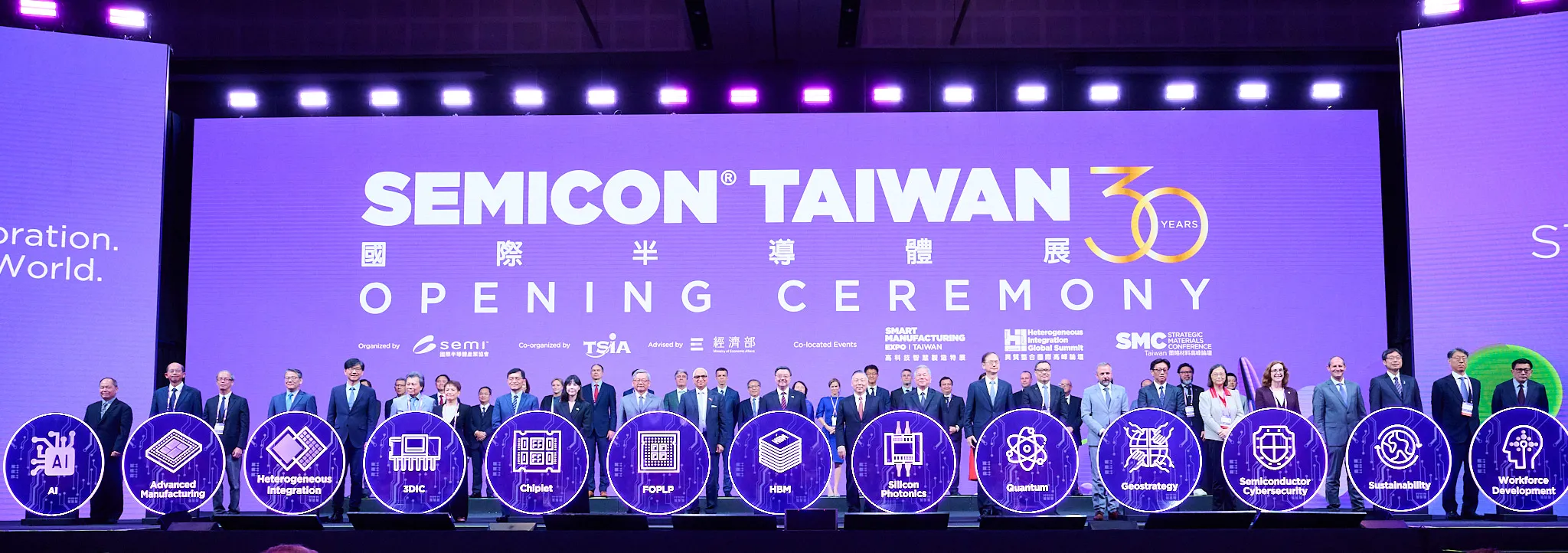
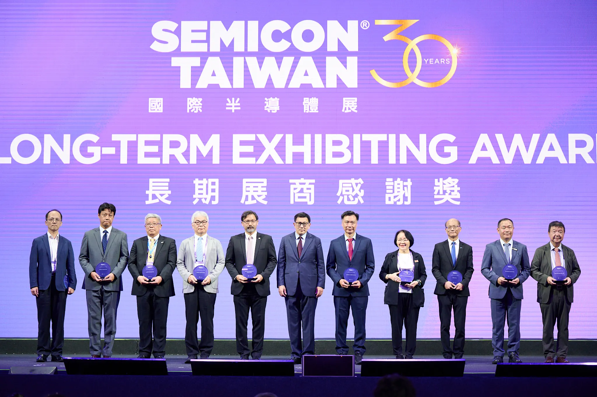
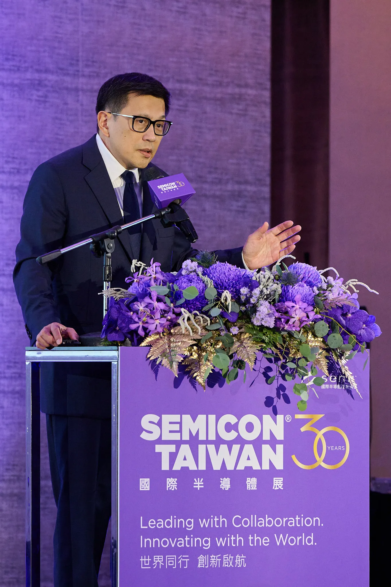
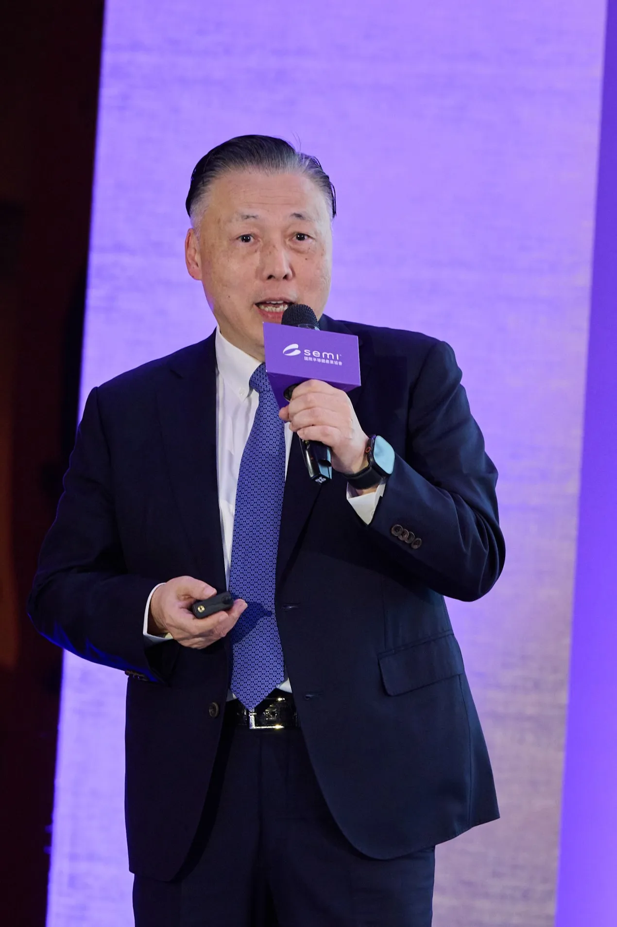
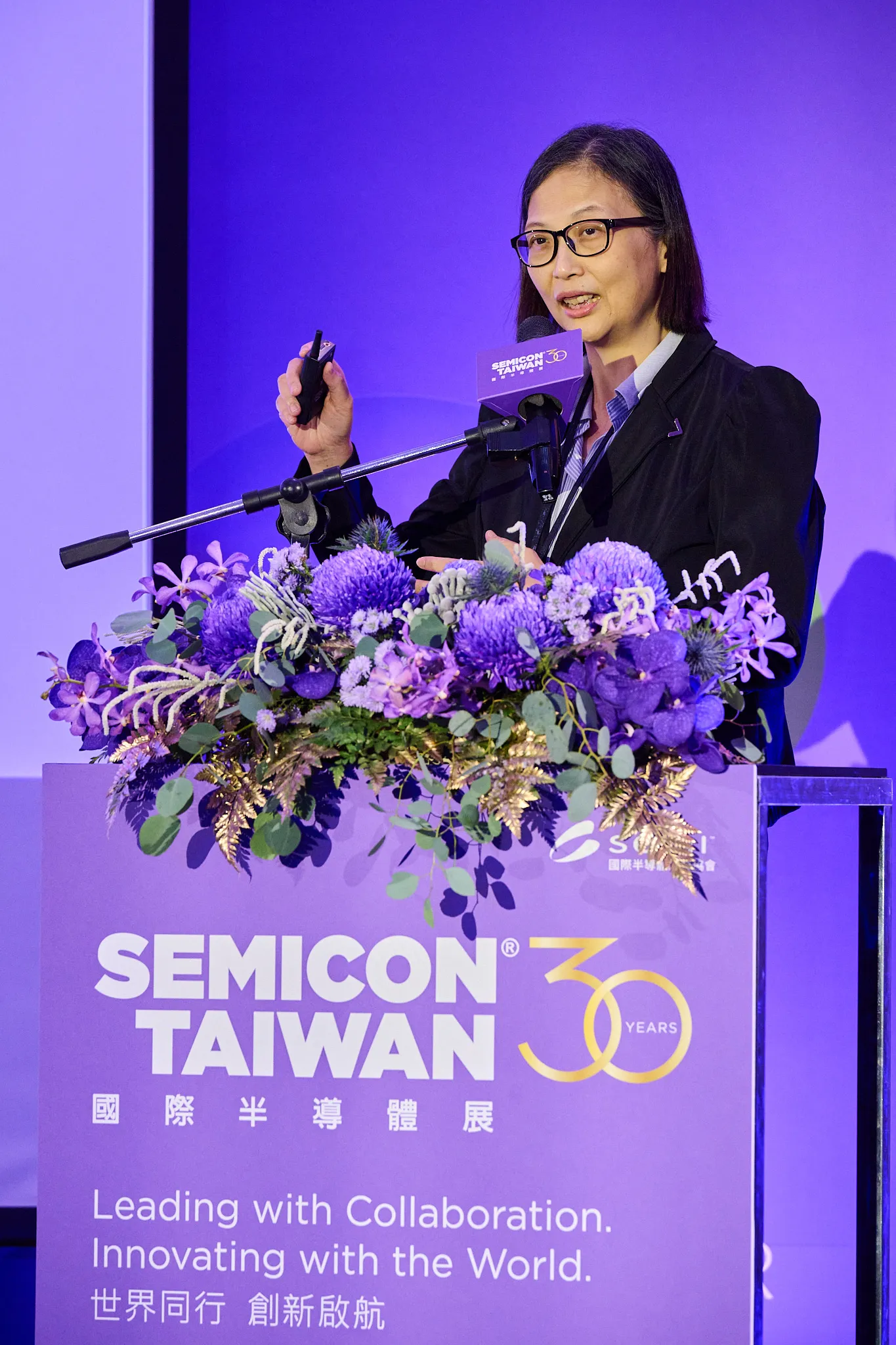
【Sept. 11th, 2025 – Hsinchu】SEMICON Taiwan 2025 opened yesterday at the Taipei Nangang Exhibition Center, celebrating its 30th anniversary with its largest-ever scale under the theme “Leading with Collaboration. Innovating with the World.” Premier Cho Jung-tai, SEMI President and CEO Ajit Manocha, and other industry leaders marked the opening with keynote remarks, followed by a recognition ceremony led by Terry Tsao, Global Chief Marketing Officer and President of Taiwan, SEMI, honoring long-term exhibitors.


▲Premier Cho Jung-tai, SEMI President and CEO Ajit Manocha, and industry leaders gather at SEMICON Taiwan 2025 opening ceremony, celebrating the exhibition's 30th anniversary milestone


Industry and Government Leaders Mark SEMICON Taiwan’s 30-Year Milestone

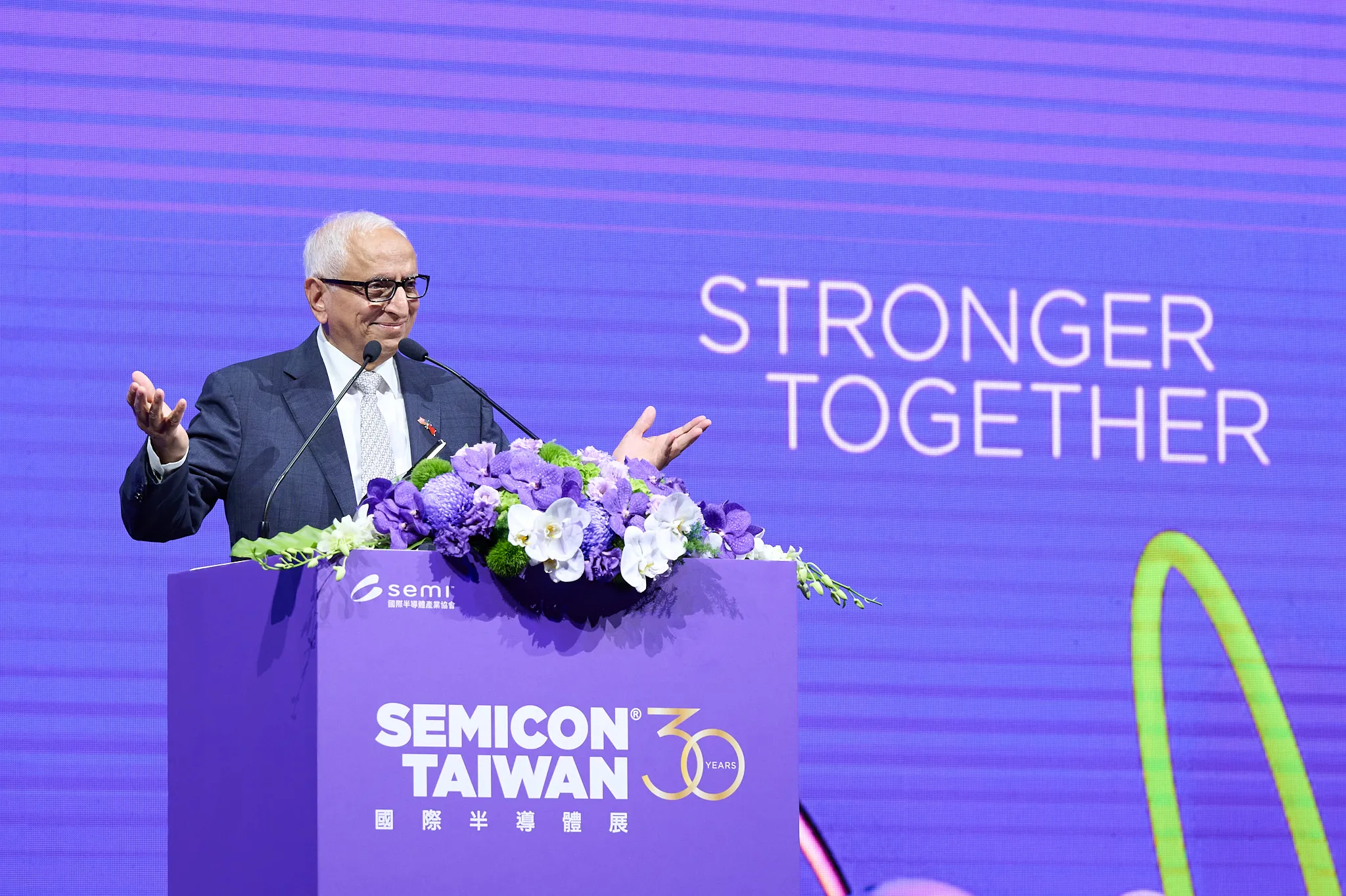
Manocha highlighted SEMICON Taiwan’s evolution over the past 30 years into a globally recognized platform at the heart of the semiconductor ecosystem. He noted that AI and quantum computing are ushering in a new chapter for the industry, and stressed that despite geopolitical challenges, semiconductors serve as “the foundation of humanity” and must continue to advance without pause.


▲SEMI President and CEO Ajit Manocha delivers keynote remarks, highlighting Taiwan's position at the heart of the global semiconductor ecosystem as AI and quantum computing drive industry transformation


Premier Cho welcomed global industry leaders to Taiwan, announcing over NT$30 billion in new investment for the “AI Ten Major Infrastructure” initiative covering silicon photonics, quantum computing, drones, and robotics. He noted Taiwan’s semiconductor output has reached NT$5.3 trillion and is on track to exceed NT$6 trillion, underscoring its commitment to supply chain resilience, global collaboration, and advancing technology in the AI era.

SC Chien, Executive Board Director of the Taiwan Semiconductor Industry Association (TSIA) and President of UMC, highlighted the rising importance of semiconductors in today’s fast-changing landscape. He noted that Taiwan’s full value chain generated US$165.6 billion in 2024, underscoring its critical role in the global supply chain. Taiwan’s commitment to innovation and collaboration, he added, continues to propel the industry forward, with SEMICON Taiwan both celebrating technology and affirming a shared vision for the future.


Global Forums Spotlight Innovation and Sustainability

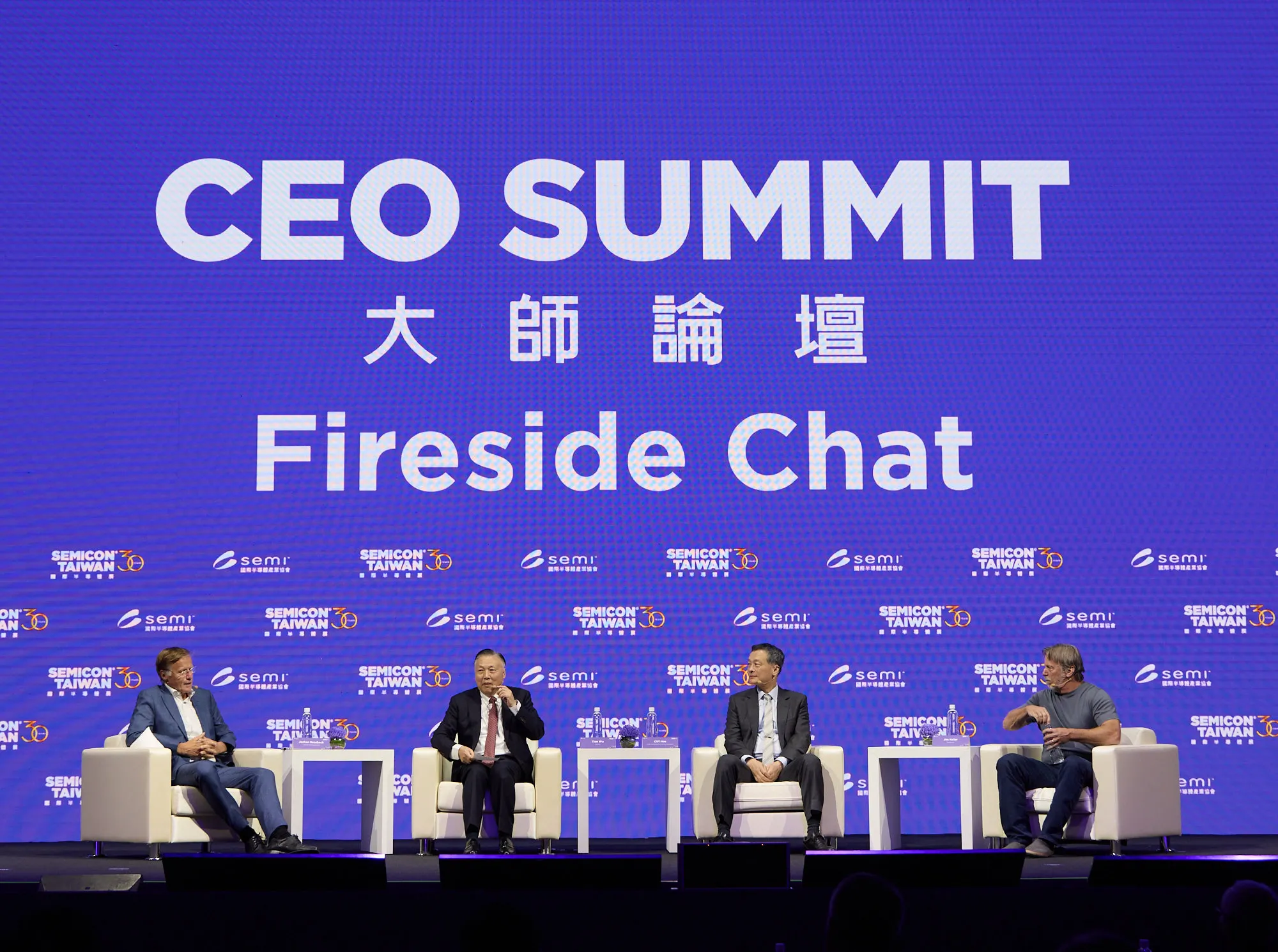
SEMICON Taiwan 2025 hosts over 25 international forums on technology, strategy, and sustainability. The CEO Summit drew strong attention, highlighted by the fireside chat “Navigating What’s Next: Global Opportunities and Taiwan’s Strategic Role” with Dr. Tien Wu, CEO of ASE and Chair of the SEMI International Board Executive Committee, and Cliff Hou, Chairman of  TSIA, Jochen Hanebeck, Infineon CEO, and Silicon Valley “chip legend” Jim Keller, delivering rare insights into AI innovation, global collaboration, and Taiwan’s place in the semiconductor landscape.


▲Terry Tsao, SEMI Global Chief Marketing Officer and President of Taiwan, presents recognition awards to long-term exhibitors, honoring their sustained support for SEMICON Taiwan


▲CEO Summit fireside chat featuring Dr. Tien Wu, CEO of ASE, and Cliff Hou, Chairman of TSIA, alongside Infineon and Tenstorrent CEOs exploring Taiwan's strategic role in the global semiconductor landscape


SEMI and TSIA co-hosted the Semiconductor Sustainability Summit, which explored net-zero pathways, AI-driven carbon reduction, and circular economy solutions, with keynotes from leaders including Dr. Arthur Chuang, Vice President of TSMC. The Summit introduced the SEMI Energy Collaborative and its efforts to advance decarbonization across Asia-Pacific, while the SEMI Forest exhibition highlighted global tree-planting and habitat restoration efforts, showcasing the industry’s tangible commitment to sustainability.

SEMICON Taiwan 2025 is underway through September 12, hosting industry professionals to experience the latest innovations and global exchange. For more information on SEMICON Taiwan 2025, visit the offical Website.
 

About SEMI

SEMI® is the global industry association connecting over 3,000 member companies and 1.5 million professionals worldwide across the semiconductor and electronics design and manufacturing supply chain. We accelerate member collaboration on solutions to top industry challenges through Advocacy, Workforce Development, Sustainability, Supply Chain Management, and other programs. Our SEMICON® expositions and events, technology communities, standards, and market intelligence help advance our members’ business growth and innovations in design, devices, equipment, materials, services, and software, enabling smarter, faster, more secure electronics. Visit  www.semi.org or join SEMI Facebook, and SEMI LinkedIn, and SEMI Official Line Account.


Lam Research Introduces VECTOR® TEOS 3D to Address Critical Advanced Packaging Challenges in Chipmaking 

Inter-Die Gapfill Tool Expands Industry-Leading Portfolio of Solutions for 3D Integration and Chiplet Technologies; Paves Way for New, AI-Accelerating Architectures 

FREMONT, Calif., Sept. 9, 2025 -- Lam Research Corp. (Nasdaq: LRCX) today unveiled VECTOR® TEOS 3D, a breakthrough deposition tool engineered specifically for the advanced packaging of next-generation chips required for artificial intelligence (AI) and high-performance computing (HPC) applications. TEOS 3D is purpose-built to solve critical challenges in 3D stacking and high-density heterogeneous integration. It provides ultra-thick, uniform, inter-die gapfill, leveraging a proprietary bowed wafer handling approach, innovations in dielectric deposition, and enhanced monitoring by Lam Equipment Intelligence® technology. TEOS 3D is installed at leading logic and memory fabs around the world. 

"VECTOR TEOS 3D deposits the industry's thickest, void-free, inter-die gapfill films, customized to meet the challenging requirements of advanced die stacking integration schemes, even on ultra-stressed, high-bow wafers," said Sesha Varadarajan, senior vice president of the Global Products Group at Lam Research. "It's another powerful addition to our best-in-class advanced packaging portfolio, which delivers the differentiated, atomic-level innovations chipmakers need to scale beyond Moore's Law and into the AI era."

Addresses Manufacturing Pain Points

The explosive growth of AI is driving the need for new devices that can support increasingly data-intensive workloads. Chipmakers are turning to 3D advanced packaging to integrate multiple dies into chiplet architectures to enable AI compute. By bringing memory and processing closer together to optimize electrical pathways, chiplet designs can improve processing speed, and pack more power into smaller form factors. However, as chiplets scale taller and become more complex, they present a range of new manufacturing hurdles, from stress during processing that can distort or bow a wafer's shape, to cracks and voids in films that cause defects and lower yield. 

TEOS 3D conquers a range of critical advanced packaging production challenges, excelling at handling bulky, high-bow wafers precisely and reliably. With nanoscale precision, it deposits specialized dielectric films of up to 60 microns thick between dies, with scalability to deposit films greater than 100 microns. The films provide essential structural, thermal and mechanical support to prevent common packaging failures such as delamination. TEOS 3D also features Lam's novel clamping technology and an optimal pedestal design that provides exceptional stability when processing thick wafers, enabling uniform film deposition even when dealing with extreme wafer bow. 

Other highlights include: 

  • The first solution for single-pass processing of crack-free films more than 30 microns thick, significantly enhancing yield and process time.
  • Unique quad station module (QSM) architecture to boost productivity: Lam's proven QSM architecture features four distinct stations to enable parallel processing and reduce bottlenecks. The modular design helps deliver nearly 70%1 faster throughput and up to 20% improvement in cost of ownership compared to Lam's previous generation of gapfill solutions.
  • Lam Equipment Intelligence® technology for process repeatability: Built into TEOS 3D, Equipment Intelligence solutions boost equipment performance and reliability, and drive yield improvement by using smart technology to monitor processes, fix issues faster, and automate routine tasks.
  • Enhanced energy efficiency: Integrated high-efficiency RF generators and ECO Mode peripheral control reduce energy consumption while improving process precision. 

Joins an Industry-Leading Suite of Advanced Packaging Solutions 

Leveraging the company's 15 years of leadership in advanced packaging and decades of expertise in dielectric films, TEOS 3D builds on Lam's existing VECTOR® Core and TEOS product families, representing continuous innovation in materials and processes for integrated packaging. It is part of a comprehensive product portfolio of industry-leading solutions that addresses critical challenges and drives innovation and productivity across the advanced packaging workflow. 

Media Resources 

About Lam Research 

Lam Research Corporation is a global supplier of innovative wafer fabrication equipment and services to the semiconductor industry. Lam's equipment and services allow customers to build smaller and better performing devices. In fact, today, nearly every advanced chip is built with Lam technology. We combine superior systems engineering, technology leadership, and a strong values-based culture, with an unwavering commitment to our customers. Lam Research (Nasdaq: LRCX) is a FORTUNE 500® company headquartered in Fremont, Calif., with operations around the globe. Learn more at www.lamresearch.com

1 – Based on internal testing; 68%. 

Caution Regarding Forward-Looking Statements 

Statements made in this press release that are not of historical fact are forward-looking statements and are subject to the safe harbor provisions of the Private Securities Litigation Reform Act of 1995. Such forward-looking statements relate to, but are not limited to: industry trends, demands, expectations and requirements; the requirements of our customers; and the capabilities and performance of our products. Some factors that may affect these forward-looking statements include: business, economic, political and/or regulatory conditions in the consumer electronics industry, the semiconductor industry and the overall economy may deteriorate or change; the actions of our customers and competitors may be inconsistent with our expectations; trade regulations, export controls, tariffs, trade disputes, and other geopolitical tensions may inhibit our ability to sell our products; supply chain cost increases, tariffs and other inflationary pressures have impacted and may continue to impact our profitability; supply chain disruptions or manufacturing capacity constraints may limit our ability to manufacture and sell our products; and natural and human-caused disasters, disease outbreaks, war, terrorism, political or governmental unrest or instability, or other events beyond our control may impact our operations and revenue in affected areas; as well as the other risks and uncertainties that are described in the documents filed or furnished by us with the Securities and Exchange Commission, including specifically the Risk Factors described in our annual report on Form 10-K for the fiscal year ended June 29, 2025. These uncertainties and changes could materially affect the forward-looking statements and cause actual results to vary from expectations in a material way. The Company undertakes no obligation to update the information or statements made in this press release. 

Company Contacts: 

Allison L. Parker 

Media Relations 

(510) 572-9324 

[email protected] 

Ram Ganesh 

Investor Relations 

(510) 572-1615 

[email protected] 

Source: Lam Research Corporation, (Nasdaq: LRCX)

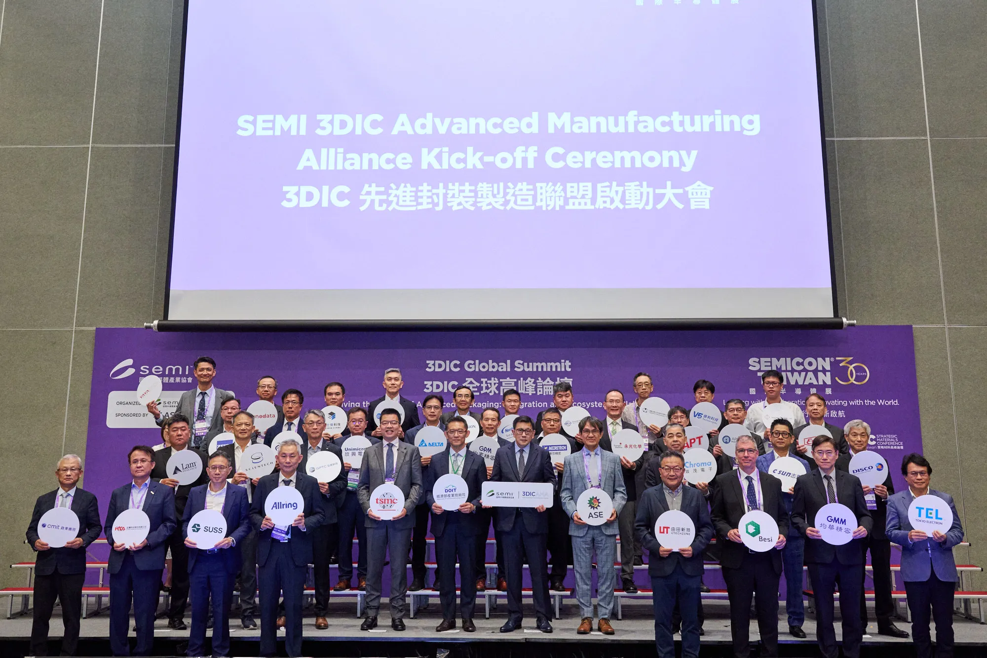
【Sept. 11th, 2025 – Hsinchu】With surging demand for generative AI, high performance computing (HPC), memory, and heterogeneous integration, the semiconductor industry is confronting the limits of traditional scaling. At SEMICON Taiwan 2025, SEMI announced the launch of the 3DIC Advanced Manufacturing Alliance (3DICAMA), co-chaired by TSMC and ASE and joined by 37 leading companies, including All Ring, Chroma, Delta, Everlight Chemical, GMM, Grand Process, Scientech, and Unimicron, to advance cross-disciplinary collaboration, standardization, and the complete 3DIC ecosystem.


▲3DICAMA launches to drive standards, innovation, and yield breakthroughs across the semiconductor ecosystem


AI Era Drives 3DIC Growth

According to Yole Intelligence, the advanced packaging market is expected to more than double from US$38B in 2024 to US$79B in 2030 (12.7% CAGR), fueled by AI and high bandwidth memory (HBM) advancements. Rising demand for high-performance, low-power, high-density solutions positions 3DIC as a critical integration technology, though challenges in heterogeneous integration, thermal management, and interconnects remain. With its strong semiconductor ecosystem, advanced manufacturing, and contributions to global standards, Taiwan is playing an increasingly important role in 3DIC and advanced packaging.


3DICAMA Launches to Drive Cross-Domain Collaboration and Ecosystem Growth

Co-chaired by Dr. Jun He, Vice President of Advanced Packaging Technology and Service at TSMC, and Dr. Mike Hung, Senior Vice President at ASE, 3DICAMA unites industry partners to strengthen supply chain collaboration, boost resilience, and establish technical standards across materials, processes, and design. The alliance will also advance 3DIC R&D to improve efficiency and yield, address thermal and interconnect challenges, and accelerate commercialization through enhanced testing, quality, software, and automation, building a complete and sustainable 3DIC ecosystem.


SEMI Unites Global Resources to Accelerate 3DIC Ecosystem

“3DICAMA highlights SEMI’s role in driving global collaboration,” said Terry Tsao, SEMI Global Chief Marketing Officer and President of Taiwan, SEMI. “By uniting global resources, fostering industry-policy dialogue, and accelerating commercialization, we aim to deliver faster, more efficient, and more competitive solutions for applications such as AI, HPC, and data centers.”

The launch ceremony underscored the industry’s commitment to innovation, with Dr. Chao-Chung Kuo, Director General of the Department of Industrial Technology, MOEA, highlighting the Alliance’s significance in advancing Taiwan’s packaging ecosystem and strengthening collaboration across industry, government, and academia.
 

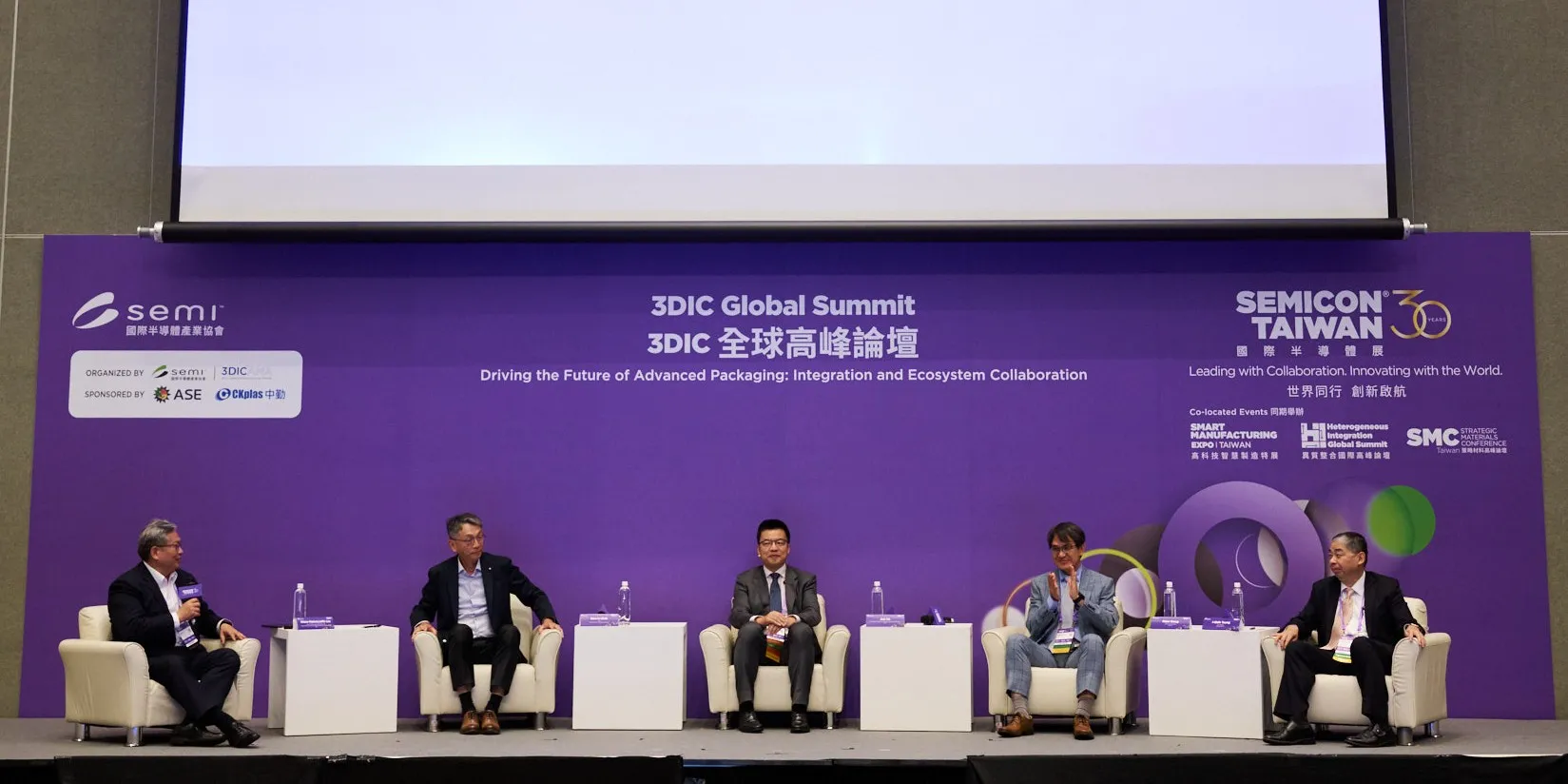
▲TSMC, ASE, Chroma ATE, and Grand Process leaders discuss technology roadmaps and applications


Global 3DIC Summit Charts the Future of Advanced Packaging

The Global 3DIC Summit, themed ”Driving the Future of Advanced Packaging: Integration and Ecosystem Collaboration,” featured a keynote by Vince Hu, Corporate Vice President of MediaTek, and a panel moderated by Dr. Chao-Hsien (Jeff) Lin of ITRI with industry leaders including Dr. Jun He of TSMC, Dr. Mike Hung of ASE, Dr. I-Shih Tseng of Chroma ATE, and Ben-Li Shih of Grand Process Technology. The discussions focused on AI-driven 3DIC challenges, supply chain resilience, and automation, underscoring Taiwan’s strategic role in the global advanced packaging ecosystem.

For more information on SEMICON Taiwan 2025, visit the offical Website.
 

About SEMI

SEMI® is the global industry association connecting over 3,000 member companies and 1.5 million professionals worldwide across the semiconductor and electronics design and manufacturing supply chain. We accelerate member collaboration on solutions to top industry challenges through Advocacy, Workforce Development, Sustainability, Supply Chain Management, and other programs. Our SEMICON® expositions and events, technology communities, standards, and market intelligence help advance our members’ business growth and innovations in design, devices, equipment, materials, services, and software, enabling smarter, faster, more secure electronics. Visit  www.semi.org or join SEMI Facebook, and SEMI LinkedIn, and SEMI Official Line Account.


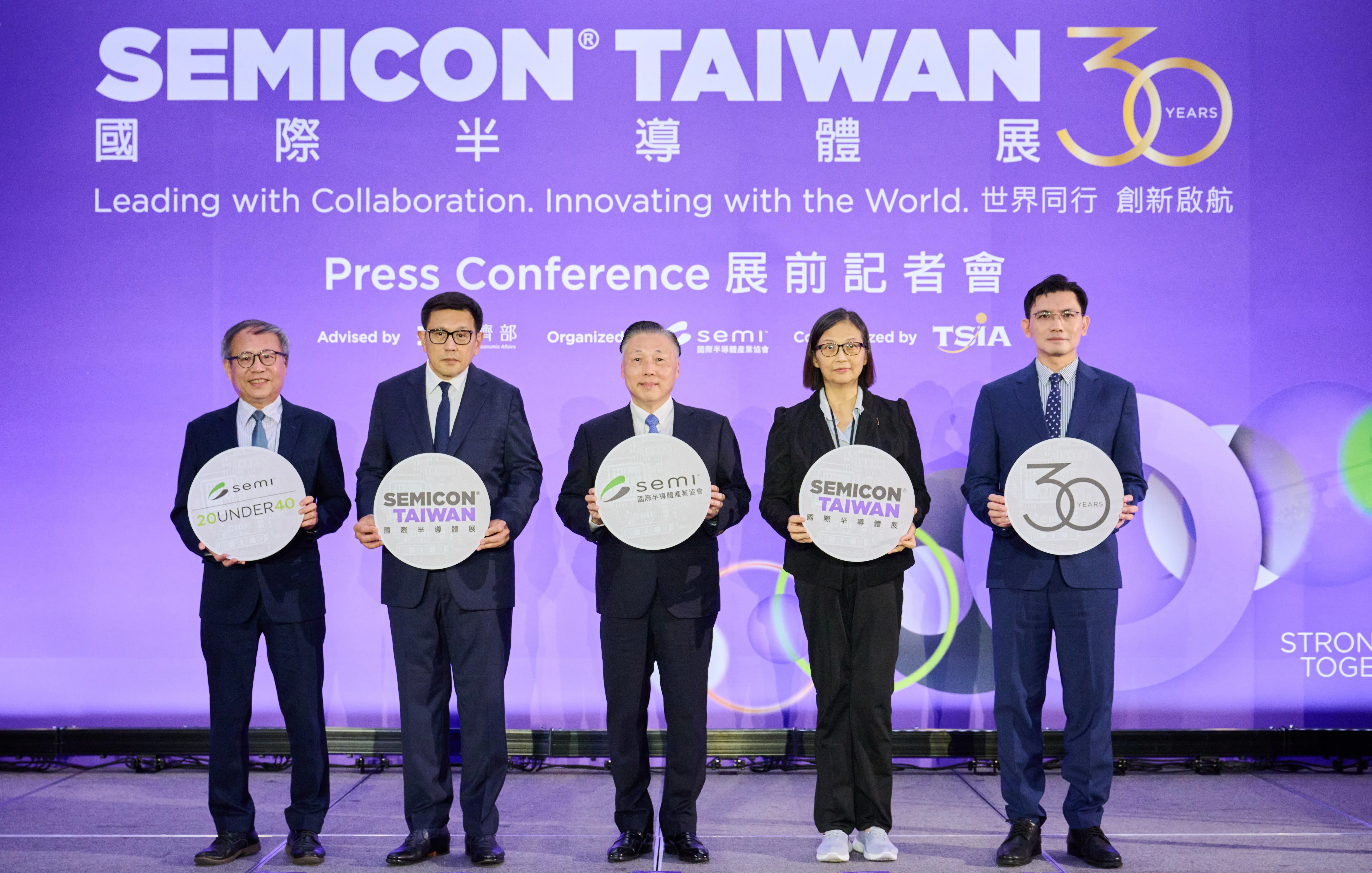
【Sept. 8th, 2025 – Hsinchu】SEMICON Taiwan 2025, the region’s most influential semiconductor event, opens this week. At today’s pre-show press conference, Terry Tsao, Global Chief Marketing Officer and President of Taiwan, SEMI; Dr. Tien Wu, Chair of the SEMI International Board Executive Committee and CEO of ASE; Doris Hsu, SEMI International Board of Director and Chairperson and CEO of GlobalWafers; Professor Tzi-Dar Chiueh, Dean of the College of Advanced Technology at National Taiwan University (NTU) and CEO of the Taiwan Chip-based Industrial Innovation Program Office; and Clark Tseng, Senior Director of Market Intelligence at SEMI, joined leaders from industry, government, and academia to share forward-looking perspectives on the semiconductor industry.


▲Joined leaders from industry, government, and academia at the SEMICON Taiwan 2025 pre-show press conference


The focal point of International Semiconductor Week, this year’s SEMICON Taiwan adopts the theme Leading with Collaboration. Innovating with the World. The event features 25+ forums and 13 key technology themes, highlighting collaboration as the catalyst for the next wave of innovation. Industry leaders will share insights on AI-driven semiconductor trends, market strategies, and reveal key industry data.


AI Wave Drives Global Semiconductor Growth with Record Equipment Investments

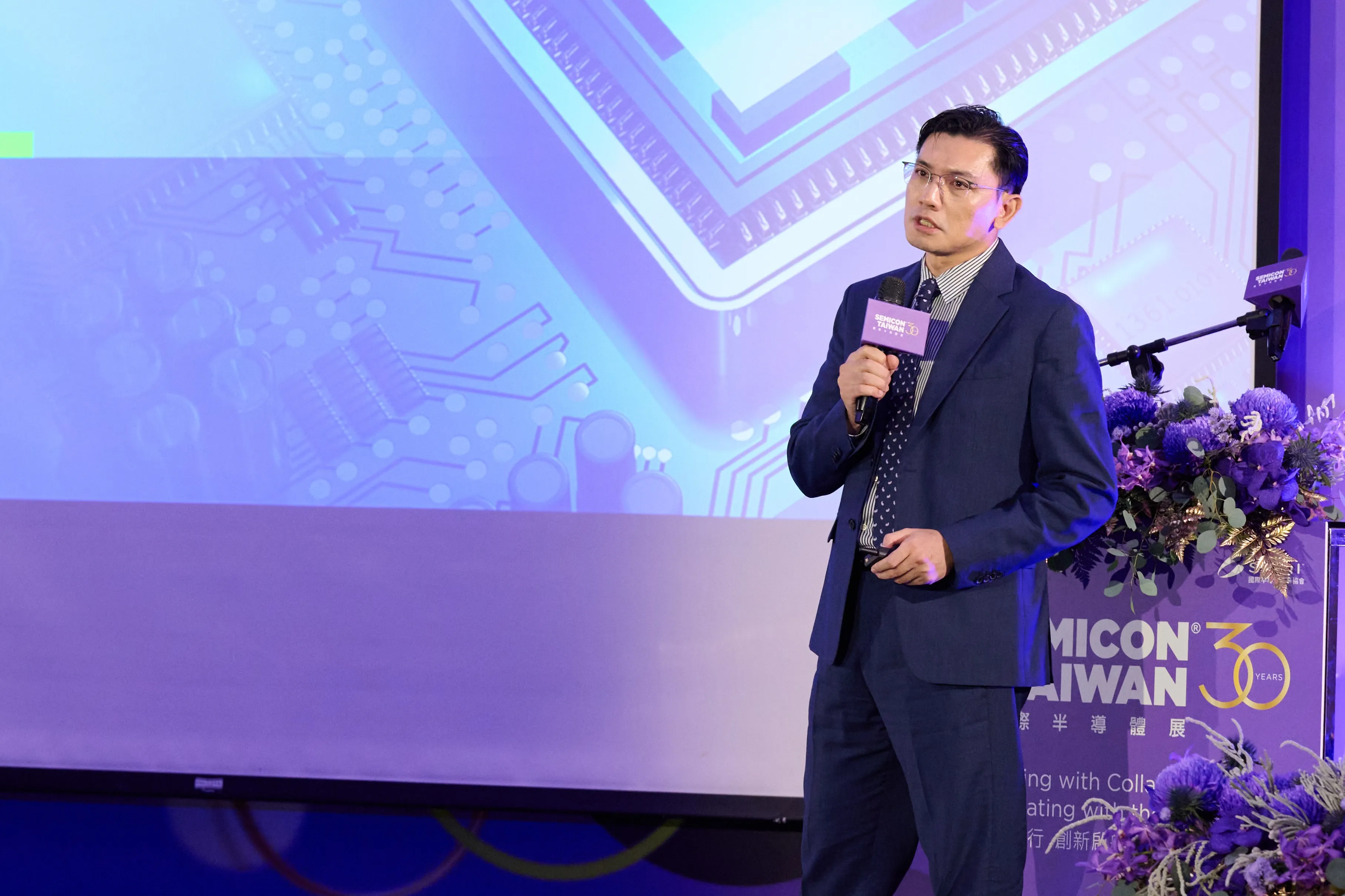
According to SEMI’s latest Market Intelligence, AI is extending from the cloud to the edge and end devices, driving demand not only in data centers but also for local real-time computing. Capital expenditures by the top four cloud service providers are projected to grow from US$210 billion in 2024 to US$310 billion in 2025, fueling the demand for AI infrastructure. In 2025, AI and high-performance computing (HPC) related equipment investments are expected to account for 40% of global semiconductor equipment spending, and this share is anticipated to exceed 55% by 2030.

The global semiconductor equipment market is forecast to grow by 7.4% to $125.5 billion in 2025, with a further increase of 10% to reach a new high in 2026. Taiwan's investments are projected to reach $28 billion in 2025, an increase of over 70% year-on-year, driven by strong investments in HPC and advanced packaging. In terms of AI/HPC and memory transformation, GAA, HBM, 3D stacking, and chiplet packaging are becoming the focus of investment. 


▲Clark Tseng, Senior Director of Market Intelligence at SEMI


SEMI Leads New Model of Global Industry Collaboration with Standards and Alliances

Amid rising semiconductor investment, the industry is shifting from supply chains to ecosystem collaboration. “SEMI connects the entire value chain, from design and manufacturing to packaging and system applications, helping members seize emerging opportunities,” said Terry Tsao. “The theme of ‘Leading with Collaboration. Innovating with the World.’ captures this shift, as SEMICON has become the unique global platform uniting the full value chain, with SEMICON Taiwan bringing the top industry players from around the world together to advance technology.”

Building on this vision, SEMI has advanced key standards and alliances. After launching the Silicon Photonics Alliance (SiPhIA) in 2024 with TSMC, ASE, and over 100 companies, SEMICON Taiwan 2025 will introduce the SEMI 3DIC Advanced Manufacturing Alliance (3DICAMA). The event will also mark the launch of certification for SEMI E187, the world’s first semiconductor equipment cybersecurity standard initiated by Taiwan, reinforcing Taiwan’s role in shaping the global semiconductor ecosystem.


▲Terry Tsao, Global Chief Marketing Officer and President of Taiwan, SEMI


Tech Strength and Supply Chain Resilience Drive Confidence

Seizing vast AI opportunities, the semiconductor industry is demonstrating strong investment confidence. Dr. Tien Wu, Chair of the SEMI International Board Executive Committee and CEO of ASE, said: “The semiconductor industry is projected to surpass US$1 trillion in the next decade, reshaping the global value chain. Taiwan must leverage its leadership in advanced manufacturing processes for AI and data center applications, as well as capitalize on the region's robust semiconductor ecosystem to strengthen its competitiveness through effective communication and a strategic focus on collaboration,”.

Doris Hsu, SEMI International Board of Directors and Chairperson and CEO of GlobalWafers, said, "AI is driving the strongest growth in both demand and pricing, and Taiwan’s complete ecosystem enables the industry to respond quickly to global needs while serving as a vital hub for supply chain collaboration."
 

▲Dr. Tien Wu, Chair of the SEMI International Board Executive Committee and CEO of ASE


▲Doris Hsu, SEMI International Board of Director and Chairperson and CEO of GlobalWafers


Chip-based Industrial Innovation Program Boosts Industry Alignment and Talent Growth

To reinforce industry investment, the government has introduced forward-looking policies through the Taiwan Chip-based Industrial Innovation Program. Professor Tzi-Dar Chiueh, Dean of the College of Advanced Technology at NTU and CEO of the Taiwan Chip-based Industrial Innovation Program Office, said: “Amid intense global competition, supply chain shifts, and rising innovation demands, the program is enabling Taiwan’s transition from manufacturing to innovation leadership and positioning the economy as a driving force in global semiconductor development.”

In response to the talent shortage, industry and academia are joining forces to cultivate the next generation, with early outcomes already visible. This year, the SEMI Taiwan 20 Under 40 Award honored 24 outstanding professionals under 40, reflecting progress in developing a strong talent pipeline. As part of the selection committee, Professor Chiueh noted that aligning policy direction with industry investment needs will provide a solid foundation for strengthening competitiveness in the AI era.


▲Professor Tzi-Dar Chiueh, CEO of the Taiwan Chip-based Industrial Innovation Program Office


Startup Zone Debuts, Driving Innovation and Ecosystem Collaboration


SEMICON Taiwan 2025 will feature over 200 global speakers, with forums covering heterogeneous integration, leadership insights from top CEOs, and the Memory Executive Summit bringing SK hynix, Samsung, and Micron together for the first time. A major highlight is the debut of the Silicon Startups Zone, co-organized with the IC Taiwan Grand Challenge (ICTGC), showcasing next-generation technologies such as 5G/6G, post-quantum cryptography, AI silicon photonics, SiC power devices, Wi-Fi 7 RF integration, and wireless charging. The zone will connect Taiwan’s complete supply chain to drive global investment, collaboration, and market growth, embodying the event theme: Leading with Collaboration. Innovating with the World.

“With its complete ecosystem spanning equipment, manufacturing, and applications, Taiwan is indispensable in the global supply chain,” said Tsao. “As AI reshapes the industry, Taiwan’s US$27.9 billion investment in semiconductor equipment underscores its central role, with SEMICON Taiwan serving as a vital platform for global collaboration and innovation.”

For more information on SEMICON Taiwan 2025 visit the offical Website.
 

About SEMI

SEMI® is the global industry association connecting over 3,000 member companies and 1.5 million professionals worldwide across the semiconductor and electronics design and manufacturing supply chain. We accelerate member collaboration on solutions to top industry challenges through Advocacy, Workforce Development, Sustainability, Supply Chain Management, and other programs. Our SEMICON® expositions and events, technology communities, standards, and market intelligence help advance our members’ business growth and innovations in design, devices, equipment, materials, services, and software, enabling smarter, faster, more secure electronics. Visit  www.semi.org or join SEMI Facebook, and SEMI LinkedIn, and SEMI Official Line Account.


【Sept. 3rd, 2025 – Hsinchu】SEMICON Taiwan 2025 enters its final countdown, spotlighting the global AI chip boom and the industry’s rapid transformation. Widely seen as the barometer of the global semiconductor industry, SEMICON Taiwan has hit a new pre-registration record this year. Celebrating its 30th anniversary by kicking off a full International Semiconductor Week, the event will gather 1,200+ companies, 4,100 booths, and industry partners from 56 countries. It opens with forums on September 8, followed by the exhibition at Taipei Nangang Exhibition Center, September 10-12.


Advanced Process Capacity Surges as Global Demand Accelerates

Soaring AI demand is fueling rapid semiconductor growth, with SEMI projecting sub-7nm capacity to reach a record 1.4 million wafers per month by 2028, a 69% jump from 2024. Leveraging robust ecosystems and resilient supply chains, the region continues to play a critical role in supporting global AI chip production. “The AI-driven growth wave is reshaping the industry,” said Terry Tsao, Global Chief Marketing Officer and President of Taiwan, SEMI. “As the industry shifts to cross-domain collaboration, leading system companies are forging closer partnerships across the semiconductor value chain.”
 

▲Advanced Process Capacity to Grow 70% by 2028, Fueling Cross-Domain Collaboration


Record International Participation Positions SEMICON Taiwan 2025 as a Global Hub

Fueled by Taiwan’s strength in AI semiconductors and its comprehensive ecosystem, SEMICON Taiwan 2025 will feature a record-high 17 national pavilions, including first-time participants from Canada, Costa Rica, Lithuania, Sweden, and Vietnam. Beyond record country pavilion participation, international delegations from the U.S., Chile, Spain, Italy, and more are visiting independently, underscoring the exhibition’s global appeal and growing role in industry collaboration.


▲SEMICON Taiwan 2025 Feature a Record 17 National Pavilions, Highlighting Global Appeal and Industry Collaboration


SEMICON Taiwan Leads Industry Dialogue and Fosters Innovation

SEMICON Taiwan 2025 will serve as a global platform with high-profile forums and specialized zones addressing AI-driven breakthroughs and supply chain resilience. On September 9, the IC Forum-Advanced Chip Technology and Manufacturing will feature TSMC, ASML, and Applied Materials, while the Semiconductor Cybersecurity Global Summit on September 12 will mark the official launch of SEMI E187 Certification. SEMI E187 is the world’s first semiconductor equipment cybersecurity standard led by Taiwan. By establishing a trusted certification system, it allows suppliers to demonstrate compliance, strengthens the entire supply chain, and empowers fabs to confidently integrate safer equipment, minimizing their exposure to cyber risks. With participating leaders including Foxconn and ITRI, discussions will focus on proactive strategies to safeguard the AI-era semiconductor supply chain. 

The AI Technology Zone will present the full value chain, from chip manufacturing and IC design to specialized hardware, featuring leaders such as Advantech, ASE, ASM, Aspeed, Egis Technology, and Zhen Ding. Addressing the need for a secure and reliable supply chain, the Semiconductor Cybersecurity Pavilion will showcase solutions in industrial control security and zero-trust architecture, providing comprehensive support for the AI era.

With SEMICON Taiwan 2025 less than a week away, there is limited time to get free registration. Register early to skip the line. For more details, visit the offical Website.
 

About SEMI

SEMI® is the global industry association connecting over 3,000 member companies and 1.5 million professionals worldwide across the semiconductor and electronics design and manufacturing supply chain. We accelerate member collaboration on solutions to top industry challenges through Advocacy, Workforce Development, Sustainability, Supply Chain Management, and other programs. Our SEMICON® expositions and events, technology communities, standards, and market intelligence help advance our members’ business growth and innovations in design, devices, equipment, materials, services, and software, enabling smarter, faster, more secure electronics. Visit  www.semi.org or join SEMI Facebook, and SEMI LinkedIn, and SEMI Official Line Account.


【Aug 28th, 2025 – Hsinchu】 SEMICON Taiwan 2025 is just two weeks away, and this year’s forums will welcome an extraordinary lineup of speakers. Silicon Valley “chip legend” Jim Keller will take the stage at the CEO Summit, while Dr. Chin-Tay Shih, a pioneering force in Taiwan’s semiconductor development, is confirmed to join the SEMI 20 Under 40 Awards Ceremony and Tech Master Forum. As the industry builds its central role in the AI era, global leaders will gather in Taipei to chart the future of semiconductor innovation.


▲SEMICON Taiwan Featuring Chip Guru Jim Keller and Industry Pioneer Dr. Chih-Tay Shih


Industry Legends Gather in Taiwan to Spotlight Innovation and Leadership

Tenstorrent CEO Jim Keller, renowned for his groundbreaking chip designs at Intel, Tesla, and AMD, will headline the CEO Summit with a keynote addressing the key technologies shaping the future of computing. A fireside chat focused on Taiwan’s strategic role in the global semiconductor landscape will follow, featuring co-moderators Dr. Tien Wu, CEO of ASE and Chair of the SEMI International Board Executive Committee, and Cliff Hou, Chairman of TSIA, along with panelists Jim Keller and Jochen Hanebeck, CEO of Infineon.

Also taking the stage, Dr. Chin-Tay Shih, a pioneering architect of Taiwan’s semiconductor rise, will reflect on his journey from ITRI to helping establish UMC, TSMC, and VIS, underscoring how Taiwan built a complete supply chain and laid the foundation for today’s AI era. Joining the Tech Masters Forum are Professor Y-W Peter Hong of NSTC, GC Hung, Senior VP of UMC, and Emily Hong, Chair and Chief Strategy Officer of Wiwynn Corporation.


Post-Moore Era: Heterogeneous Integration and Advanced Packaging Take Center Stage

With scaling reaching its limits, heterogeneous integration and advanced packaging have become the new frontier of innovation. SEMICON Taiwan will debut a dedicated Heterogeneous Integration Zone with nearly 60 companies. The zone includes the 3DIC Advanced Packaging Pavilion, Semiconductor Packaging Pavilion, and FOPLP Pavilion.

On September 9, the 3DIC Global Summit will bring together leaders from ASE, Chroma, GPTC, MediaTek and TSMC, to tackle key issues including efficiency, yield, cross-domain collaboration, and standardization. The day will also see the launch of the SEMI 3DIC Advanced Manufacturing Alliance (3DICAMA), rallying global industry leaders to drive collective innovation and propel advanced packaging into its next wave of breakthroughs.


Register now for SEMICON Taiwan 2025 to skip the lines. Industry professionals can get a free admission code by August 31. For more details visit the offical Website.


About SEMI

SEMI® is the global industry association connecting over 3,000 member companies and 1.5 million professionals worldwide across the semiconductor and electronics design and manufacturing supply chain. We accelerate member collaboration on solutions to top industry challenges through Advocacy, Workforce Development, Sustainability, Supply Chain Management, and other programs. Our SEMICON® expositions and events, technology communities, standards, and market intelligence help advance our members’ business growth and innovations in design, devices, equipment, materials, services, and software, enabling smarter, faster, more secure electronics. Visit  www.semi.org or join SEMI Facebook, and SEMI LinkedIn, and SEMI Official Line Account.
 

Belgium France Germany India Ireland Italy Japan Malaysia Russia Singapore South Korea Taiwan United States Vietnam Webinar_2025-SCM_360x317_Event_Calendar_SCM_2025 Business Executive Technical
Highlighted content

Join us for an insightful webinar as we present the findings from the 2025 Semiconductor Supply Chain Survey, a collaborative effort between the SEMI Supply Chain Management initiative and McKinsey & Company.

The annual survey aims to establish benchmarks for operational agility metrics, covering the entire value chain from material suppliers to OEMs, offering a comprehensive view of the landscape. New this year are additional insights on trends in LTAs and organizational supply chain management capabilities

During this webinar, we will share results from the survey uncovering key trends, challenges, and opportunities within the semiconductor supply chain. By attending, you'll gain valuable insights to benchmark your organization against peers, identify areas for improvement, and course-correct more effectively. Please contact us if you like to learn about how your company can participate in the SCM initiative.

United States

SCM

Join us for a webinar highlighting the 2025 Semiconductor Supply Chain Survey results, conducted by SEMI SCM initiative and McKinsey & Company. Gain fresh insights into operational agility, LTAs, and SCM capabilities across the value chain. Discover key trends, challenges, and opportunities to benchmark your organization and strengthen supply chain resilience.

Choose your session:

9:00 am - 10:00 am Off Add to Calendar 2025-09-23 09:00:00 2025-09-23 10:00:00 2025 Semiconductor Supply Chain survey: Insights for strategy and capabilities Join us for a webinar highlighting the 2025 Semiconductor Supply Chain Survey results, conducted by SEMI SCM initiative and McKinsey & Company. Gain fresh insights into operational agility, LTAs, and SCM capabilities across the value chain. Discover key trends, challenges, and opportunities to benchmark your organization and strengthen supply chain resilience.Choose your session:US/EU: 9:00 AM – 10:00 AM PT [ Register Now ]Asia/US: 5:00 PM – 6:00 PM PT [ Register Now ] United States SEMI.org [email protected] America/Los_Angeles public America/Los_Angeles

Speakers


Henry Marcil

Partner

McKinsey & Company

Bio: Leader in McKinsey’s Advanced Industries Practice, focused on semiconductors n and key end markets (e.g., high tech)

Leads McKinsey’s Resiliency and Geopolitics service line in Semiconductor


Kushal Jolapara

Engagement Manager

McKinsey & Company

Bio: Manager in McKinsey's Operations practice, with a focus on product development and procurement service lines

Leads Supply Chain studies for Advanced Industries clients including Aerospace, Auto and Semiconductors

Dan Peacock

Engagement Manager

McKinsey & Company

Bio: Manager in McKinsey’s Operations Practice, focused on procurement and capital projects

Leads Operations projects at Foundries, IDMs, and equipment clients


Event Contact:

Krish Dharma

[email protected]

Agenda

•    Lead times throughout the semiconductor value chain
•    Landscape and trends in purchasing agreements and LTAs
•    Demand forecasts, backlogs, and end markets
•    Market outlook, opportunities, and threats
•    New for 2025: Organizational capabilities in supply chain management

Event format
Tab Order
Overview
New Tab 2
New Tab 1
Registration
Promote in calendar
Off