Registration is Now Open
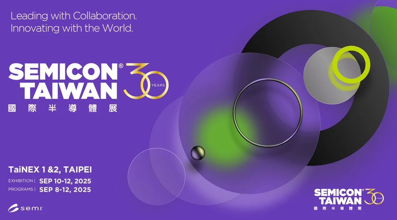
【June 18, 2025 – Hsinchu】SEMI today officially announced the launch of SEMICON Taiwan 2025, the annual premier event for the global semiconductor industry. Marking its 30th anniversary, the exhibition spotlights Taiwan’s rise as a collaborative innovation powerhouse. This year’s edition kicks off with a series of summit forums starting September 8, with the main exhibition officially opening from September 10 - 12 at Taipei Nangang Exhibition Center. Under the theme Leading with Collaboration. Innovating with the World, SEMICON Taiwan will strengthen global ecosystem partnerships and power the next wave of industry innovation.
Growth Amid Challenges: Open Collaboration Defines the New Industry Paradigm
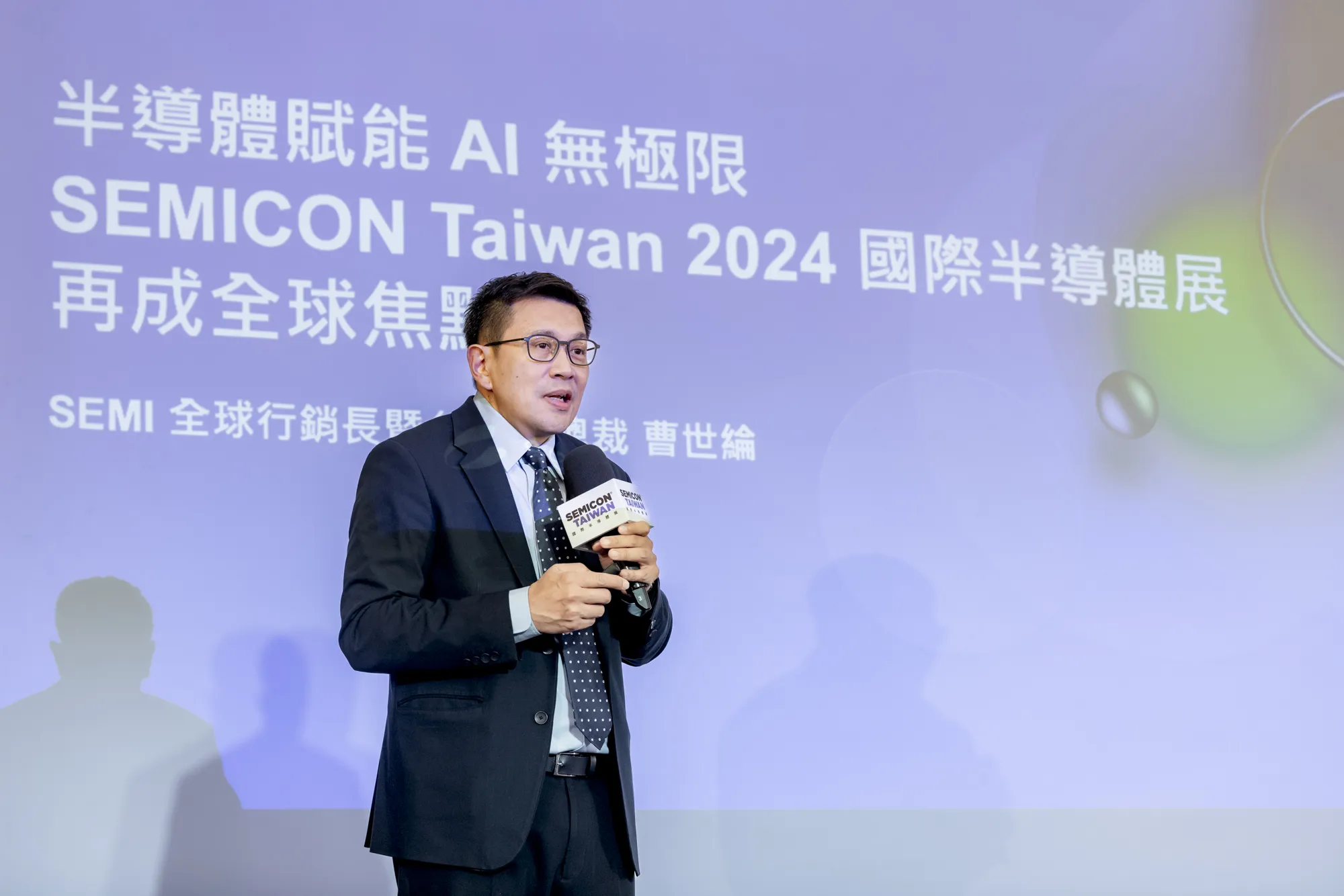
“Global semiconductor equipment shipments hit US$32.05 billion in Q1 2025, up 21% YoY, driven by strong demand for AI, cloud, HPC, and edge applications*,” said Terry Tsao, Global Chief Marketing Officer and President of Taiwan, SEMI. “Even with this robust growth, supply chain and geopolitical challenges remain. As a crucial global semiconductor hub, Taiwan is fully committed to pushing forward with new technologies and standards. Our theme, Leading with Collaboration. Innovating with the World. reflects our drive to foster innovation and strengthen global partnerships. SEMI will continue to work with partners to build a resilient and highly connected ecosystem.”
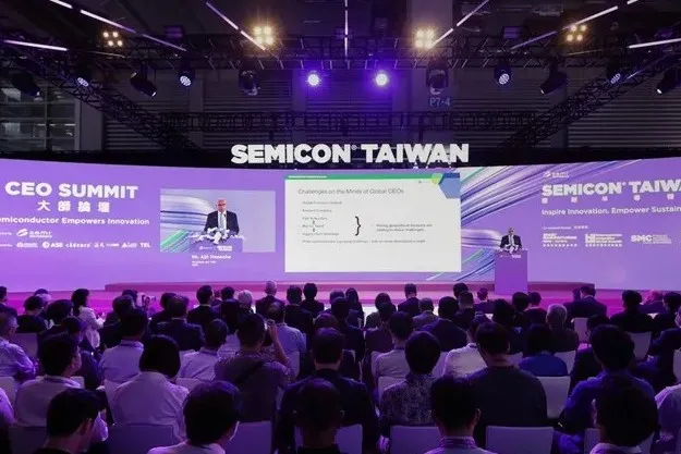
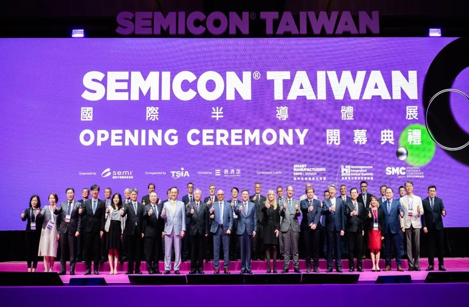
▲SEMICON Taiwan 2025 Marks Official Launch
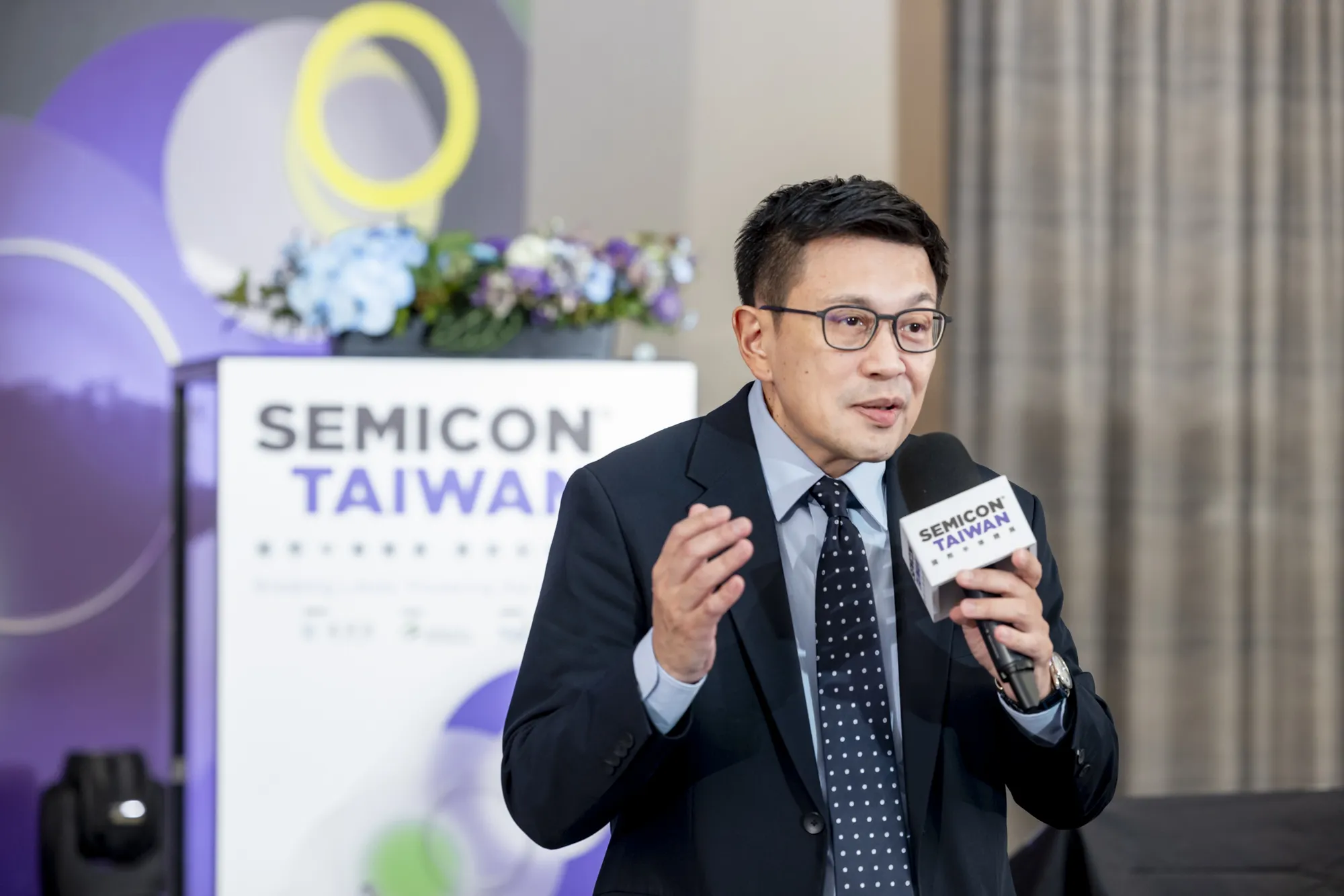
▲Terry Tsao, Global Chief Marketing Officer and President of Taiwan, SEMI
Highlights of SEMICON Taiwan 2025
● Significant Scale-Up Aims to Bolster Global Semiconductor Ecosystem Ties: SEMICON Taiwan 2025 is set to break records, bringing together over 1,100 companies and industry partners from 56 countries, with more than 100,000 visitors expected to explore the latest semiconductor trends. For the first time, the event expands into a full International Semiconductor Week, featuring global forums on September 8 – 9 to deepen technical exchange and cross-border collaboration. A record 17 Country Pavilions further highlight Taiwan’s crucial role in the global semiconductor supply chain, providing an enhanced platform for industry dialogue and partnerships.
● Showcasing Cutting-edge Technologies and Delivering the World’s Most Comprehensive Semiconductor Insights: Fueled by soaring AI and HPC demand, the semiconductor industry is entering the ‘Hyper Moore’s Law’ era, advancing chip architectures beyond the nanometer scale into the angstrom era and driving greater system integration and miniaturization in packaging. As a leading innovation platform, SEMICON Taiwan 2025 will spotlight breakthroughs in advanced manufacturing and cutting-edge packaging technologies such as 3DIC, chiplets, and FOPLP. The event will also cover key innovations including silicon photonics, high-bandwidth memory (HBM), and backside power delivery networks (BSPDN), highlighting technologies that are reshaping the industry and defining the future of semiconductors.
As AI investment and cross-sector collaboration grow, the semiconductor ecosystem is moving toward integrated co-creation. SEMICON Taiwan gathers over 200 leading companies and experts in more than 20 forums, offering in-depth industry insights and driving technology into practice.
● Driving Future Competitiveness Through Geostrategy, Talent Development, Sustainability, and Cybersecurity: In response to global supply chain restructuring and geopolitical challenges, this year’s forum will debut Geostrategy as a new theme. International delegations at SEMICON Taiwan will engage in bilateral and multilateral dialogues with Taiwan’s government and industry leaders, while dedicated sessions on semiconductor geostrategy will focus on enhancing supply chain resilience and global collaboration.
As AI talent competition intensifies and net-zero goals advance, SEMICON Taiwan 2025 will bolster industry resilience for the long term. The Workforce Development Pavilion will launch the SEMI 20 UNDER 40 Awards and hands-on activities to inspire future talent, while the High-Tech Facility Pavilion and expanded Green Manufacturing Area will highlight sustainable technologies and ESG leadership.
As a global leader in advanced manufacturing, innovation, and cybersecurity, Taiwan sets industry benchmarks as SEMI advances security frameworks for a safer ecosystem. With a focus on talent, sustainability, and collaboration, SEMICON Taiwan powers the next 30 years of sustainable innovation.
Registration for SEMICON Taiwan 2025 opens on June 18. Industry professionals can apply for free visitor discount codes through August 31. Super early bird registration for the International Semiconductor Forum is also available now, offering an exclusive 30% discount for a limited time. For more details, visit the Official website.
*Source: SEMI Report, June 5, 2025
▲Main Theme of SEMICON Taiwan 2025_Leading with Collaboration. Innovating with the World
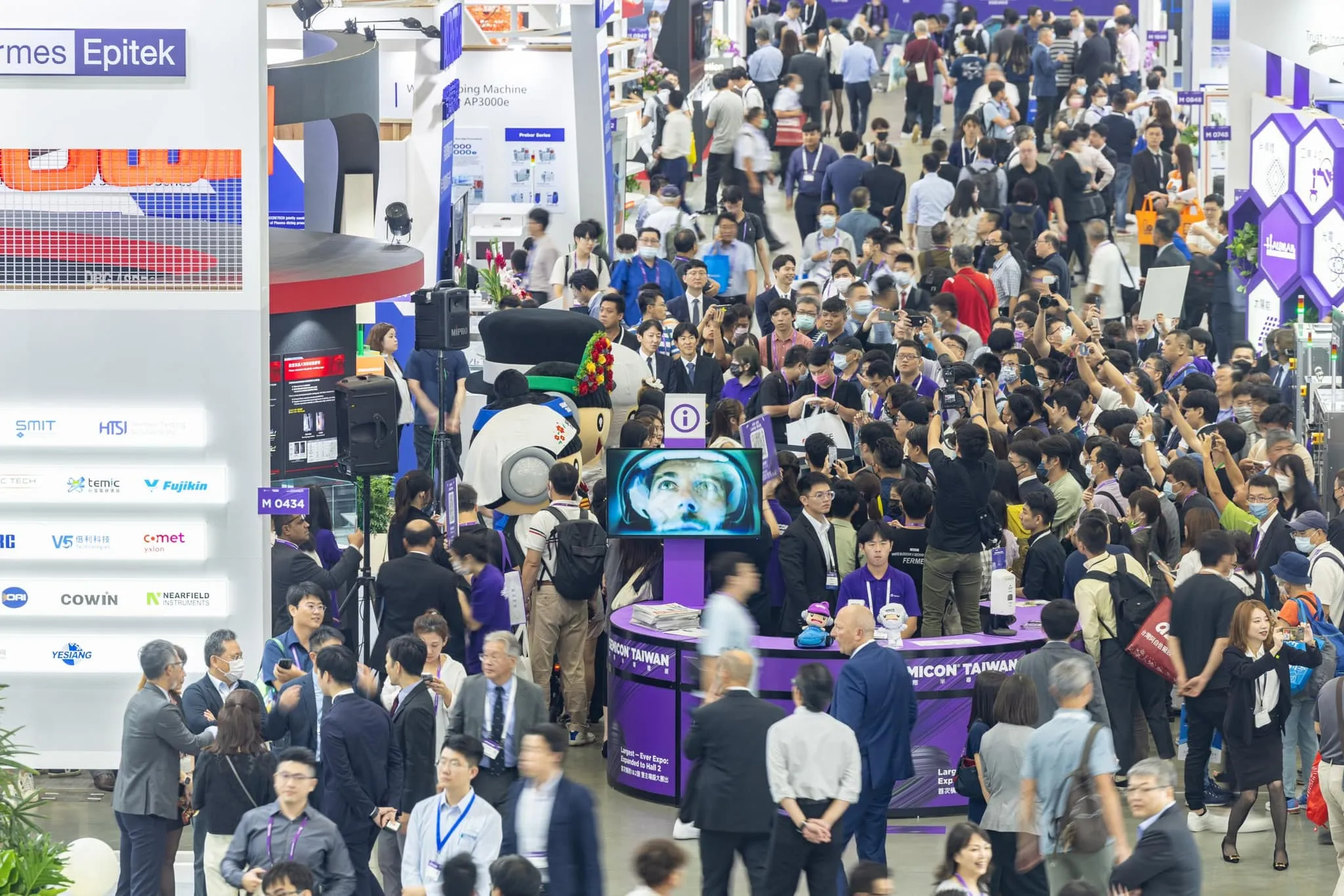
▲SEMICON Taiwan 2025 Is Set to Break Records With 100,000+ Visitors Expected
About SEMI
SEMI® is the global industry association for the semiconductor and electronics design and manufacturing supply chain, connecting over 3,000 member companies and 1.5 million professionals worldwide. Through diverse initiatives including policy advocacy, talent development, sustainability, and supply chain management, SEMI facilitates collaboration among members to address critical industry challenges. SEMI’s SEMICON® Taiwan exhibitions and events, technical communities, standardization, and market intelligence to empower members in driving business growth and innovation across design, devices, equipment, materials, services, and software, enabling smarter, faster, and more secure electronic technologies. For more information, visit www.semi.org or join SEMI Facebook, and SEMI LinkedIn.