REGISTRATION

- 사전등록 마감일: 2023년 5월 12일(금) 오후 3시
등록비용
- 사전등록 (5월 12일까지)
- SEMI 회원사: 28만원
- 비회원사: 33만원
- 현장등록
- SEMI 회원사: 33만원
- 비회원사: 38만원
※ 한 회사에서 5인 이상 등록할 경우 단체등록가가 적용됩니다. 단체등록은 이메일([email protected])로 문의 바랍니다.
OVERVIEW
- 날짜: 2023년 5월 17일(수)
- 시간: 09:00 - 17:30
- 장소: 수원컨벤션센터 컨벤션 2홀
SPONSORS
 |  |  |  |
 |  |  |  |
 |  |  |  |
![]()
NOTICE
- 아젠다는 연사 사정에 의하여 임의로 변경될 수 있습니다.
- 행사 종료 후 참석자들에게 연사 동의를 얻은 자료에 한하여 발표자료를 공유드릴 예정입니다.
CONTACT
- 프로그램팀 ([email protected])
대한민국
경기도 수원시
수원컨벤션센터 컨벤션 2홀
Welcome

Keynote
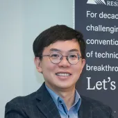
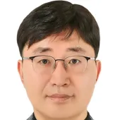
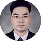
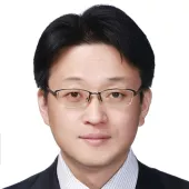
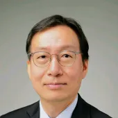
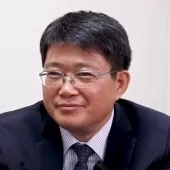
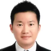
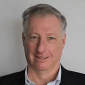
GAA(Gate-All-Around) technology to enable continuous CMOS transistor scaling for energy efficient computing solution
Namsung Kim is a Senior Director in the Integrated Module Solutions (IMS) Group at Applied Materials. He is currently responsible for managing customer engagement programs, driving business growth, and leading cross-functional teams (various Business Units) to deliver the integrated materials/modules-base product solutions across leading-edge CMOS Logic and Memory technologies. Prior to this role, he has successfully led & accomplished the definition of CMOS Logic technology roadmap, its inflections of future technology nodes and delivered multiple product development paths by validating innovative pathway solutions.
He joined Applied Materials, Inc., USA in 2015, bringing over 20 years of semiconductor device/process integration experiences (various engineering/management positions) from both CMOS Logic (GlobalFoundries/IBM alliance in USA and SSMC in Singapore) and Memory (SK-Hynix, previously LG Semi., in Korea) industries. He earned a MS in electrical and computer engineering from the National University of Singapore. He has authored and co-authored more than 50 technical publications and holds over 40 patents in the field of advanced logic (FinFETs and GAA devices) and memory technologies.
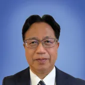
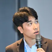
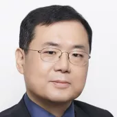
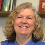
Market & Technology Trends for Memory Devices including Materials
Dr. Jeongdong Choe is a Senior Technical Fellow at TechInsights. He has over 30 years of experience in the semiconductor industry, R&D, and reverse engineering on DRAM, NAND/NOR FLASH, SRAM/Logic, and Emerging Memory. He worked for SK Hynix and Samsung Electronics for over 20 years. He joined TechInsights and has been focusing on technology analysis of semiconductor processes, materials, devices, and architecture. He has written many articles on memory technology including roadmaps, technology trends, and detailed comparisons.
Global Supply Chain
Break
Session 1: Advanced Materials for Enabling Next-Generation Devices
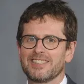
Precursors for Memory
Jean-Marc Girard Ph.D. is CTO and Sr. VP of Manufacturing Technologies at Air Liquide Advanced Materials (ALAM), and an Air Liquid Group Fellow. He has 25 years of experience of R&D and product development management in the field of semiconductor materials and process technology in Europe, Japan and the US, and is one of the founders and was the global director of ALOHA™ from 2005 to 2010 (Air Liquide’s original CVD/ALD materials product line).
Within ALAM, Jean-Marc globally manages the Research and Development for deposition & advanced dry etching materials, oversees strategic engagements and collaborations with leading customers and equipment companies, and supervises the Intellectual Property generation and portfolio management. Since 2021, Jean-Marc’s role has expanded to leading packaging and manufacturing technology developments efforts.
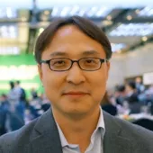
Materials Trends in Semiconductor Manufacturing
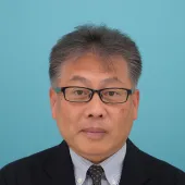
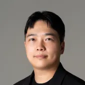
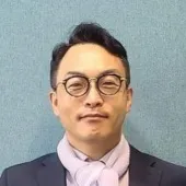
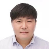
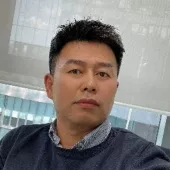
“Byunghee Kim” has been Sr. Technologist in Lam Research since 2017.
Prior to joining Lam Research, “Kim” was director position for Samsung Electronics. During his 23 years at Samsung Electronics, “Kim” spent time doing module development, including gate, contact and BEOL.
“Kim” received a bachelor’s degree in chemistry from Yonsei Univ., Seoul, Korea and a master’s degree in MSE from Seoul Nat’l Univ., Seoul, Korea.
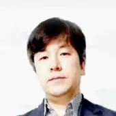
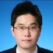
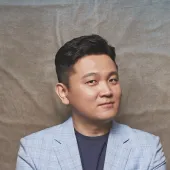
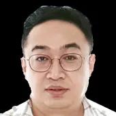
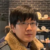
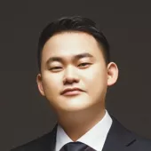
CAR Type EUV Resist Performance Improvement
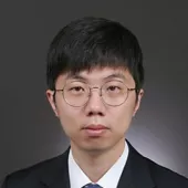
Jeongsik Kim, received a MS degree in Organic Synthetic Chemistry from Sogang University(Korean) in 2006 and then joined Dongjin Semichem. He had developed the patterning process materials such as bottom antireflective coating(BARC), spin on hardmask(SOH), photoresist materials in Semiconductor Materials Business Division since 2006. In 2013, he had joined the advanced lithography program of IMEC(Belgium) as Dongjin Semichem assignee and researched the ArF immersion patterning and defectivity for two years. Currently, he is in charge of developing EUV photoresist at Dongjin Semichem.
Lunch
Session 2: GWP
Material Innovation for low-GWP Gas Development
Sung Ho Kim is the Head of Specialty Gases Marketing, Clean & Etch platform, Merck KGaA, Darmstadt, Germany where he drives the execution of product marketing strategy to meet with industry’s dry etch and chamber clean gas technical and commercial needs, and leads product life cycle management and NPI (New product introduction) initiatives to help customers to advance its dry etch and chamber clean process performance. He is a proven business leader with more than 20 years of experience in the semiconductor materials industry, with a wide range of leadership experience in product marketing, product management, and technical/engineering expertise. He is based in Pangyo, Korea. Sung-Ho received a bachelor's degree in Chemical Engineering from Seoul National University.
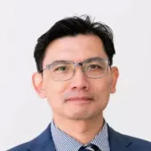
Aiming CO2 neutrality – Sustainable Solutions for IC Applications
Won-Seob Cho, Ph.D. presently serves as the Head of the BASF Electronics Materials R&D Center in Suwon, Korea. In this esteemed position, he is responsible for leading research teams dedicated to the development of advanced wet chemical solutions, such as advanced cleaning and electroplating methods. He boasts over 20 years of research and development experience, particularly in the formulation and electrochemical screening of solutions.
Prior to joining BASF a decade ago, He served as a Principal Researcher at Samsung SDI and Samsung Fine Chemicals, where he specialized in developing planarization and electroplating solutions. Notably, his research interests have recently expanded to encompass the Advanced Package field.
Won-Seob Cho holds a distinguished Ph.D. in Chemistry from the University of Texas at Austin and has also served as a postdoctoral fellow in Supramolecular Chemistry at the University of California at Los Angeles, further solidifying his scientific expertise.
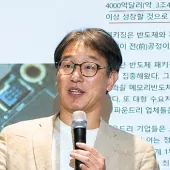
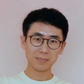
Carbon Neutral Strategy of Korean Government and Role of Material Companies
Dr. Nam, Sang Uk is conducting various studies on the ICT (semiconductor, display) industry based on economics at the KIET (Korea Institute of Industrial Research), a national research institute.
Since joining the KIET in 2018, he has participated in various studies on ICT industry policies such as Japanese export regulations, development strategy of material, parts and equipment, global value chain, and digital transformation.
In the field of carbon neutrality, he participated in major reports such as the semiconductor and display industry's carbon neutral promotion strategy and policy tasks, and the impact of RE100 on Korea's major export industries.
Session 3: Market Trends
Materials still matter. Trends in materials demand and supply.
Mark Thirsk is Managing Partner of Linx Consulting, a leading management and strategic consulting company for electronic materials.
Mark Thirsk has experience spanning many materials and processes in wafer fabrication, combined with economic and business forecasting, strategic planning, technical marketing and M&A experience. Mark has worked in materials and equipment development, marketing, applications support, and production, as well as having expertise in business incubation, strategic development, and M&A. Mark is well placed to bring clarity and insight to market analysis from both a technical and commercial perspective. Additionally, Mark has been active in SEMI since 1999, volunteering in industry advocacy, education, and recruiting.
Mark has worked in the UK, Germany, Belgium, and the USA. Mark holds an Honours B.Sc. in Metallurgy and Materials Science from Birmingham University and an MBA
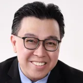
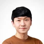
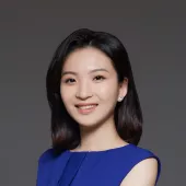
Advanced Packaging Technology & Market Trends
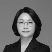
E. Jan Vardaman is president and founder of TechSearch International, Inc., which has provided market research and technology trend analysis in semiconductor packaging since 1987. She is the author of numerous publications on emerging trends in semiconductor packaging and assembly. She is a senior member of IEEE EPS and is an IEEE EPS Distinguished Lecturer. She received the IMAPS GBC Partnership award in 2012, the Daniel C. Hughes, Jr. Memorial Award in 2018, the Sidney J. Stein International Award in 2019, and she is an IMAPS Fellow. She is a member of MEPTEC, SMTA, and SEMI. Before founding TechSearch International, she served on the corporate staff of Microelectronics and Computer Technology Corporation (MCC), the electronics industry’s first pre-competitive research consortium.
Break
Session 4: Collaboration

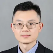
Advanced Packaging Material for Semiconductor
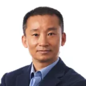
Re-visioning Material Technology for Sustainable Resource Utilization and Supply Chain
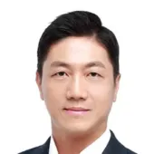
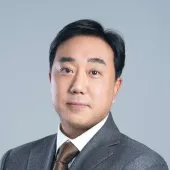
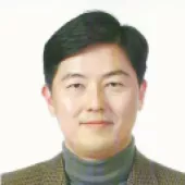
Sam-Jong Choi, Ph.D. has been working as a material expert at Samsung Electronics Semiconductor for over 30 years. He joined the company in 1991 and has been responsible as a material engineer and expert for Memory Manufacturing Technology Center in Samsung Electronics by now. He obtained a Ph.D in Electronic, Computer, and Telecommunication Engineering from Hanyang University in 2020.
In 2019, he was promoted to Group Leader for Memory Material Technology Group, where he oversaw the development of new materials and quality management for Samsung Electronics. In 2020, Samjong Choi was appointed as an Corporate VP at Samsung Electronics, where he continues to play a key role in the field of semiconductor material.
As an experienced engineer and leader, he brings a wealth of knowledge and expertise to his current role, making Samsung Electronics stay at the forefront of technological innovation in the global semiconductor material industry.
Networking Reception
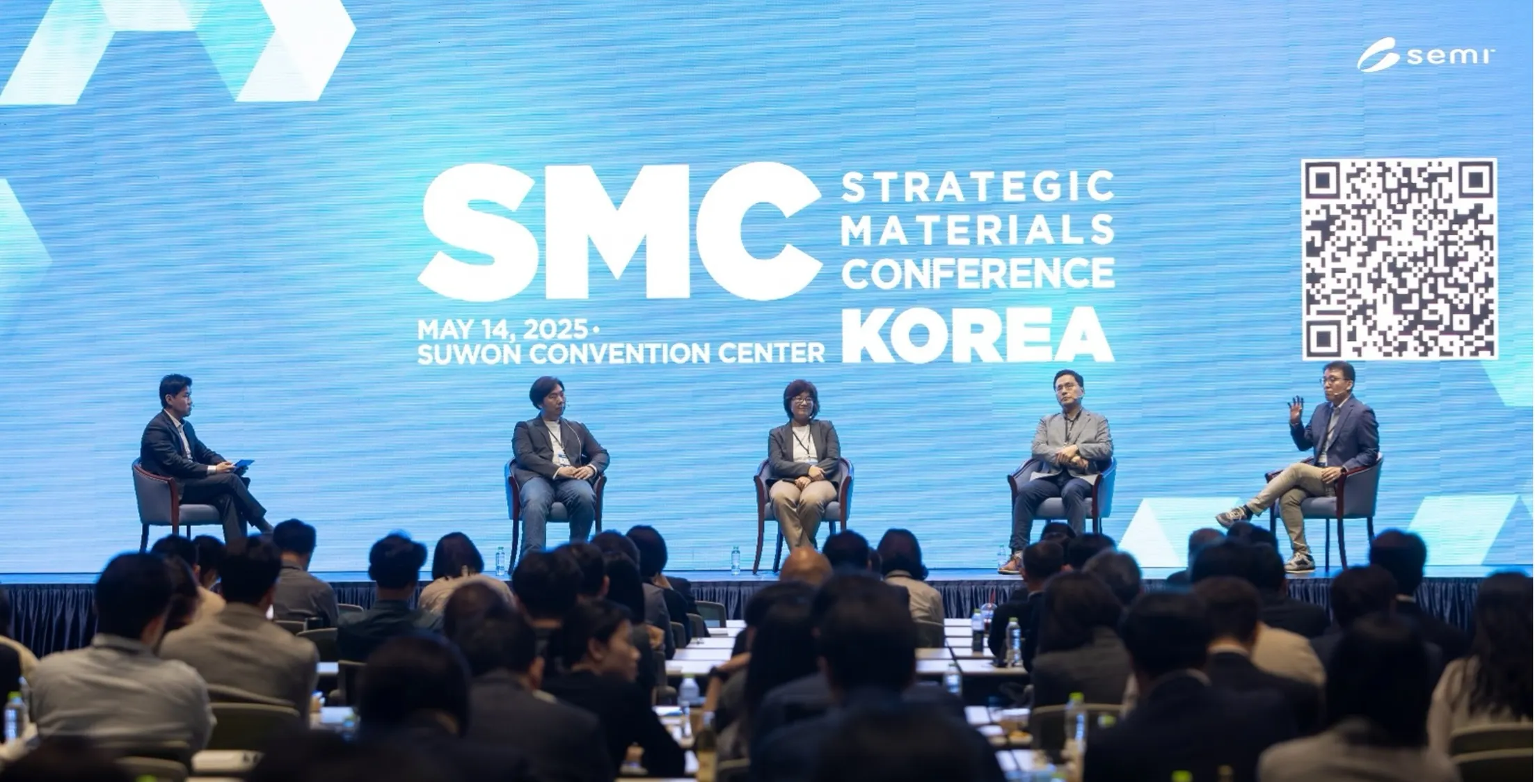
Semiconductor Materials for Sustainable Future
반도체 산업에서는 첨단 기술의 지속적인 발전만큼이나 안정적이고 효율적인 글로벌 공급망이 중요합니다. 무역갈등, 지구온난화지수(GWP)와 같은 변수 뿐만 아니라 공급망 재편 문제도 부각되고 있어 현재 반도체 생태계의 신속한 대응이 필수적인 상황입니다. 이에 SMC Korea는 반도체 업계가 함께 목소리를 내야 할 사안을 논의할 수 있는 기회를 제공하고자 합니다.
SMC Korea 2023은 글로벌 선도 기업의 참여를 통해 최신 기술과 시장에 대한 정보를 공유하는 동시에, 소재 측면에서의 GWP를 점검하는 등 다양한 관점의 발표를 준비하였습니다. 본 행사 참석을 통해 글로벌 전문가들의 인사이트를 얻어 가시기 바랍니다.